EP0124761A1 - Dispositif pour tester des échantillons contenant des circuits électriques - Google Patents
Dispositif pour tester des échantillons contenant des circuits électriques Download PDFInfo
- Publication number
- EP0124761A1 EP0124761A1 EP84103617A EP84103617A EP0124761A1 EP 0124761 A1 EP0124761 A1 EP 0124761A1 EP 84103617 A EP84103617 A EP 84103617A EP 84103617 A EP84103617 A EP 84103617A EP 0124761 A1 EP0124761 A1 EP 0124761A1
- Authority
- EP
- European Patent Office
- Prior art keywords
- circuit
- voltage
- load
- constant current
- transistor
- Prior art date
- Legal status (The legal status is an assumption and is not a legal conclusion. Google has not performed a legal analysis and makes no representation as to the accuracy of the status listed.)
- Granted
Links
- 238000012360 testing method Methods 0.000 title claims abstract description 73
- 238000011156 evaluation Methods 0.000 claims abstract description 37
- 238000005516 engineering process Methods 0.000 claims abstract description 8
- 230000000295 complement effect Effects 0.000 claims description 4
- 230000000903 blocking effect Effects 0.000 claims description 2
- 238000005070 sampling Methods 0.000 abstract description 6
- 238000010586 diagram Methods 0.000 description 2
- 230000002457 bidirectional effect Effects 0.000 description 1
- 238000011161 development Methods 0.000 description 1
- 230000018109 developmental process Effects 0.000 description 1
- RFHAOTPXVQNOHP-UHFFFAOYSA-N fluconazole Chemical compound C1=NC=NN1CC(C=1C(=CC(F)=CC=1)F)(O)CN1C=NC=N1 RFHAOTPXVQNOHP-UHFFFAOYSA-N 0.000 description 1
- 230000001960 triggered effect Effects 0.000 description 1
Images

Classifications
-
- G—PHYSICS
- G01—MEASURING; TESTING
- G01R—MEASURING ELECTRIC VARIABLES; MEASURING MAGNETIC VARIABLES
- G01R31/00—Arrangements for testing electric properties; Arrangements for locating electric faults; Arrangements for electrical testing characterised by what is being tested not provided for elsewhere
- G01R31/28—Testing of electronic circuits, e.g. by signal tracer
- G01R31/316—Testing of analog circuits
Definitions
- the invention relates to a device for testing electrical test specimens, in which an evaluation circuit is provided for evaluating test specimen signals output by the test specimen at a test specimen output and a load circuit is provided for loading the test specimen output with a definable load.
- Computer-controlled test facilities require programmable control circuits and programmable evaluation circuits for the fully automatic testing of SSI, MSL, LSI and VLSI components at every test object connection.
- the control circuit must be able to send both the corresponding signal level parameters required by the test specimen data sheet to a test specimen input and the signal level changes of the test signal to be applied to the test specimen with the required edge steepness.
- the output of the control circuit can be switched off very quickly with high resistance or switched on again.
- the device under test If the device under test is an output, it must be able to be loaded in accordance with the device under test data sheet and, in addition, the signal under test must be evaluated in terms of amplitude and time using a suitable evaluation circuit using programmable reference voltages and sampling clocks. For this reason, a programmable load circuit and a programmable evaluation circuit must be provided in the evaluation circuit.
- test device uses the test device in different circuit technologies, e.g. If ECL technology, TTL technology or MOS technology etc. are to be tested, the control circuits and evaluation circuits must cover programmable wide current and voltage ranges in order to be universally applicable. In addition, such high-frequency requirements are placed on such circuits in order to also be able to carry out dynamic tests at high test signal rates.
- the object on which the invention is based is to specify a device for testing 'test specimens containing electrical circuits, which fulfills the high RF requirements and whose space requirement on a module is nevertheless small.
- This object is achieved in a device of the type specified above in that the input of the load circuit and the input of the evaluation circuit is connected to a line leading to a connecting terminal, that the test specimen output can be connected to the connecting terminal, that at least one in the current value in the load circuit adjustable, switchable constant current source is provided, through which the device under test can be loaded in terms of current, and that at least one comparator is included in the evaluation circuit, which compares the device under test with an adjustable reference voltage at a definable time.
- each constant current source is separately adjustable in the current value and being switchable in each case. This makes it possible to load the device under test with various currents that can flow in the opposite direction.
- connection of the constant current sources with the to the lead terminal can be made via a diode bridge, in which two opposite connection points are connected to the constant current sources, the third connection point is connected to an adjustable voltage source and the diagonally opposite connection point is connected to the line to the connection terminal.
- the adjustable voltage source it can then be determined whether the load circuit operates as a load current sink or load current source, the value of the adjustable voltage source also being able to be selected such that, depending on the amplitude of the device under test, the load circuit is first used as a load current source or load current sink and then as a load current sink or load current source acts.
- the impedance and voltage level converter ensures that the input resistance of the evaluation circuit is very high-impedance and that the test-piece output is therefore not stressed by the evaluation circuit.
- the device under test signal can be adapted to the voltage values permitted for the comparators.
- FIG. 1 shows a signal generator circuit SG for generating pulse-shaped output signals or test signals, a load circuit LS and an evaluation circuit KOM.
- the output of the signal generator circuit SG, the input of the evaluation circuit KOM and the input of the load circuit LS are connected to one another at a connection point VPO.
- a line LE1 leads from the connection point VPO to a connection terminal AK, which in connection e.g. with a connector pin SF of a test specimen PR.
- Such a combination of a signal generator circuit SG, a load circuit LS and an evaluation circuit KOM is expedient if it should not be determined beforehand whether a test specimen output or a test specimen input is to be connected to the connection terminal AK.
- the output of the signal generator circuit SG must be designed in such a way that the signal generator circuit SG cannot be destroyed by the test object signals during operation in which a device under test is connected.
- the load circuit LS and the evaluation circuit KOM must then be implemented in such a way that the load circuit LS and the evaluation circuit KOM do not interfere with the operation in the operating mode in which a test specimen input is connected.
- Fig. 1 the structure of the signal generator circuit SG is shown only in principle. It can be seen that the signal generator circuit is supplied with an input signal ES, for example a TTL signal, and that control voltages UL1 and UL2 are also supplied via a first multiplexer MUX1 and control voltages UH1 and UH2 via a second multiplexer MUX2.
- the multiplexers MUX1 and MUX2 can be switched using a multiplexer signal LF.
- the control voltages UH1, UH2, UL1, UL2 can be varied, for example, between -15 volts and +15 volts.
- the amplitude voltage and the baseline voltage of the output signal AS emitted by the signal generator circuit SG can thus be set within wide ranges.
- a blocking signal TRI can be fed to the signal generator circuit, when the signal of the signal generator circuit SG is applied at high impedance.
- the evaluation circuit KOM is connected to the connection point VPO via a line LE2.
- the evaluation circuit KOM consists of an impedance and voltage level converter SK and two comparators K1 and K2.
- the converter SK is connected between the line LE2 and the one inputs of the comparators K1 and K2.
- the other inputs of the comparators K1 and K2 are each connected via multiplexers MUX3 and MUX4 to adjustable reference voltage sources which emit reference voltages UK11, UK12 and .. UK21, UK22.
- the reference voltages can be between -3Volt and +3V.
- the multiplexers MUX3 and MUX4 can in turn be switched via a Multi.plexer signal LF.
- each comparator K1, vK2 can consist of an operational amplifier OP1 or OP2 and a bistable multivibrator KS1 or KS2, into which the output value of the operational amplifiers OP1 or OP2 is adopted when the sampling clock T1 or T2 is applied.
- the converter SK With the help of the converter SK, the levels of the device under test can be converted to the input voltages permitted for the comparators K1 and K2. Furthermore, the converter SK has a high-resistance input, so that the evaluation circuit KOM hardly loads the test specimen output.
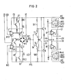
- the load circuit LS consists of a first constant current source IQ and a second constant current source IS, which are connected to a diode bridge DB.
- the constant current sources IQ, IS are located at the connection points of the diode bridge DB, from which the diodes D are poled in the same direction. These connection points are labeled VP1 and VP2.
- a third connection point VP3 of the diode bridge DB there is an adjustable control voltage source with a control voltage UC, which e.g. can be changed between + 15V and -15 volts.
- line LE2 is finally connected, which leads to terminal AK.
- the current values of the two constant current sources IQ and IS can be adjusted with the aid of guide voltages UCQ and UCS and they can each be switched, as is shown in principle in FIG. 1 by switches S1, S2.
- the switching state of the switches S1 and S2 is determined by the voltages CQ and CS.
- the load circuit LS thus loads the test specimen output in terms of current; it can either work as a load current source or load current sink.
- the positive or negative currents emitted by the load circuit LS can be changed between, ea, 50 / UA to 50 mA.
- the constant current source IQ consists of a transistor T1, which is connected to an emitter resistor RE1 is connected to the first operating potential VCC and its collector is connected to the first connection point VP1 of the diode bridge DB.
- switch S1 At the base of transistor T1 is switch S1, which can be used to block transistor T1.
- the control voltage CQ is supplied to this switch S1.
- the current value of the current source is set with the aid of an operational amplifier OP3, the input voltage of which is supplied with the guide voltage UCQ.
- the output of the operational amplifier OP3 is connected to the base of the transistor T1.
- the constant current supplied by the current source IQ into the diode bridge DB can be changed by changing the reference voltage UCQ.
- the structure of the second constant current source IS corresponds to that of the first constant current source IQ, only transistors with a complementary design are used.
- the constant current source IS contains a transistor T2 which is connected to the operating potential VEE via an emitter resistor RE2 and whose collector is connected to the connection point VP2 of the diode bridge DB.
- the second switch S2 At the base of the transistor T2 is the second switch S2, through which the transistor T2 can be blocked.
- the control voltage CS is supplied to the switch S2.
- the change in the current value, which is picked up by the constant current source IS via the diode bridge DB, is set with the aid of an operational amplifier OP4, to which the command voltage UCS is supplied and whose output is connected to the base of the transistor T2.
- the adjustable voltage source with the voltage UC is indicated at the third connection point VP3 of the diode bridge closed.
- the voltage UC determines whether the constant current source IQ or the constant current source IS loads the device under test.
- the voltage UC can be selected so that the constant current of the constant current source IQ flows through the ⁇ diodes D and the connection point VP4 to the line LE2 or it can be selected so that a current via the line LE2, the connection point VP4 and the diodes D to Constant current source IS flows.
- the voltage UC can, however, also be set such that when the level of the test object output signal changes, one constant current source first and then the other constant current source become effective.
- the load circuit LS is switched dynamically as a function of the voltage level of the device under test output signal PPS.
- the implementation of the evaluation circuit KOM in terms of circuitry also results from FIG. 2.
- the line LE2 on which the device under test signal PPS is fed to the evaluation circuit is connected to the impedance and voltage level converter SK.
- This consists of transistors T3, T4, T5, T6 and a voltage divider ST.
- the transistors T3, T4, which are complementary, are each connected to the line LE2.
- Their collectors are located on the Antoniospo - tential VEE or VCC.
- Their emitters are connected to the operating potential VCC or VEE via a series connection of two resistors each.
- the connection point of the two resistors of the series circuit SR1 is connected to the transistor T5, the connection point of the resistors of the series circuit SR2 to the transistor T6.
- the collectors of the transistors T5 and T6 are connected to the operating potential VCC and VEE.
- Their emitters are connected to the voltage divider ST via a resistor.
- the converter SK is designed in such a way that it has a high input resistance and thus the test specimen little stressed and that on the other hand it adapts the voltage level of the test object output signal to the voltage values that are permitted to operate the comparators K1 and K2.
- the output of the voltage divider ST is connected to the one input of the operational amplifier OP1 and OP2.
- the reference voltages UK11, UK12 are connected via the multiplexer MUX3 and the reference voltages UK21, UK22 via the multiplexer MUX4, as has already been shown in FIG. 1.
- the further execution of the evaluation circuit is shown in FIG. 1.
- the comparators K1 and K2 emit the output signals KA1 and KA2, the values of which determine the voltage range at the sampling time Zi, Z2 of the level of the device under test.
- the signals Z1, Z2 and the output signals KA1 and KA2 and the multiplexer signal LF can have TTL levels. The same applies to the voltages CS and CQ of the load circuit LS.
- the load circuit LS and the evaluation circuit KOM consist of relatively few components, so that it is easily possible to construct the load circuit LS and the evaluation circuit KOM on a single functional block using thick-film technology.
- the signal generator circuit SG of FIG. 1 can be implemented in a separate functional block or else on the functional block with the load circuit and the evaluation circuit KOM using thick-film technology. This results in function blocks that are very small, so that each connection element AK of the entire test facility can be assigned a separate function block without requiring a large amount of space.
Landscapes
- Engineering & Computer Science (AREA)
- General Engineering & Computer Science (AREA)
- Physics & Mathematics (AREA)
- General Physics & Mathematics (AREA)
- Tests Of Electronic Circuits (AREA)
- Testing Electric Properties And Detecting Electric Faults (AREA)
Priority Applications (1)
| Application Number | Priority Date | Filing Date | Title |
|---|---|---|---|
| AT84103617T ATE26491T1 (de) | 1983-04-08 | 1984-04-02 | Einrichtung zur pruefung von elektrische schaltkreise enthaltenden prueflingen. |
Applications Claiming Priority (2)
| Application Number | Priority Date | Filing Date | Title |
|---|---|---|---|
| DE19833312687 DE3312687A1 (de) | 1983-04-08 | 1983-04-08 | Einrichtung zur pruefung von elektrische schaltkreise enthaltenden prueflingen |
| DE3312687 | 1983-04-08 |
Publications (2)
| Publication Number | Publication Date |
|---|---|
| EP0124761A1 true EP0124761A1 (fr) | 1984-11-14 |
| EP0124761B1 EP0124761B1 (fr) | 1987-04-08 |
Family
ID=6195784
Family Applications (1)
| Application Number | Title | Priority Date | Filing Date |
|---|---|---|---|
| EP84103617A Expired EP0124761B1 (fr) | 1983-04-08 | 1984-04-02 | Dispositif pour tester des échantillons contenant des circuits électriques |
Country Status (4)
| Country | Link |
|---|---|
| US (1) | US4636716A (fr) |
| EP (1) | EP0124761B1 (fr) |
| AT (1) | ATE26491T1 (fr) |
| DE (2) | DE3312687A1 (fr) |
Cited By (1)
| Publication number | Priority date | Publication date | Assignee | Title |
|---|---|---|---|---|
| DE202009012468U1 (de) | 2009-09-12 | 2010-01-07 | Amrhein Messtechnik Gmbh | Messeinrichtung für fehlerhafte Bauteile |
Families Citing this family (9)
| Publication number | Priority date | Publication date | Assignee | Title |
|---|---|---|---|---|
| JPS6144371A (ja) * | 1984-08-06 | 1986-03-04 | Mitsubishi Electric Corp | 半導体試験装置 |
| US4745630A (en) * | 1986-06-18 | 1988-05-17 | Hughes Aircraft Company | Multi-mode counter network |
| US4761801A (en) * | 1986-06-18 | 1988-08-02 | Hughes Aircraft Company | Look ahead terminal counter |
| US5010297A (en) * | 1989-12-01 | 1991-04-23 | Analog Devices, Incorporated | Automatic test equipment with active load having high-speed inhibit mode switching |
| US5200696A (en) * | 1990-09-10 | 1993-04-06 | Ltx Corporation | Test system apparatus with Schottky diodes with programmable voltages |
| US5528137A (en) * | 1995-01-24 | 1996-06-18 | International Business Machines Corporation | Network sensitive pulse generator |
| US6323694B1 (en) | 1998-04-01 | 2001-11-27 | Ltx Corporation | Differential comparator with a programmable voltage offset for use in an automatic tester |
| US6654913B1 (en) * | 1999-02-17 | 2003-11-25 | International Business Machines Corporation | Alternate port apparatus for manufacturing test of integrated serial bus and method therefor |
| US9813050B1 (en) * | 2016-04-13 | 2017-11-07 | Analog Devices, Inc. | Comparator circuit with input attenuator |
Citations (4)
| Publication number | Priority date | Publication date | Assignee | Title |
|---|---|---|---|---|
| DE2429836A1 (de) * | 1973-06-25 | 1975-01-23 | Ibm | Verfahren zur bestimmung des stabilitaetsverhaltens von halbleiterschaltungen |
| GB1416786A (en) * | 1972-03-27 | 1975-12-10 | Ibm | Method of testing an integrated circuit block |
| DE3106727A1 (de) * | 1980-02-27 | 1982-02-11 | Racal Automation Ltd., Bracknell, Berkshire | "verfahren und vorrichtung zum automatischen pruefen elektrischer und elektronischer schaltkreise" |
| DE3218814A1 (de) * | 1981-05-28 | 1982-12-16 | Zehntel, Inc., 94598 Walnut Creek, Calif. | Digitaler in-schaltkreis-tester |
Family Cites Families (2)
| Publication number | Priority date | Publication date | Assignee | Title |
|---|---|---|---|---|
| JPS5873881A (ja) * | 1981-10-29 | 1983-05-04 | Advantest Corp | Icテスタ |
| US4495462A (en) * | 1983-03-03 | 1985-01-22 | Raytheon Company | Current source test circuitry |
-
1983
- 1983-04-08 DE DE19833312687 patent/DE3312687A1/de not_active Withdrawn
-
1984
- 1984-04-02 DE DE8484103617T patent/DE3463091D1/de not_active Expired
- 1984-04-02 AT AT84103617T patent/ATE26491T1/de not_active IP Right Cessation
- 1984-04-02 EP EP84103617A patent/EP0124761B1/fr not_active Expired
- 1984-04-06 US US06/597,720 patent/US4636716A/en not_active Expired - Fee Related
Patent Citations (4)
| Publication number | Priority date | Publication date | Assignee | Title |
|---|---|---|---|---|
| GB1416786A (en) * | 1972-03-27 | 1975-12-10 | Ibm | Method of testing an integrated circuit block |
| DE2429836A1 (de) * | 1973-06-25 | 1975-01-23 | Ibm | Verfahren zur bestimmung des stabilitaetsverhaltens von halbleiterschaltungen |
| DE3106727A1 (de) * | 1980-02-27 | 1982-02-11 | Racal Automation Ltd., Bracknell, Berkshire | "verfahren und vorrichtung zum automatischen pruefen elektrischer und elektronischer schaltkreise" |
| DE3218814A1 (de) * | 1981-05-28 | 1982-12-16 | Zehntel, Inc., 94598 Walnut Creek, Calif. | Digitaler in-schaltkreis-tester |
Cited By (1)
| Publication number | Priority date | Publication date | Assignee | Title |
|---|---|---|---|---|
| DE202009012468U1 (de) | 2009-09-12 | 2010-01-07 | Amrhein Messtechnik Gmbh | Messeinrichtung für fehlerhafte Bauteile |
Also Published As
| Publication number | Publication date |
|---|---|
| US4636716A (en) | 1987-01-13 |
| ATE26491T1 (de) | 1987-04-15 |
| DE3312687A1 (de) | 1984-10-18 |
| DE3463091D1 (en) | 1987-05-14 |
| EP0124761B1 (fr) | 1987-04-08 |
Similar Documents
| Publication | Publication Date | Title |
|---|---|---|
| DE68912982T2 (de) | Verfahren und Anordnung zum Testen mehrfacher Speiseverbindungen einer integrierten Schaltung auf einer Printplatte. | |
| DE60308870T2 (de) | Kompensation von testsignalverschlechterung aufgrund einer fehlfunktion des zu testenden bauelements | |
| DE69004830T2 (de) | Anordnung zum Ermitteln eines Ruhestroms einer integrierten monolithischen digitalen Schaltung, integrierte monolithische digitale Schaltung mit einer derartigen Anordnung und Prüfgerät mit einer derartigen Anordnung. | |
| DE69125459T2 (de) | Aktiver programmierbarer Leitungsabschluss für automatische Testempfänger | |
| DE3884049T2 (de) | System zur Übertragungskontrolle eines integrierten Schaltkreises. | |
| DE69733789T2 (de) | Hochauflösendes Stromversorgungsprüfsystem | |
| DE60100109T2 (de) | Umschaltbare Testschaltung für asymmetrischen und differentiellen Abschluss | |
| DE69811950T2 (de) | Elektronische überwachungsschaltung für elektrische spannung | |
| EP0124761B1 (fr) | Dispositif pour tester des échantillons contenant des circuits électriques | |
| EP0074417B1 (fr) | Procédé et circuit pour tester un circuit intégré avec un circuit excitateur tri-stable qui contrôle celui-ci dans l'état d'impédance de sortie élevé | |
| WO2005052612A2 (fr) | Circuit d'entree et de sortie d'un circuit de commutation integre, procede pour tester un circuit de commutation integre et circuit de commutation integre dote d'un circuit d'entree et de sortie de ce type | |
| DE69406942T2 (de) | Abtastprüfungsschaltung mit schnellem übertragungsgateschalter | |
| EP0093996A1 (fr) | Circuit pour la conversion de niveau | |
| EP1217630A2 (fr) | Procédé de test d'un circuit integré | |
| DE69021036T2 (de) | Test-Anordnungssystem für integrierte Schaltungen unter Verwendung von lateralen Transistoren. | |
| DE69426720T2 (de) | Halbleiterschaltungsanordnung mit einer Kombination von CMOS- und bipolaren Schaltungen | |
| DE69128116T2 (de) | Flash-A/D-Wandler mit Prüfschaltung | |
| DE10393795T5 (de) | Impulserzeugungsschaltung und Abtastschaltung | |
| DE60021314T2 (de) | Anordnung für spitzenstrom prüfung einer digitalen elektronischen cmos schaltung | |
| DE10341836B4 (de) | Testvorrichtung zum Testen von elektrischen Schaltungen sowie Verfahren zum parallelen Testen von elektrischen Schaltungen | |
| DE3009014C2 (fr) | ||
| DE102021124919B4 (de) | Partitioniertes force-sense-system für eine prüfeinrichtung | |
| DE10243603B4 (de) | Verfahren zur Verwendung beim Trimmen, Halbleiter-Bauelement-Test-Gerät zum Durchführen des Verfahrens und Halbleiter-Bauelement-Test-System | |
| DE3880522T2 (de) | Triggeranordnung. | |
| EP0093899B1 (fr) | Circuit pour l'adaptation d'un dispositif d'essai à un objet à l'essai |
Legal Events
| Date | Code | Title | Description |
|---|---|---|---|
| PUAI | Public reference made under article 153(3) epc to a published international application that has entered the european phase |
Free format text: ORIGINAL CODE: 0009012 |
|
| AK | Designated contracting states |
Designated state(s): AT CH DE FR GB IT LI |
|
| 17P | Request for examination filed |
Effective date: 19841221 |
|
| GRAA | (expected) grant |
Free format text: ORIGINAL CODE: 0009210 |
|
| AK | Designated contracting states |
Kind code of ref document: B1 Designated state(s): AT CH DE FR GB IT LI |
|
| REF | Corresponds to: |
Ref document number: 26491 Country of ref document: AT Date of ref document: 19870415 Kind code of ref document: T |
|
| REF | Corresponds to: |
Ref document number: 3463091 Country of ref document: DE Date of ref document: 19870514 |
|
| ET | Fr: translation filed | ||
| ITF | It: translation for a ep patent filed | ||
| PLBE | No opposition filed within time limit |
Free format text: ORIGINAL CODE: 0009261 |
|
| STAA | Information on the status of an ep patent application or granted ep patent |
Free format text: STATUS: NO OPPOSITION FILED WITHIN TIME LIMIT |
|
| 26N | No opposition filed | ||
| PGFP | Annual fee paid to national office [announced via postgrant information from national office to epo] |
Ref country code: GB Payment date: 19910318 Year of fee payment: 8 |
|
| PGFP | Annual fee paid to national office [announced via postgrant information from national office to epo] |
Ref country code: AT Payment date: 19910327 Year of fee payment: 8 |
|
| PGFP | Annual fee paid to national office [announced via postgrant information from national office to epo] |
Ref country code: FR Payment date: 19910423 Year of fee payment: 8 |
|
| ITTA | It: last paid annual fee | ||
| PGFP | Annual fee paid to national office [announced via postgrant information from national office to epo] |
Ref country code: DE Payment date: 19910626 Year of fee payment: 8 |
|
| PGFP | Annual fee paid to national office [announced via postgrant information from national office to epo] |
Ref country code: CH Payment date: 19910724 Year of fee payment: 8 |
|
| PG25 | Lapsed in a contracting state [announced via postgrant information from national office to epo] |
Ref country code: GB Effective date: 19920402 Ref country code: AT Effective date: 19920402 |
|
| PG25 | Lapsed in a contracting state [announced via postgrant information from national office to epo] |
Ref country code: LI Effective date: 19920430 Ref country code: CH Effective date: 19920430 |
|
| GBPC | Gb: european patent ceased through non-payment of renewal fee | ||
| PG25 | Lapsed in a contracting state [announced via postgrant information from national office to epo] |
Ref country code: FR Effective date: 19921230 |
|
| REG | Reference to a national code |
Ref country code: CH Ref legal event code: PL |
|
| PG25 | Lapsed in a contracting state [announced via postgrant information from national office to epo] |
Ref country code: DE Effective date: 19930101 |
|
| REG | Reference to a national code |
Ref country code: FR Ref legal event code: ST |