EP0124942A1 - Integrierte Speicheranordnung in Seriell-Parallel-Seriellorganisation - Google Patents
Integrierte Speicheranordnung in Seriell-Parallel-Seriellorganisation Download PDFInfo
- Publication number
- EP0124942A1 EP0124942A1 EP84200629A EP84200629A EP0124942A1 EP 0124942 A1 EP0124942 A1 EP 0124942A1 EP 84200629 A EP84200629 A EP 84200629A EP 84200629 A EP84200629 A EP 84200629A EP 0124942 A1 EP0124942 A1 EP 0124942A1
- Authority
- EP
- European Patent Office
- Prior art keywords
- clock signal
- circuit
- memory circuit
- input
- write
- Prior art date
- Legal status (The legal status is an assumption and is not a legal conclusion. Google has not performed a legal analysis and makes no representation as to the accuracy of the status listed.)
- Granted
Links
- 238000003708 edge detection Methods 0.000 claims description 4
- 230000001934 delay Effects 0.000 description 3
- 238000010276 construction Methods 0.000 description 1
- 238000010586 diagram Methods 0.000 description 1
- 230000006870 function Effects 0.000 description 1
Images
Classifications
-
- G—PHYSICS
- G11—INFORMATION STORAGE
- G11C—STATIC STORES
- G11C19/00—Digital stores in which the information is moved stepwise, e.g. shift registers
- G11C19/28—Digital stores in which the information is moved stepwise, e.g. shift registers using semiconductor elements
- G11C19/282—Digital stores in which the information is moved stepwise, e.g. shift registers using semiconductor elements with charge storage in a depletion layer, i.e. charge coupled devices [CCD]
- G11C19/285—Peripheral circuits, e.g. for writing into the first stage; for reading-out of the last stage
-
- G—PHYSICS
- G11—INFORMATION STORAGE
- G11C—STATIC STORES
- G11C5/00—Details of stores covered by group G11C11/00
- G11C5/06—Arrangements for interconnecting storage elements electrically, e.g. by wiring
- G11C5/066—Means for reducing external access-lines for a semiconductor memory clip, e.g. by multiplexing at least address and data signals
-
- G—PHYSICS
- G11—INFORMATION STORAGE
- G11C—STATIC STORES
- G11C7/00—Arrangements for writing information into, or reading information out from, a digital store
- G11C7/22—Read-write [R-W] timing or clocking circuits; Read-write [R-W] control signal generators or management
-
- G—PHYSICS
- G11—INFORMATION STORAGE
- G11C—STATIC STORES
- G11C8/00—Arrangements for selecting an address in a digital store
- G11C8/18—Address timing or clocking circuits; Address control signal generation or management, e.g. for row address strobe [RAS] or column address strobe [CAS] signals
Definitions
- the invention relates to an integrated memory circuit of a series-parallel-series type comprising a write register, a transfer circuit having a plurality of transfer registers which are operative in parallel in the operating state, and a read register, the write register being controllable by a write clock signal of a write clock signal frequency, the transfer circuit by a transfer clock signal of a transfer clock signal frequency and the read register by a read clock signal of a read clock signal frequency.
- the invention has for its .object to reduce the number of connecting pins of such a memory circuit while preserving substantially all the fields of application.
- an integrated memory circuit of the type set forth in the opening paragraph is characterized in that the memory circuit comprises a clock signal processing circuit having a first input for a signal of the write or read clock signal frequency coupled to a first clock signal input of the memory circuit and a second input for a signal of the transfer clock signal frequency coupled toa second clock signal input of the memory circuit, a first output for the write clock signal, a second output for the transfer clock signal and a third output for the read clock signal, the clock signal processing circuit being arranged for deriving only from the signals at the first and second inputs the write, transfer and read clock signals.
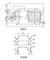
- FIG. 1 a video signal which is illustrated in Figure 2 by means of a waveform 201 is applied to an input 1 of an integrated memory circuit 3.
- the input 1 of the memory circuit 3 is connected to an input 5 of a write register 7.
- the write register 7 is connected via a transfer circuit 9 having a number of parallel operating transfer registers 11 to 11 n to a read register 13 an output 15 of which is connected to an output 17 of the memory circuit 3.
- a waveform 217 illustrates the video signal at the output 17 of the memory circuit 3 if this memory circuit is used as a field delay circuit having a time delay of, for example, a field period minus half a line period.
- the write register 7 has a write clock signal input 19, which receives a write clock signal from a first output 21 of a clock signal processing circuit 23.
- the transfer circuit 9 has a transfer clock signal input 25 which from a second output 27 of the clock signal processing circuit receives a clock signal which is illustrated in Figure 2 by means of a waveform 227.
- a read clock signal is obtained which is applied to a read clock signal input 31 of the read register 13.
- the clock signal processing circuit 23 has a first input 33, connected to a pin 35, which serves as a first clock signal input of the memory circuit 3 and a second input 37, connected to a pin 39, which serves as a second clock signal input of the memory circuit 3.
- a first clock signal which has a high write or read clock frequency and is not shown in Figure 2 is applied to the first input 33 of the clock signal processing circuit 23, and a second clock signal which has a low transfer clock frequency and is illustrated in Figure 2 by means of a waveform 237 is applied to the second input 37 of the clock signal processing circuit 23.
- the inputs 3 and 37 are connected to the inputs of an AND-gate 41 whose output is connected to the outputs 21 and 29 of the clock signal processing circuit. This causes the first clock signal at these outputs 21 and 29 to occur only during the periods, shown in Figure 2 as ... -t 1 , t 2 - t 4 , t 5 ...., in which the second clock signal is high.
- the inputs 33 and 37 of the clock signal processing circuit 23 are further connected to inputs 43 and 45, respectively, of an edge detection circuit 47.
- the input 43 of this edge detection circuit 47 is connected to a clock signal input of a D-flip-flop 49 and the input 45 to an input of this flip-flop and to an inverting input of an AND-gate 51, whose other input is connected to an output of the flip-flop 49.
- the output of the AND-gate 51 is connected to the output 27 of the clock signal processing circuit 23.
- the D-flip-flop 49 delays the second clock signal applied to the input 45 by a time corresponding to the period of the first clock signal at the input 43, which causes the trailing edges of the second clock signal 237, which edges occur at the instants t 1 , t 4 , ...., to produce a pulse at the output 27 as shown in the waveform 227.
- These pulses 227 attend to the transfer from the write register 7 to the read register 13 and occur at the end of the writing periods. If it is ensured that these pulses coincide with the end of the line trace period then at each of these moments a portion of the video signal which occurs in the periods ...-t 1 , t 3 -t 4 , t 6 Vietnamese is stored in the write register 7, these periods having a duration depending on the length of the write register 7, which length is here assumed to be equal to the line trace period T .
- Reading the read register 13 always starts at the instants ...., t 2' t 5 , .... as a result of which the delay of the memory circuit becomes equal to the field period minus half a line period minus x, where x is the time difference between t 2 and t 3 , t 5 and t 6 , ....
- the time delay of the memory circuit By shifting the leading edge in the second clock signal 237 it is not possible to make for example, the time delay of the memory circuit, such that together with delays in signal processing circuits outside the memory circuit 3 these delays become equal to a field period minus half a line period as is required for many circuits.
- the write clock signal input 19 of the write register 7 can if so desired be connected to the input 33 of the clock signal processing circuit 23 instead of to the output of the AND-gate 41 as shown by means of a dotted line in Figure 1.
- edge detection circuit 47 may alternatively be used for the edge detection circuit 47 and the AND-gate 41.
- the transfer clock signal 227 is derived from the trailing edges of the second clock signal 237 the periodically temporarily accelerated transfer remains possible in circuits for which the memory length of the memory circuit 3 is too long. This is then effected by increasing periodically and temporarily the frequency of the second clock signal. The information written-in in this period is then not suitable for use, which is not important. For the sake of clarity, only one phase of the clock signals is shown; when the memory circuit requires multi-phase clock signals these signals can, for example, be generated in known manners.
- the memory circuit is a circuit for processing binary signal combinations then additional, parallel- operating combinations of write, transfer and read registers can be included in the integrated circuit, each register processing a bit of these signal combinations.
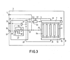
- a charge destruct circuit 52 is preferably included at the end of the write register 7, as shown in Figure 3, and between the input 1 of the memory circuit 3 and the input 5 of the write register 7 a shift register 53 is arranged which is formed by some flip-flops which are each set by pulses applied to a setting input 55 and originating from the output 27 of the clock signal processing circuit 23 and to which the write clock signal originating from the output 21 of the clock signal processing circuit 23 is applied via a clock signal input 57 of the register 53:
- the reliability of the operation of the clock signal processing circuit 23 can, if so desired, be still further improved by providing a D-flip-flop between the second clock signal input 39 of the memory circuit 3 and the input 37 of the clock signal processing circuit 23. This D-flip-flop must then receive its clock signal from the first clock signal input 35 of the memory circuit
Landscapes
- Engineering & Computer Science (AREA)
- Microelectronics & Electronic Packaging (AREA)
- Dram (AREA)
- Pulse Circuits (AREA)
- Processing Of Color Television Signals (AREA)
Applications Claiming Priority (2)
| Application Number | Priority Date | Filing Date | Title |
|---|---|---|---|
| NL8301603A NL8301603A (nl) | 1983-05-06 | 1983-05-06 | Geintegreerde geheugenschakeling van een serie-parallel-serie type. |
| NL8301603 | 1983-05-06 |
Publications (2)
| Publication Number | Publication Date |
|---|---|
| EP0124942A1 true EP0124942A1 (de) | 1984-11-14 |
| EP0124942B1 EP0124942B1 (de) | 1987-10-28 |
Family
ID=19841814
Family Applications (1)
| Application Number | Title | Priority Date | Filing Date |
|---|---|---|---|
| EP84200629A Expired EP0124942B1 (de) | 1983-05-06 | 1984-05-03 | Integrierte Speicheranordnung in Seriell-Parallel-Seriellorganisation |
Country Status (6)
| Country | Link |
|---|---|
| US (1) | US4599710A (de) |
| EP (1) | EP0124942B1 (de) |
| JP (1) | JPS59229779A (de) |
| AU (1) | AU564558B2 (de) |
| DE (1) | DE3467061D1 (de) |
| NL (1) | NL8301603A (de) |
Cited By (2)
| Publication number | Priority date | Publication date | Assignee | Title |
|---|---|---|---|---|
| FR2645384A1 (fr) * | 1989-04-04 | 1990-10-05 | Europ Rech Electr Lab | Dispositif et procede de generation de signaux de controle |
| US5249229A (en) * | 1989-04-04 | 1993-09-28 | Laboratoire Europeen De Recherches Electroniques Avancees Societe En Nom Collectif | Device and method for generating control signals |
Families Citing this family (6)
| Publication number | Priority date | Publication date | Assignee | Title |
|---|---|---|---|---|
| US4745577A (en) * | 1984-11-20 | 1988-05-17 | Fujitsu Limited | Semiconductor memory device with shift registers for high speed reading and writing |
| US4884198A (en) * | 1986-12-18 | 1989-11-28 | Sun Microsystems, Inc. | Single cycle processor/cache interface |
| DE3832328A1 (de) * | 1988-09-23 | 1990-03-29 | Broadcast Television Syst | Speicheranordnung fuer digitale signale |
| JP3333265B2 (ja) * | 1993-04-28 | 2002-10-15 | セイコーインスツルメンツ株式会社 | 半導体集積回路 |
| US5565816A (en) * | 1995-08-18 | 1996-10-15 | International Business Machines Corporation | Clock distribution network |
| FI109263B (fi) * | 2000-10-26 | 2002-06-14 | Teknoware Oy | Menetelmä ja järjestelmä toimintatilatiedon keräämiseksi |
Citations (1)
| Publication number | Priority date | Publication date | Assignee | Title |
|---|---|---|---|---|
| US4117546A (en) * | 1977-12-30 | 1978-09-26 | International Business Machines Corporation | Interlaced ccd memory |
Family Cites Families (2)
| Publication number | Priority date | Publication date | Assignee | Title |
|---|---|---|---|---|
| US3763480A (en) * | 1971-10-12 | 1973-10-02 | Rca Corp | Digital and analog data handling devices |
| JPS5680887A (en) * | 1979-12-03 | 1981-07-02 | Hitachi Ltd | Electric charge transfer memory device |
-
1983
- 1983-05-06 NL NL8301603A patent/NL8301603A/nl not_active Application Discontinuation
-
1984
- 1984-05-01 US US06/605,958 patent/US4599710A/en not_active Expired - Fee Related
- 1984-05-02 JP JP59087922A patent/JPS59229779A/ja active Pending
- 1984-05-03 DE DE8484200629T patent/DE3467061D1/de not_active Expired
- 1984-05-03 EP EP84200629A patent/EP0124942B1/de not_active Expired
- 1984-05-04 AU AU27684/84A patent/AU564558B2/en not_active Ceased
Patent Citations (1)
| Publication number | Priority date | Publication date | Assignee | Title |
|---|---|---|---|---|
| US4117546A (en) * | 1977-12-30 | 1978-09-26 | International Business Machines Corporation | Interlaced ccd memory |
Non-Patent Citations (1)
| Title |
|---|
| ELECTRONIC DESIGN, vol. 26, no. 17, 16th August 1978, pages 88-94, Rochelle Park, USA; D. SITRICK: "Single-chip CCD memory really delivers: Besides 64-kbit density, the TMS3064 offers high speed and economical bulk storage-and consumes very little power" * |
Cited By (4)
| Publication number | Priority date | Publication date | Assignee | Title |
|---|---|---|---|---|
| FR2645384A1 (fr) * | 1989-04-04 | 1990-10-05 | Europ Rech Electr Lab | Dispositif et procede de generation de signaux de controle |
| EP0391784A1 (de) * | 1989-04-04 | 1990-10-10 | Laboratoire Europeen De Recherches Electroniques Avancees | Einrichtung und Verfahren zur Erzeugung von Steuersignalen |
| WO1990012471A1 (fr) * | 1989-04-04 | 1990-10-18 | Laboratoire Europeen De Recherches Electroniques Avancees | Dispositif et procede de generation de signaux de controle |
| US5249229A (en) * | 1989-04-04 | 1993-09-28 | Laboratoire Europeen De Recherches Electroniques Avancees Societe En Nom Collectif | Device and method for generating control signals |
Also Published As
| Publication number | Publication date |
|---|---|
| US4599710A (en) | 1986-07-08 |
| AU2768484A (en) | 1984-11-08 |
| AU564558B2 (en) | 1987-08-13 |
| JPS59229779A (ja) | 1984-12-24 |
| DE3467061D1 (en) | 1987-12-03 |
| NL8301603A (nl) | 1984-12-03 |
| EP0124942B1 (de) | 1987-10-28 |
Similar Documents
| Publication | Publication Date | Title |
|---|---|---|
| EP3907886B1 (de) | Vorrichtung zur datensynchronisation in systemen mit mehreren takt- und rücksetzdomänen | |
| US5459736A (en) | Scan path circuit for testing multi-phase clocks from sequential circuits | |
| US4945516A (en) | Write control circuit for a high-speed memory device | |
| US4949249A (en) | Clock skew avoidance technique for pipeline processors | |
| US4599710A (en) | Integrated memory circuit of a series-parallel-series type | |
| CN212622809U (zh) | 检测电路 | |
| US6075833A (en) | Method and apparatus for counting signal transitions | |
| US5132993A (en) | Shift register circuit | |
| JPS5923647A (ja) | 直列デ−タ信号の変換方法および変換回路 | |
| CN114076849B (zh) | 检测电路和检测方法 | |
| US6930522B2 (en) | Method and apparatus to delay signal latching | |
| EP0511423A1 (de) | Elektrischer Schaltkreis zum Generieren von Impulsreihen | |
| US6999542B1 (en) | Data ready indicator between different clock domains | |
| US4777448A (en) | Frequency multiplying circuit | |
| US4270116A (en) | High speed data logical comparison device | |
| US11402431B2 (en) | Detection circuit and detection method | |
| US3671960A (en) | Four phase encoder system for three frequency modulation | |
| US4741005A (en) | Counter circuit having flip-flops for synchronizing carry signals between stages | |
| US3851154A (en) | Output preview arrangement for shift registers | |
| US5065041A (en) | Timing generator module | |
| US4901315A (en) | Integrated data and timing circuitry for automatic circuit tester | |
| KR20010006850A (ko) | 스큐 포인터 발생 회로 및 방법 | |
| US5942927A (en) | Clock signal generator for a logic analyzer controlled to lock both edges to a reference clock signal | |
| RU2806240C1 (ru) | Схема обнаружения и способ обнаружения | |
| JP2783495B2 (ja) | クロック乗せ換え回路 |
Legal Events
| Date | Code | Title | Description |
|---|---|---|---|
| PUAI | Public reference made under article 153(3) epc to a published international application that has entered the european phase |
Free format text: ORIGINAL CODE: 0009012 |
|
| AK | Designated contracting states |
Designated state(s): DE FR GB IT |
|
| 17P | Request for examination filed |
Effective date: 19841219 |
|
| 17Q | First examination report despatched |
Effective date: 19860612 |
|
| GRAA | (expected) grant |
Free format text: ORIGINAL CODE: 0009210 |
|
| AK | Designated contracting states |
Kind code of ref document: B1 Designated state(s): DE FR GB IT |
|
| REF | Corresponds to: |
Ref document number: 3467061 Country of ref document: DE Date of ref document: 19871203 |
|
| ITF | It: translation for a ep patent filed | ||
| ET | Fr: translation filed | ||
| PLBE | No opposition filed within time limit |
Free format text: ORIGINAL CODE: 0009261 |
|
| STAA | Information on the status of an ep patent application or granted ep patent |
Free format text: STATUS: NO OPPOSITION FILED WITHIN TIME LIMIT |
|
| 26N | No opposition filed | ||
| PGFP | Annual fee paid to national office [announced via postgrant information from national office to epo] |
Ref country code: GB Payment date: 19900430 Year of fee payment: 7 |
|
| PGFP | Annual fee paid to national office [announced via postgrant information from national office to epo] |
Ref country code: FR Payment date: 19900522 Year of fee payment: 7 |
|
| PGFP | Annual fee paid to national office [announced via postgrant information from national office to epo] |
Ref country code: DE Payment date: 19900725 Year of fee payment: 7 |
|
| PG25 | Lapsed in a contracting state [announced via postgrant information from national office to epo] |
Ref country code: GB Effective date: 19910503 |
|
| GBPC | Gb: european patent ceased through non-payment of renewal fee | ||
| PG25 | Lapsed in a contracting state [announced via postgrant information from national office to epo] |
Ref country code: FR Effective date: 19920131 |
|
| PG25 | Lapsed in a contracting state [announced via postgrant information from national office to epo] |
Ref country code: DE Effective date: 19920303 |
|
| REG | Reference to a national code |
Ref country code: FR Ref legal event code: ST |