EP0124954A2 - Halbleiteranordnungen mit Elementen aus Metallsiliziden - Google Patents
Halbleiteranordnungen mit Elementen aus Metallsiliziden Download PDFInfo
- Publication number
- EP0124954A2 EP0124954A2 EP84300674A EP84300674A EP0124954A2 EP 0124954 A2 EP0124954 A2 EP 0124954A2 EP 84300674 A EP84300674 A EP 84300674A EP 84300674 A EP84300674 A EP 84300674A EP 0124954 A2 EP0124954 A2 EP 0124954A2
- Authority
- EP
- European Patent Office
- Prior art keywords
- layer
- silicide
- metallic silicide
- gate
- silicon
- Prior art date
- Legal status (The legal status is an assumption and is not a legal conclusion. Google has not performed a legal analysis and makes no representation as to the accuracy of the status listed.)
- Withdrawn
Links
Images

Classifications
-
- H—ELECTRICITY
- H10—SEMICONDUCTOR DEVICES; ELECTRIC SOLID-STATE DEVICES NOT OTHERWISE PROVIDED FOR
- H10D—INORGANIC ELECTRIC SEMICONDUCTOR DEVICES
- H10D30/00—Field-effect transistors [FET]
- H10D30/01—Manufacture or treatment
- H10D30/021—Manufacture or treatment of FETs having insulated gates [IGFET]
- H10D30/0223—Manufacture or treatment of FETs having insulated gates [IGFET] having source and drain regions or source and drain extensions self-aligned to sides of the gate
-
- H—ELECTRICITY
- H10—SEMICONDUCTOR DEVICES; ELECTRIC SOLID-STATE DEVICES NOT OTHERWISE PROVIDED FOR
- H10D—INORGANIC ELECTRIC SEMICONDUCTOR DEVICES
- H10D64/00—Electrodes of devices having potential barriers
- H10D64/01—Manufacture or treatment
- H10D64/013—Manufacture or treatment of electrodes having a conductor capacitively coupled to a semiconductor by an insulator
- H10D64/01302—Manufacture or treatment of electrodes having a conductor capacitively coupled to a semiconductor by an insulator the insulator being formed after the semiconductor body, the semiconductor being silicon
- H10D64/01304—Manufacture or treatment of electrodes having a conductor capacitively coupled to a semiconductor by an insulator the insulator being formed after the semiconductor body, the semiconductor being silicon characterised by the conductor
- H10D64/01318—Manufacture or treatment of electrodes having a conductor capacitively coupled to a semiconductor by an insulator the insulator being formed after the semiconductor body, the semiconductor being silicon characterised by the conductor the conductor comprising a layer of alloy material, compound material or organic material contacting the insulator, e.g. TiN
- H10D64/0132—Manufacture or treatment of electrodes having a conductor capacitively coupled to a semiconductor by an insulator the insulator being formed after the semiconductor body, the semiconductor being silicon characterised by the conductor the conductor comprising a layer of alloy material, compound material or organic material contacting the insulator, e.g. TiN the conductor being a metallic silicide
-
- H—ELECTRICITY
- H10—SEMICONDUCTOR DEVICES; ELECTRIC SOLID-STATE DEVICES NOT OTHERWISE PROVIDED FOR
- H10W—GENERIC PACKAGES, INTERCONNECTIONS, CONNECTORS OR OTHER CONSTRUCTIONAL DETAILS OF DEVICES COVERED BY CLASS H10
- H10W20/00—Interconnections in chips, wafers or substrates
- H10W20/01—Manufacture or treatment
- H10W20/031—Manufacture or treatment of conductive parts of the interconnections
- H10W20/064—Manufacture or treatment of conductive parts of the interconnections by modifying the conductivity of conductive parts, e.g. by alloying
- H10W20/066—Manufacture or treatment of conductive parts of the interconnections by modifying the conductivity of conductive parts, e.g. by alloying by forming silicides of refractory metals
Definitions
- This invention relates to semiconductor devices and the manufacture thereof and, in particular, to semiconductor processing employing silicides.
- Polysilicon has conventionally been employed for gates and interconnections in integrated circuits. However, for small geometry, high speed integrated circuits it is desirable to use alternative materials with lower resistivity, such as silicide materials.
- the resistivity of polysilicon is high (1000% ⁇ cm) and roughly fifty times larger than some silicides, for example titanium disilicide has a resistivity of 20 ⁇ cm, and thus interconnections of polysilicon are extremely resistive in fine-line circuits.
- the propagational delay of electrical signals in such interconnect lines is a function of the product of the lumped capacitance and resistance of the interconnect line. As devices sizes are scaled down to achieve higher packing densities and speeds, this delay becomes dominated by the resistive component and thus new materials must be used.
- Silicides comprise such alternative materials which can be entirely compatible with the other components of the manufacturing process. Provided that the introduction of the material does not significantly perturb the existing process, the advantage of the new material can also be exploited in present day technologies.
- a process has been developed whereby the silicide is formed by interdiffusing a layer of metal (tungsten, molybdenum, titanium, tantalum, etc.) with a sheet of doped polysilicon used to form the conventional gate and interconnects. This heterogeneous layer is then etched to form the gate and interconnects of the device.
- metal tungsten, molybdenum, titanium, tantalum, etc.
- This heterogeneous layer is then etched to form the gate and interconnects of the device.
- the silicide overlying the doped polysilicon etches at different rates from the polysilicon, some undesirable undercutting at the gate occurs.
- a method of manufacturing semiconductor devices including the steps of depositing a layer of a silicon rich homogeneous metallic silicide on an oxidised surface of a silicon substrate and patterning the layer to define at least one metallic silicide element on the oxidised surface.
- Figs. la to c The known process shown in Figs. la to c comprises the following steps.
- an oxide layer 2 which is thin in the area where source, drain and gate regions of the device are to be formed, is provided by conventional means.
- a layer of doped polycrystalline silicon (polysilicon) 3 is provided over the oxide 2 (Fig.la).
- a metal layer 4 (Fig. lb) of, for example, tungsten, molybdenum, titanium or tantalum, is deposited on the polysilicon layer 3.
- a metallic silicide layer (Fig. lc) is formed by interdiffusing layers 3 and 4.
- the structure is then etched to form the gate 6 of the device and interconnects (not shown) and, because the silicide 5 etches at a different rate from the doped polysilicon 3, undercutting as at 7 occurs.
- the source 8 and drain 9 regions are next defined and implanted or diffused, and the process continues with the conventional oxidation step (intermediate oxide) (not shown), the oxidation at the silicide layer of the gate 6 relying on the diffusion of silicon from the underlying polysilicon to feed the oxidation process.
- the commercial process which employs this procedure is termed the POLYCIDE process. Adoption of the POLYCIDE process results in few changes when compared with the conventional polysilicon process, except that it introduces difficulties in etching the heterogeneous structure.
- both the gate interconnect, and diffused regions are silicided.
- a polysilicon gate 10 is defined conventionally upon oxide layer 2 on substrate 1.
- a layer of CVD (Chemical Vapour Deposited) silicon dioxide is deposited over the gate 10 and interconnects (not shown) and this oxide is etched anisotropically to leave side wall spacers 11 of oxide adjacent the gate 10. This etching serves also to open windows 12, via which the source and drain regions 8 and 9 are formed conventionally, and to remove any oxide in the contact areas and on the polysilicon 10.
- the oxide sidewall spacers 11 introduce complexities with regard to processing, but they are essential to avoid gate to source/drain short circuits.
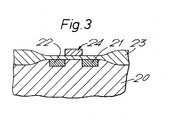
- Fig. 3 illustrates a stage in the method of the present invention.
- source and drain regions 21 and 22 are provided by suitable processing, for example selective diffusion or implantation using the gate as a mask.
- An oxide layer 23 extends over the entire surface of the substrate 20 and as illustrated is thinner in the source, drain gate regions due to the processing involved.
- a gate 24 and interconnects are provided by despositing a layer of silicon rich homogeneous metallic silicide film, by sputtering, for example, of the oxide 23.
- the silicon rich silicide layer is then patterned using dry etching techniques to produce the required gates and interconnects, such as gate 24. No undercutting results from the etching process due to the film homogeneity.
- the composition employed to produce the silicide film is chosen to leave the silicide perfectly formed and of the correct composition after the subsequent conventional oxidation step which uses the excess silicon as a source for oxidation.
- a silicon rich silicide gate structure is deposited so that subsequent oxidation, necessary to form the device, removes the excess silicon leaving a perfectly formed and homogenous silicide.
- the composition comprises a silicon rich silicide containing three silicon atoms to each titanium atom. Such material should support 0.5 ⁇ m of oxide to be grown over an initial silicon rich silicide layer of thickness 0.5 ⁇ m.
- the proposed process provides low interconnect resistance values whilst not disturbing the overall conventional polysilicon-based process significantly.
- the method avoids the etching of heterogeneous layers whilst still retaining the oxidisability of the resultant silicide.
Landscapes
- Electrodes Of Semiconductors (AREA)
- Insulated Gate Type Field-Effect Transistor (AREA)
- Internal Circuitry In Semiconductor Integrated Circuit Devices (AREA)
Applications Claiming Priority (2)
| Application Number | Priority Date | Filing Date | Title |
|---|---|---|---|
| GB8312281 | 1983-05-05 | ||
| GB08312281A GB2139419A (en) | 1983-05-05 | 1983-05-05 | Semiconductor devices |
Publications (1)
| Publication Number | Publication Date |
|---|---|
| EP0124954A2 true EP0124954A2 (de) | 1984-11-14 |
Family
ID=10542196
Family Applications (1)
| Application Number | Title | Priority Date | Filing Date |
|---|---|---|---|
| EP84300674A Withdrawn EP0124954A2 (de) | 1983-05-05 | 1984-02-03 | Halbleiteranordnungen mit Elementen aus Metallsiliziden |
Country Status (3)
| Country | Link |
|---|---|
| EP (1) | EP0124954A2 (de) |
| JP (1) | JPS59207623A (de) |
| GB (1) | GB2139419A (de) |
Cited By (3)
| Publication number | Priority date | Publication date | Assignee | Title |
|---|---|---|---|---|
| FR2578100A1 (fr) * | 1985-02-26 | 1986-08-29 | Efcis | Circuit integre a transistors mos a electrodes en siliciure metallique et procede de fabrication |
| EP0206481A3 (de) * | 1985-05-07 | 1987-08-26 | Hitachi, Ltd. | Halbleiteranordnung mit Mehrschichtbedrahtung |
| US4731318A (en) * | 1985-02-26 | 1988-03-15 | Societe Pour L'etude Et La Fabrication Des Circuits Integres Speciaux - E.F.C.I.S. | Integrated circuit comprising MOS transistors having electrodes of metallic silicide and a method of fabrication of said circuit |
Families Citing this family (6)
| Publication number | Priority date | Publication date | Assignee | Title |
|---|---|---|---|---|
| JPS61168266A (ja) * | 1985-01-21 | 1986-07-29 | Toshiba Corp | Mis型半導体装置の製造方法 |
| JPS61222174A (ja) * | 1985-03-27 | 1986-10-02 | Mitsubishi Electric Corp | 半導体装置の製造方法 |
| JPS61252668A (ja) * | 1985-05-01 | 1986-11-10 | Mitsubishi Electric Corp | 半導体装置の製造方法 |
| JPS6290973A (ja) * | 1985-06-25 | 1987-04-25 | Mitsubishi Electric Corp | 半導体装置の製造方法 |
| JPS625665A (ja) * | 1985-07-02 | 1987-01-12 | Mitsubishi Electric Corp | 半導体装置の製造方法 |
| US5200637A (en) * | 1988-12-15 | 1993-04-06 | Kabushiki Kaisha Toshiba | MOS transistor and differential amplifier circuit with low offset |
Family Cites Families (4)
| Publication number | Priority date | Publication date | Assignee | Title |
|---|---|---|---|---|
| IN140056B (de) * | 1973-11-01 | 1976-09-04 | Rca Corp | |
| IN143383B (de) * | 1974-06-13 | 1977-11-12 | Rca Corp | |
| JPS5780739A (en) * | 1980-11-07 | 1982-05-20 | Hitachi Ltd | Semiconductor integrated circuit device and manufacture thereof |
| JPS596577A (ja) * | 1982-07-05 | 1984-01-13 | Toshiba Corp | 半導体装置とその製造方法 |
-
1983
- 1983-05-05 GB GB08312281A patent/GB2139419A/en not_active Withdrawn
-
1984
- 1984-02-03 EP EP84300674A patent/EP0124954A2/de not_active Withdrawn
- 1984-04-26 JP JP59085075A patent/JPS59207623A/ja active Pending
Cited By (4)
| Publication number | Priority date | Publication date | Assignee | Title |
|---|---|---|---|---|
| FR2578100A1 (fr) * | 1985-02-26 | 1986-08-29 | Efcis | Circuit integre a transistors mos a electrodes en siliciure metallique et procede de fabrication |
| EP0194193A1 (de) * | 1985-02-26 | 1986-09-10 | STMicroelectronics S.A. | Verfahren zum Herstellen eines integrierten Schaltkreises aus MOS-Transistoren mit Elektroden aus Metallsilizid |
| US4731318A (en) * | 1985-02-26 | 1988-03-15 | Societe Pour L'etude Et La Fabrication Des Circuits Integres Speciaux - E.F.C.I.S. | Integrated circuit comprising MOS transistors having electrodes of metallic silicide and a method of fabrication of said circuit |
| EP0206481A3 (de) * | 1985-05-07 | 1987-08-26 | Hitachi, Ltd. | Halbleiteranordnung mit Mehrschichtbedrahtung |
Also Published As
| Publication number | Publication date |
|---|---|
| GB8312281D0 (en) | 1983-06-08 |
| GB2139419A (en) | 1984-11-07 |
| JPS59207623A (ja) | 1984-11-24 |
Similar Documents
| Publication | Publication Date | Title |
|---|---|---|
| US4510670A (en) | Method for the manufacture of integrated MOS-field effect transistor circuits silicon gate technology having diffusion zones coated with silicide as low-impedance printed conductors | |
| US5027185A (en) | Polycide gate FET with salicide | |
| US5302539A (en) | VLSI interconnect method and structure | |
| US5441914A (en) | Method of forming conductive interconnect structure | |
| EP0174773A2 (de) | Halbleiteranordnung mit Verbindungsschichten | |
| JPS62502301A (ja) | 集積回路製造方法 | |
| US5567647A (en) | Method for fabricating a gate electrode structure of compound semiconductor device | |
| US5543362A (en) | Process for fabricating refractory-metal silicide layers in a semiconductor device | |
| EP0124954A2 (de) | Halbleiteranordnungen mit Elementen aus Metallsiliziden | |
| US4968644A (en) | Method for fabricating devices and devices formed thereby | |
| US4563805A (en) | Manufacture of MOSFET with metal silicide contact | |
| EP0124960A2 (de) | Halbleiteranordnungen mit Siliziden | |
| EP0326218A1 (de) | Verfahren zum Herstellen einer Halbleiteranordnung, wobei auf einer Oberfläche eines Halbleiterkörpers eine Metalleiterbahn angebracht wird | |
| EP0068843B1 (de) | Verfahren zum Herstellen eines Leiters mit einem gewünschten Muster auf einem Halbleitersubstrat | |
| US5698468A (en) | Silicidation process with etch stop | |
| US5877085A (en) | Method of manufacturing semiconductor device | |
| US6214710B1 (en) | Method for a semiconductor device having reduced contact resistance and leakage | |
| US6828236B2 (en) | Method for forming silicide wires in a semiconductor device | |
| GB2139418A (en) | Semiconductor devices and conductors therefor | |
| CA1235824A (en) | Vlsi mosfet circuits using refractory metal and/or refractory metal silicide | |
| US6140232A (en) | Method for reducing silicide resistance | |
| US5413968A (en) | Semiconductor device and manufacturing method thereof | |
| JPH03138929A (ja) | シリサイド ゲート レベル ランナ | |
| US4736233A (en) | Interconnect and contact system for metal-gate MOS VLSI devices | |
| US4874720A (en) | Method of making a metal-gate MOS VLSI device |
Legal Events
| Date | Code | Title | Description |
|---|---|---|---|
| PUAI | Public reference made under article 153(3) epc to a published international application that has entered the european phase |
Free format text: ORIGINAL CODE: 0009012 |
|
| AK | Designated contracting states |
Designated state(s): DE FR IT NL |
|
| STAA | Information on the status of an ep patent application or granted ep patent |
Free format text: STATUS: THE APPLICATION HAS BEEN WITHDRAWN |
|
| 18W | Application withdrawn |
Withdrawal date: 19850312 |
|
| RIN1 | Information on inventor provided before grant (corrected) |
Inventor name: TOMKINS, GARY JOHN Inventor name: ROSSER, PAUL JOHN Inventor name: SCOVELL, PETER DENIS |