EP0125156A1 - Kaskadierter Multiplizierer mit einer Anordnung von elementären Operatoren - Google Patents
Kaskadierter Multiplizierer mit einer Anordnung von elementären Operatoren Download PDFInfo
- Publication number
- EP0125156A1 EP0125156A1 EP84400657A EP84400657A EP0125156A1 EP 0125156 A1 EP0125156 A1 EP 0125156A1 EP 84400657 A EP84400657 A EP 84400657A EP 84400657 A EP84400657 A EP 84400657A EP 0125156 A1 EP0125156 A1 EP 0125156A1
- Authority
- EP
- European Patent Office
- Prior art keywords
- operator
- bits
- register
- multiplier
- signal
- Prior art date
- Legal status (The legal status is an assumption and is not a legal conclusion. Google has not performed a legal analysis and makes no representation as to the accuracy of the status listed.)
- Granted
Links
Images


Classifications
-
- G—PHYSICS
- G06—COMPUTING OR CALCULATING; COUNTING
- G06F—ELECTRIC DIGITAL DATA PROCESSING
- G06F7/00—Methods or arrangements for processing data by operating upon the order or content of the data handled
- G06F7/38—Methods or arrangements for performing computations using exclusively denominational number representation, e.g. using binary, ternary, decimal representation
- G06F7/48—Methods or arrangements for performing computations using exclusively denominational number representation, e.g. using binary, ternary, decimal representation using non-contact-making devices, e.g. tube, solid state device; using unspecified devices
- G06F7/52—Multiplying; Dividing
- G06F7/523—Multiplying only
- G06F7/533—Reduction of the number of iteration steps or stages, e.g. using the Booth algorithm, log-sum, odd-even
- G06F7/5334—Reduction of the number of iteration steps or stages, e.g. using the Booth algorithm, log-sum, odd-even by using multiple bit scanning, i.e. by decoding groups of successive multiplier bits in order to select an appropriate precalculated multiple of the multiplicand as a partial product
- G06F7/5336—Reduction of the number of iteration steps or stages, e.g. using the Booth algorithm, log-sum, odd-even by using multiple bit scanning, i.e. by decoding groups of successive multiplier bits in order to select an appropriate precalculated multiple of the multiplicand as a partial product overlapped, i.e. with successive bitgroups sharing one or more bits being recoded into signed digit representation, e.g. using the Modified Booth Algorithm
- G06F7/5338—Reduction of the number of iteration steps or stages, e.g. using the Booth algorithm, log-sum, odd-even by using multiple bit scanning, i.e. by decoding groups of successive multiplier bits in order to select an appropriate precalculated multiple of the multiplicand as a partial product overlapped, i.e. with successive bitgroups sharing one or more bits being recoded into signed digit representation, e.g. using the Modified Booth Algorithm each bitgroup having two new bits, e.g. 2nd order MBA
Definitions
- the present invention relates to multipliers of the cascade type using a set of elementary operators of the same type.
- Each of these elementary operators makes it possible to quickly multiply a binary number (multiplicand) by a small part of another binary number (multiplier).
- multiplicand binary number
- multiplier binary number
- a partial multiplication of rank j between a multiplicand X and a group of two bits Y 2j + 1 Y 2j of the multiplier is done by adding to the previous intermediate result I j-1 one of the five numbers 0, X, 2X, -X, -2X, and by shifting the result S j of this operation by two bits to the right to obtain a new intermediate result 1 1 .
- the choice between these five numbers is made according to the value of the two bits Y 2j + 1 , Y 2j , and of the bit Y 2j + 1 of the previous group, according to the following table:
- the elementary operator represented in FIG. 1 makes it possible to carry out such a partial multiplication between a number X comprising seven bits (including the sign) and two bits Y 2j + 1 and Y 2j of a number Y, ie a 7x2 multiplication with conservation of the sign.
- the operator of FIG. 1 comprises three input registers 101, 102, 103 which make it possible to receive the input data.
- the register 101 includes seven boxes which firstly store the most significant bits of Y not used in the operator j or in those which precede it.
- the boxes freed by the use of the bits of Y make it possible to store the least significant bits of the sum S., which no longer intervene in subsequent partial calculations due to the right shift in the Booth algorithm.
- the register is provided with an output on which there is a copy of the input after the clock step H applied to the register by four delay devices 104 to 107 in series intended to improve the behavior of the circuit.
- the figure represents the case where there are at the input, and therefore at the output, of the register the six most significant bits of Y.
- the register 102 includes nine boxes which make it possible to store the nine most significant bits of the intermediate result I j-1 . This is obtained by shifting two bits to the right of the sum S j-1 at the output of the previous stage and adding two most significant bits equal to the most significant bit of S j-1 . The two least significant bits which overflow in this offset are stored in the register 101 where they replace Y 2j and Y 2j + 1 which arrive in the operator with other inputs.
- the register 102 is also provided with an output which copies its input under the command of H at the output of the delay device 104.
- the register 103 includes ten boxes which make it possible to store the seven bits of the number X, as well as three additional bits. These additional bits include a least significant bit, said to cut. The other two additional bits are two most significant bits which copy the sign bit of X and make it possible during operations to keep this sign. Indeed the 2X (or -2X) operation results in a shift of one bit to the left, and it is moreover necessary to provide for the case where the addition of the signs delivers a carry and therefore requires yet another bit to left.
- This register 103 is also provided with an output which copies its input under the command of H at the output of the delay device 105.
- This output from register 103 is applied to a computing device 108 followed by a multiplexer 109.
- This computing device performs on all ten bits the operations X (direct transfer), X (bit-to-bit complementation of X), 2X (one bit shift to the left), and 2X (complementation followed by a left shift).
- Multiplexer 109 selects the result of one of these four operations under the control of two binary signals which respectively represent Y 2j + 1 and B. These signals are obtained in a manner described below.
- the multiplexer is designed to select only the nine most significant bits, thereby eliminating the cross-over bit which was used in the multiplication by 2 and which is then no longer useful.
- the number at the output of the multiplexer 109 is added to I j-1 , available at the output of the register 102, in a nine-bit adder 110.
- This adder is provided with an input and a carry output.
- adding 1 by the carry input gives -X and -2X in addition to 2, which is the code used.
- the output of the adder, and I j-1, are applied to a multiplexer 111 which selects one of these two signals under control of the signal A, obtained as explained later, and outputs the S signal. .
- the two bits Y 2j-1 and Y 2j coming from the previous stage, are applied to an OR-exclusive gate 112 which delivers the signal B defined above.
- This signal B is stored in a master-slave flip-flop 113 to be applied to the multiplexer 109. This flip-flop is controlled by the clock H at the output of the delay device 107.
- the bit Y 2j + 1 from the previous stage is stored in a master-slave flip-flop 114 to be applied to the multiplexer 109.
- This flip-flop is controlled by the clock H directly.
- the two bits Y 2j and Y 2j + 1 are also applied to an exclusive OR gate 115 whose output is connected to an OR gate 116.
- the other input of this gate receives the signal B, and its output delivers the signal A defined above.
- This signal A is stored in a master-slave flip-flop 117 to be applied to the multiplexer 111. This flip-flop is controlled by the clock H at the output of the delay device 106.
- the signals X and Y 2j + 1 necessary for the next stage, are available at the output of the register 103 and the flip-flop 114, with the delay of a clock step which corresponds to the loading of the register and the flip-flop.
- the same is true for the signals Y 2j + 2 and Y 2j + 3 (contained in Y) and Si.
- X has been represented on nine bits, which includes the two bits of sign SX.
- the cross bit R is not available, because there is no use in transmitting it.
- Such an operator can be integrated in a pre-distributed integrated circuit of commerce, contained in a single box.
- the invention proposes a cascade type multiplier using a set of elementary operators, each elementary operator having a first register Y for receiving and delivering a first signal of at least two bits and at most m bit (m 7 ), a second register RI to receive an intermediate signal of n bits, a third register X to receive a multiplicand signal of n bits and a cross-bit and to deliver this multiplicand signal, decoding circuits D and Q to receive a multiplier signal of three bits and deliver the most significant bit of this signal, a nine-bit adder provided with a carry-in input and a carry-out output, and a circuit S for delivering a nine-bit multiplication signal obtained according to the Booth algorithm between the multiplicand, the intermediate signal and the multiplier, mainly characterized in that, to carry out at least one multiplication between a multiplicand of 2 (n-1) bits and a multiplier of qu other bits, it comprises a first stage comprising a first operator and a second operator and a second stage comprising
- FIG. 2 shows the first stage of a 16x16 multiplier between two signed integers.
- This multiplier therefore performs a 16 ⁇ 2 multiplication between a number X comprising 16 bits X 0 to X 15 , and the first two bits Y 0 and Y of a number Y comprising 16 bits Y 0 to Y 15 .
- This stage comprises two identical operators numbered 0 and 1.
- the internal diagram of these operators is that of FIG. 1 and to facilitate the understanding of the drawing, the input and output circuits are represented diagrammatically by dividing into two parts some of the them (X, Y, 110).
- the operator who works on the least significant of the multiplicand, receives on its input register X the nine least significant bits X 0 to X 8 applied to the inputs of the X register other than that of overlap.
- the input R of the cross-over bit is kept at zero to have a least significant bit at zero in the case of a left shift.
- the operator 0 also receives on its input register RI the nine least significant bits I 0 to I 8 of the intermediate result of the preceding stage, which in this case are at zero since we describe the first stage.
- the first two least significant bits Y o and Y of the multiplier (actually used in this stage) are applied to the various decoding circuits detailed in FIG. 1 and gathered in FIG. 2 in an input circuit called D.
- Y I is also applied to the retaining input of the adder of operator 0.
- Circuit D should also receive a bit Y -1 . Since this does not exist, we substitute a Q bit which is kept at zero.
- Operator 1 which works on the most significant of the multiplicand, receives on its input register X the eight most significant bits X 8 to X 15 .
- X 9 to X 15 are applied to the seven least significant entries and X 15 , which represents the sign, is copied to the two most significant entries for the reasons given in the description of the operator.
- X 8 is applied to the input of the cross-over bit, which explains more particularly the interest of this bit. Indeed if one carries out a shift on the left (representing a multiplication by 2), it is necessary to have the preceding bit on the right since this shift operates on the totality of the number, which is present in two pieces in the two operators.
- the operator 1 also receives on its input register RI the nine most significant bits 1 9 to 1 17 (in this case zero), and on its input register Y the seven most significant bits Y 9 to Y 15 , which are transmitted on the output of this register.
- bits Y 0 and Y 1 are applied to operator 1 in the same way as to operator 0, except for the incoming carry which receives the outgoing carry bit from l operator 0, which ensures continuity between the two pieces of the multiplication.
- this operator 1 we find, in addition to Y 9 to Y 15 already seen, the seven most significant bits X 9 to X 15 and the two additional sign bits, the nine most significant bits S 1 0 to S 1 8 of the result of the 16x2 multiplication, and the bit Y 1 .
- the carry output is available, but is not useful here since it represents the sign of the result, which is already contained at least once in the number output from S.
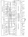
- Figure 3 There is shown in Figure 3 the cascading of a second stage comprising two operators 2 and 3, with the first stage of Figure 1, shown partially, to be able to perform a 16x4 multiplication.
- This second stage therefore uses the three bits Y 1 to Y 3 of the multiplier, which are applied to the circuits D of the two operators, with Y 3 applied in addition to the carry input of operator 2.
- Y 2 and Y 3 are taken at the output of the register Y of the operator 0, and in the version represented Y 1 at the output respectively of the two circuits Q of the operators 0 and 1.
- Possible variants would consist in connecting the output of one of these circuits Q to two corresponding inputs of circuits D.
- the outputs of the X registers of the first stage are directly connected to the inputs of the X registers of the second stage, since the multiplicand is transmitted without change along the stages with simply the delay d0 at each stage. Likewise, the input R of operator 2 is kept at zero.
- the intermediate result corresponding to the multiplication by one digit of the multiplier must be shifted by one digit to the right before being added to the next intermediate result. So the number formed of bits S 0 0 to S 1 8 must be shifted by two bits to the right (since the first stage used two bits of the multiplier) to be transmitted to the second stage.
- the two bits S 0 0 and S 0 1 which form the two least significant bits M O and M 1 of the final result are stored in the two most significant stages of the register Y of the operator 3, bringing together the starters and corresponding outputs. These two stages are released by shifting the multiplicand by two bits to the right, by first connecting the outputs Y 11 to Y 15 of operator 1 to the five least significant inputs of register Y of operator 3, then by connecting the outputs Y 10 and Y9 of this operator 1, and Y 8 to Y 4 of operator 0, to the inputs of register Y of operator 2.
- Y 3 and Y 2 are used in circuits D for the calculation, and therefore no longer have to be transmitted to the registers Y of the second stage.
- Y 4 to Y 10 available at the output of the Y register of the operator 2, and Y 11 to Y 15 with M 0 and M 1 at the output of the Y register of the operator 3. Furthermore Y 3 (necessary for the third stage) is available at the output of the two Q circuits of the second stage, as we have seen.
- I 0 to I 8 are applied to the input register RI of operator 2, and I 9 to I 15 to the input register RI of operator 3.
- I 9 to 1 15 represent only seven bits, I 15 is also copied over the two most significant entries of this latter register.
- the result of the 16 ⁇ 4 multiplication performed by these two stages is composed of the two least significant bits M 0 and M 1 already seen, and of the most significant 18 bits S 2 0 to S 2 8 and S 3 0 to S 3 8 available. at the output of the registers S of the two operators of the second stage.
- the two bits Y 2j + 3 and Y 2j + 2 necessary for the multiplication in the stage j + 1, are taken at the output of the register Y of the operator j of least significant weight, and the set of the remaining bits of Y, as well as the result bits M already obtained, are shifted to the right by two steps to be applied at the input of the registers Y of stage j + 1. This frees up space on the left for the two new least significant bits of the result at the output of circuits S of stage j.
Landscapes
- Physics & Mathematics (AREA)
- General Physics & Mathematics (AREA)
- Engineering & Computer Science (AREA)
- Computational Mathematics (AREA)
- Mathematical Analysis (AREA)
- Mathematical Optimization (AREA)
- Pure & Applied Mathematics (AREA)
- Theoretical Computer Science (AREA)
- Computing Systems (AREA)
- General Engineering & Computer Science (AREA)
- Complex Calculations (AREA)
Applications Claiming Priority (2)
| Application Number | Priority Date | Filing Date | Title |
|---|---|---|---|
| FR8305600A FR2544105B1 (fr) | 1983-04-06 | 1983-04-06 | Multiplieur du type en cascade utilisant un ensemble d'operateurs elementaires |
| FR8305600 | 1983-04-06 |
Publications (2)
| Publication Number | Publication Date |
|---|---|
| EP0125156A1 true EP0125156A1 (de) | 1984-11-14 |
| EP0125156B1 EP0125156B1 (de) | 1988-06-22 |
Family
ID=9287563
Family Applications (1)
| Application Number | Title | Priority Date | Filing Date |
|---|---|---|---|
| EP19840400657 Expired EP0125156B1 (de) | 1983-04-06 | 1984-04-03 | Kaskadierter Multiplizierer mit einer Anordnung von elementären Operatoren |
Country Status (3)
| Country | Link |
|---|---|
| EP (1) | EP0125156B1 (de) |
| DE (1) | DE3472313D1 (de) |
| FR (1) | FR2544105B1 (de) |
Cited By (1)
| Publication number | Priority date | Publication date | Assignee | Title |
|---|---|---|---|---|
| FR2611286A1 (fr) * | 1987-02-23 | 1988-08-26 | Dassault Electronique | Circuit integre multiplieur, et son procede de composition |
Citations (3)
| Publication number | Priority date | Publication date | Assignee | Title |
|---|---|---|---|---|
| US4065666A (en) * | 1976-10-15 | 1977-12-27 | Rca Corporation | Multiply-divide unit |
| US4122527A (en) * | 1975-11-04 | 1978-10-24 | Motorola, Inc. | Emitter coupled multiplier array |
| US4130878A (en) * | 1978-04-03 | 1978-12-19 | Motorola, Inc. | Expandable 4 × 8 array multiplier |
-
1983
- 1983-04-06 FR FR8305600A patent/FR2544105B1/fr not_active Expired
-
1984
- 1984-04-03 DE DE8484400657T patent/DE3472313D1/de not_active Expired
- 1984-04-03 EP EP19840400657 patent/EP0125156B1/de not_active Expired
Patent Citations (3)
| Publication number | Priority date | Publication date | Assignee | Title |
|---|---|---|---|---|
| US4122527A (en) * | 1975-11-04 | 1978-10-24 | Motorola, Inc. | Emitter coupled multiplier array |
| US4065666A (en) * | 1976-10-15 | 1977-12-27 | Rca Corporation | Multiply-divide unit |
| US4130878A (en) * | 1978-04-03 | 1978-12-19 | Motorola, Inc. | Expandable 4 × 8 array multiplier |
Non-Patent Citations (2)
| Title |
|---|
| IEEE JOURNAL OF SOLID-STATE CIRCUITS, vol. SC-18, no. 2, avril 1983, pages 204-210, IEEE, New York, US; H. YAMAUCHI et al.: "10 ns 8 x 8 multiplier LSI using super self-aligned process technology" * |
| NACHRICHTEN ELEKTRONIK, vol. 36, no. 3, mars 1982, pages 106-119, Heidelberg, DE; V. LEESEMANN: "Seriell/Parallel-Multiplizierer für die digitale Signalverarbeitung, Teil 2" * |
Cited By (1)
| Publication number | Priority date | Publication date | Assignee | Title |
|---|---|---|---|---|
| FR2611286A1 (fr) * | 1987-02-23 | 1988-08-26 | Dassault Electronique | Circuit integre multiplieur, et son procede de composition |
Also Published As
| Publication number | Publication date |
|---|---|
| EP0125156B1 (de) | 1988-06-22 |
| FR2544105B1 (fr) | 1988-10-14 |
| FR2544105A1 (fr) | 1984-10-12 |
| DE3472313D1 (en) | 1988-07-28 |
Similar Documents
| Publication | Publication Date | Title |
|---|---|---|
| EP0712071B1 (de) | Verfahren zur Verwendung der modularen Multiplikation nach der Montgomery-Methode | |
| TWI263402B (en) | Reconfigurable fir filter | |
| EP0223657B1 (de) | Rechnungseinrichtung von diskreter Fouriertransformation und seine Anwendung auf einem Radarsystem | |
| FR2489554A1 (fr) | Circuit de traitement numerique en arithmetique distribuee utilisant des multiplexeurs a l'entree d'une memoire | |
| EP0437876B1 (de) | Programmierbarer serieller Multiplikator | |
| EP0692762A1 (de) | Logikschaltung zur parallelen Multiplikation | |
| EP0171305B1 (de) | Rechenschaltung für die diskrete Fouriertransformation | |
| EP0259231B1 (de) | Vorrichtung zur Ermittlung der digitalen Transformation eines Signals | |
| FR2624282A1 (fr) | Comparateur binaire et operateur de tri de nombres binaires | |
| EP0237382B1 (de) | Gerät zur Kosinustransformation eines abgetasteten digitalen Signals | |
| US8046401B2 (en) | Canonical signed digit multiplier | |
| EP0125156B1 (de) | Kaskadierter Multiplizierer mit einer Anordnung von elementären Operatoren | |
| EP0476592A2 (de) | Adressengenerator für den Datenspeicher eines Prozessors | |
| EP0020185A1 (de) | Verfahren und Vorrichtung zur seriell-parallelen Addition einer grossen Anzahl von Wörtern | |
| FR2796736A1 (fr) | Procede pour effectuer une multiplication avec accumulation dans un corps de galois | |
| EP0190514B1 (de) | On-line-Testeinrichtung für einen Rechnerkreis der diskreten Fouriertransformation und Kreis der eine solche Einrichtung enthält | |
| EP0327445A1 (de) | Allgemeiner digitaler Multiplizierer und digitaler Filter mit diesem Multiplizierer | |
| EP0175623A1 (de) | Einrichtung zur Echtzeitdigitalsignalverarbeitung durch Faltung | |
| EP0112768B1 (de) | Elementärer Operator, insbesondere für Multiplizierer vom Kaskadetyp | |
| EP0122843B1 (de) | Modularer Integrator | |
| CA2359198C (fr) | Unite de calcul pour l'execution d'un protocole cryptographique | |
| FR2517915A1 (fr) | Dispositif de matricage pour camera de television en couleurs et codeur et camera comportant un tel dispositif | |
| KR100451193B1 (ko) | 필터회로 | |
| FR2536541A1 (fr) | Systeme simplifie d'analyse spectrale a exploitation de phase | |
| FR2666861A1 (fr) | Generateur d'adresses pour la memoire de donnees d'un processeur. |
Legal Events
| Date | Code | Title | Description |
|---|---|---|---|
| PUAI | Public reference made under article 153(3) epc to a published international application that has entered the european phase |
Free format text: ORIGINAL CODE: 0009012 |
|
| AK | Designated contracting states |
Designated state(s): DE GB IT NL |
|
| 17P | Request for examination filed |
Effective date: 19850131 |
|
| 17Q | First examination report despatched |
Effective date: 19860422 |
|
| GRAA | (expected) grant |
Free format text: ORIGINAL CODE: 0009210 |
|
| AK | Designated contracting states |
Kind code of ref document: B1 Designated state(s): DE GB IT NL |
|
| ITF | It: translation for a ep patent filed | ||
| GBT | Gb: translation of ep patent filed (gb section 77(6)(a)/1977) | ||
| REF | Corresponds to: |
Ref document number: 3472313 Country of ref document: DE Date of ref document: 19880728 |
|
| PG25 | Lapsed in a contracting state [announced via postgrant information from national office to epo] |
Ref country code: GB Effective date: 19890403 |
|
| PLBE | No opposition filed within time limit |
Free format text: ORIGINAL CODE: 0009261 |
|
| STAA | Information on the status of an ep patent application or granted ep patent |
Free format text: STATUS: NO OPPOSITION FILED WITHIN TIME LIMIT |
|
| RAP4 | Party data changed (patent owner data changed or rights of a patent transferred) |
Owner name: THOMSON-CSF |
|
| 26N | No opposition filed | ||
| PG25 | Lapsed in a contracting state [announced via postgrant information from national office to epo] |
Ref country code: NL Effective date: 19891101 |
|
| GBPC | Gb: european patent ceased through non-payment of renewal fee | ||
| NLV4 | Nl: lapsed or anulled due to non-payment of the annual fee | ||
| PG25 | Lapsed in a contracting state [announced via postgrant information from national office to epo] |
Ref country code: DE Effective date: 19900103 |