EP0125699A2 - Datenausgabeanordnung für einen dynamischen Speicher - Google Patents
Datenausgabeanordnung für einen dynamischen Speicher Download PDFInfo
- Publication number
- EP0125699A2 EP0125699A2 EP84105570A EP84105570A EP0125699A2 EP 0125699 A2 EP0125699 A2 EP 0125699A2 EP 84105570 A EP84105570 A EP 84105570A EP 84105570 A EP84105570 A EP 84105570A EP 0125699 A2 EP0125699 A2 EP 0125699A2
- Authority
- EP
- European Patent Office
- Prior art keywords
- node
- output
- data
- nodes
- mosfets
- Prior art date
- Legal status (The legal status is an assumption and is not a legal conclusion. Google has not performed a legal analysis and makes no representation as to the accuracy of the status listed.)
- Withdrawn
Links
- 230000015654 memory Effects 0.000 claims abstract description 18
- 230000008859 change Effects 0.000 claims description 7
- 239000003990 capacitor Substances 0.000 claims description 5
- 230000008878 coupling Effects 0.000 claims description 2
- 238000010168 coupling process Methods 0.000 claims description 2
- 238000005859 coupling reaction Methods 0.000 claims description 2
- 238000010586 diagram Methods 0.000 description 22
- 230000006870 function Effects 0.000 description 6
- 239000004065 semiconductor Substances 0.000 description 5
- 230000003111 delayed effect Effects 0.000 description 3
- 230000004888 barrier function Effects 0.000 description 2
- 230000002093 peripheral effect Effects 0.000 description 2
- 230000015572 biosynthetic process Effects 0.000 description 1
- 230000015556 catabolic process Effects 0.000 description 1
- 238000006731 degradation reaction Methods 0.000 description 1
- 230000001934 delay Effects 0.000 description 1
- 230000009467 reduction Effects 0.000 description 1
Images


Classifications
-
- G—PHYSICS
- G11—INFORMATION STORAGE
- G11C—STATIC STORES
- G11C11/00—Digital stores characterised by the use of particular electric or magnetic storage elements; Storage elements therefor
- G11C11/21—Digital stores characterised by the use of particular electric or magnetic storage elements; Storage elements therefor using electric elements
- G11C11/34—Digital stores characterised by the use of particular electric or magnetic storage elements; Storage elements therefor using electric elements using semiconductor devices
- G11C11/40—Digital stores characterised by the use of particular electric or magnetic storage elements; Storage elements therefor using electric elements using semiconductor devices using transistors
- G11C11/401—Digital stores characterised by the use of particular electric or magnetic storage elements; Storage elements therefor using electric elements using semiconductor devices using transistors forming cells needing refreshing or charge regeneration, i.e. dynamic cells
- G11C11/4063—Auxiliary circuits, e.g. for addressing, decoding, driving, writing, sensing or timing
- G11C11/407—Auxiliary circuits, e.g. for addressing, decoding, driving, writing, sensing or timing for memory cells of the field-effect type
- G11C11/409—Read-write [R-W] circuits
- G11C11/4096—Input/output [I/O] data management or control circuits, e.g. reading or writing circuits, I/O drivers or bit-line switches
Definitions
- the present invention relates to a data output circuit for a dynamic memory device with a nibble mode function.
- dynamic memory devices are mainly used because the use of such memory devices requires less transistors for making a memory cell.
- Some of the dynamic memories, particularly large capacity memories, for example, 256 Kilo bits have a nibble mode function in order to speed up the read-out and write operation.
- the 256 Kilo bits memory device with the nibble mode function is constructed, as shown in Fig. 1, to have four memory cell groups Ca - Cd each consisting of 64 Kilo.bits.
- the memory cells of 64 Kilo bits in each of the cell groups Ca - Cd are selectively accessed by 8-bit row addresses A OR - A 7R and 8-bit column addresses A OC - A 7C .
- a ROW ADDRESS STROBE (RAS) and a COLUMN ADDRESS STROBE (CAS) cooperate to specify addresses (x, y) of the memory cell groups Ca - Cd.
- the contents in the memory cells located at the specified addresses are read out and latched in a latch section, or a 4-bit latch Lh.
- the contents of the 4-bit latch Lh are sequentially and cyclically read out through a read register Rr.
- the read,out data is produced as output data Dout.
- a program counter Pc specifies a specific one bit in the 4-bit latch Lh. While receiving the most signigicant bit (MSB) A 8R of the row address signal and the MSB ABC of the column address signal, the program counter Pc cyclically performs the counting operation according to a change of the logical value of the CAS. By the count of the program counter Pc, a specific one bit is selected from those in the 4-bit latch counter Lh.
- a selector Sr selects either the read out register Rr'or the write register Wr according to an operation mode of the semiconductor memory device, either a read mode or a write mode.
- Fig. 2 shows timing diagrams illustrating a read cycle of the semiconductor memory device.
- a row address is given by an address signal AO - A8, applied during an effective period to indicate that the RAS is low or L in logical level.
- a column address is given by an address signal AO - A8, applied during an effective period to indicate that the CAS is L.
- the row and column addresses are selected by these signals. Then, every time the CAS changes in logical level, the contents in the bit stages of the 4-bit latch Lk are sequentially and cyclically read out from the memory cells of the semiconductor memory device. In the read operation, the memory cell, as specified by the row address A 8R and the column address A 8C , is first read out.
- a write mode of the semiconductor memory device is executed according to timing diagrams shown in Fig. 3.
- a row address is given by an address signal AO - A8, as applied during an effective period, to indicate that the RAS is L.
- a column address is given by an address signal AO - A8, as applied during an affective period to indicate that the CAS is L.
- a write signal ( WRITE ) is effected and the write operation is performed every time the signal CAS changes.
- the data is replaced from d to f, a to g, b to h, e to i, f to j, g to k, b to h, i to m, j to n and k to o.
- the finally replaced data is written into the memory cell in each of the cell groups Ca - Cd as specified by the row address signal and the column address signal, and the data already stored is discarded. Therefore, the contents of the memory cells in the cell groups Ca - Cd, corresponding to the cells a - d in the 4-bit latch Lh, are o, 1, m, and n, respectively.
- the dynamic memory device with such a nibble mode function, by changing the CAS at short periods while keeping the RAS at L, it can read out or write the contents of the 4-bit latch Lh at a high speed in synchronism with the CAS , without changing the address.
- Fig. 4 shows a circuit diagram illustrating an arrangement of one bit stage of the conventional 4-bit latch Lh.
- latch line pairs I/0 and I/0 are respectively connected to paired output lines DO and DO , through series circuits containing MOSFETs 1 - 4 and 5 - 8.
- the gates of the MOSFETs 1 and 2 are wired together and to the latch line I/0 .
- the gates of the MOSFETs 5 and 6 are wired together and to the latch line I/O.
- a series connection point of the MOSFETs 1 and 2 and a series connection point of the MOSFETs 5 and 6 are interconnected through a node N1.
- the node N1 is connected through a MOSFET 9 to a power source V SS .
- a clock pulse ⁇ L is applied to the gate of the MOSFET 9.
- the MOSFETs 2 and 3 are series connected to provide a node N2.
- the MOSFETs 6 and 7 are series connected to provide a node N3.
- the gates of MOSFETs 3 and 7 as a first transistor pair are wired together.
- a clock pulse ⁇ g is applied to the interconnected gates of the first transistor pair.
- the MOSFETs 3 and 4 are series connected to provide a node N4, and the MOSFETs 7 and 8 are series connected and provide a node N5.
- the gates of the MOSFETs 4 and 8 as a second transistor pair are connected together.
- a select signal R is applied to the interconnected gates of the second transistor pair.
- the read register Rr succeeding the 4-bit latch register Lh thus arranged, contains a MOSFET 10, inserted between the output line pair DO and DO , and MOSFETs 11 and 12, inserted between the power sources V DD , with the MOSFET 10 interposing therebetween.
- a clock pulse ⁇ p is applied to the gates of these MOSFETs 10 - 12.
- a level on the latch line pair 1/0 and I/O is forced to be changed according to the write data.
- the clock ⁇ g is placed in a L level to turn off the first transistor pair of the MOSFETs 3 and 7, in order that levels on the latch output line pair DO and DO remain unchanged.
- the latch line pair 1/0 and I/O are precharged up to a potential of the power source V DD when the RAS is H, as shown in a timing chart of F ig. 5 .
- the clock ⁇ p is V p ( > V DD + V T )
- the latch output line pair DO and DO are precharged up to V DD by a combination of the MOSFETs 10 - 12.
- the CAS falls, data from the memory cell is transferred to the latch line pair I/O and I/O , so that the latch line pair has a logical level as given by the contents of the data transferred.
- the clock ⁇ L rises and the node N1 is coupled with a power source V SS .
- the contents of data causes one of the MO SFETs 1 and 5 constituting a flip-flop to turn on.
- the data causes one of the MOSFETs 2 and 6 to turn on.
- the nodes N1 - N3 are charged at a voltage V DD - V T at the prechanging time where the RAS is H .
- the clock pulse ⁇ g rises up to a potential Vp, and slightly later a select signal R also rises. Accordingly, the nodes N2 and N4 are connected to the output line D0, while the nodes N3 and N5 are connected to the output line DO . Under this condition, one of the latch output lines DO and DO is discharged according to the data held by the flip-flop made up of the MOSFETs 1 and 5. At the same time, the other is in a floating state and keeps a precharge level.
- one of the output lines DO and DO is connected to the power source V SS and its potential is reliably fixed at that potential.
- the other is in a floating state and if it is connected to another node, charges on this output line are shared with the node.
- the potential on the output line drops or is greatly changed by charge leakage or the like.
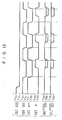
- Fig. 6 shows a timing diagram exaggeratedly illustrating a read cycle in the nibble mode.
- valid data is output after a predetermined time t NCAC following the fall of the column address strobe signal CAS .
- the valid data terminates after a predetermined time toff following the rise of the column address strobe signal CAS .
- time delays t NCAC and toff are determined by the associated circuit.
- a cycle time t NC can be set at a proper value if it is larger than a minimum value t NCmin which depends on minimum values t NCPmin of a precharge time t NCP and t NCASmin of a pulse width t NCAS of the column address strobe signal CAS for guaranteeing a circuit operation.
- a valid data period of the output data Dout is important, that is, a width of a data window.
- a memory device with a large data window is very easy to use because the design on the data transfer between the memory device and the peripheral circuit suffers from less design restrictions.
- To widen the data window it is sufficient to enlarge the pulse width t NCAS of the column address strobe signal CAS. This results in an elongation of the cycle time t NC .
- the elongated cycle time t NC degrades the high speed performance as a useful feature of the nibble mode function. Ideally, it is desired that a maximum data window be gained within a minimum cycle time.
- the period of the data window can be enlarged up to the cycle time tNC, if desired.
- a reduction of the time toff, if done, can be at most approximately the minimum value t NCQmin of the precharge period. Therefore, a practical maximum value of the data window is approximately t NCAS - t NCAC + t CPmin . This indicates that when the memory device is operated with the minimum cycle time t NCmin , the data window is approximately t NCmin - t NCAC and is very small.
- Another way to enlarge the data window is to further elongate the time toff.
- the clock pulse used in the precharging system is used for resetting the data output circuit. Therefore, if the time toff is set at large value, the reset clock pulse must be greatly delayed behind the rise of the column address strobe signal CAS. If an extremely short precharge time t NCP is set, the reset clock pulse fails to rise, and the read operation enters into the next read cycle. To avoid this, it is necessary increase the minimum value t NCPmin during the precharge period. The result is an enlargement of the minimum value t NCmin of the cycle time and a degradation of the high speed performance associated with the nibble mode function.
- Fig. 7 there is shown a circuit diagram of the data output section of the read register Rr.
- three MOSFETs 11 - 12 connected in series fashion, are connected at both ends to the power source V DD .
- the series connection points of these MOSFETs are respectively coupled with paired output lines DO and DO of the latch circuit.
- the paired output lines DO and DO are respectively connected through the MOSF ETs 13 and 14 to the power source V SS . Further, those output lines are respectively connected to the gates of the MOSFETs 17 and 18, through the MOSFETs 15 and 16 and nodes N6 and N7.
- a precharge clock ⁇ p is applied to the MOSFETs 10 - 12.
- the gates of the MOSFETs 15 and 16 are connected together to the power source V DD .
- Drive signals ⁇ out are respectively connected to the power supply V SS through the series paths of the MOSFETs 17 and 19 and of the MOSFETs 18 and 20.
- the gate of the MOSFET 13 is connected to the power source V SS through the node N8 and the MOSFET 21.
- a precharge clock ⁇ p is applied to the gate of the MOSFET 21.
- the gate of the MOSFET 13 is connected to the gates of the MOSFETs 20 and 22 and to a series connection point of the MOSFETs 17 and 19.
- the gate of the MOSFET' 14 is connected to the power source V SS through the MOSFET 23, of which the gate is impressed with a precharge clock pulse ⁇ p.
- the gate of the MOSFET 14 is connected to the gates of the MOSFETs 19 and 24 and a series connection point of the MOSFETs 18 and 20.
- the MOSFETs 24 and 22 as respectively the load transistor and the drive transistor are connected in series between the power sources V DD and V SS .
- Output data is derived from a data output node Output, or a series connection point of these transistors 24 and 22.
- the read register Rr with such a circuit arrangement operates in a sequence as shown in Fig. 8.
- the precharge clock ⁇ p is V p ( > V DD + V T )
- the paired output lines DO and DO in the latch circuit are at V DD level.
- a potential at the node N6 between the MOSFETs 15 and 17 is V DD -V T .
- a potential at the node N7 between the MOSFETs 16 and 18 is also V DD - V T .
- the node N8, associated with the gate of the MOSFET 22, and the node N9, associated with the MOSFET 24, are at potential of V SS . Under this condition, the MOSFETs 22 and 24 are turned off and the output node Output of the read register is at a high impedance.
- the precharge clock signal ⁇ p is also L.
- the nodes N6 and N7 are placed at the potential according to the applied data.
- the output clock ⁇ out rises up to Vp
- the nodes N8 and N9 are at Vp level according to the data.
- Potentials at the nodes N8 and N9 are fed back to the output line pair DO and DO , through the MOSFETs 13 and 14, thereby ensuring the data transfer.
- one of the MOSFETs 22 and 24 is turned on and the output node Output is at V DD or V SS .
- the precharge clock ⁇ p rises too.
- the nodes N8 and N9 are both at V SS , and the output node Output is at a high impedance. In this case, to make the time toff long, it is sufficient to delay the rise of the precharge clock ⁇ p.
- the rise of the precharge clock ⁇ p is delayed too much, it can not rise within the precharge cycle of the column address strobe signal CAS , as indicated by ⁇ R' in Fig. 8. Further, the output line pair DO and DO of the latch circuit are not precharged. As a result, it is impossible to transfer data in the succeeding fall cycle of the column address strobe signal CAS.
- the delay of the time toff is limited within the time period allowing the precharge clock ⁇ p to rise. This implies that the elongation of the time toff must be approximately within the minimum value t NCPmin of the precharge time period. For this reason, an insufficient width of the data window can be obtained.
- an object of the present invention is to provide a data output circuit for a dynamic memory device having a data output section capable of widening a data window period up to approximately a minimum cycle t NCmin , and a latch section for reliably fixing potentials on paired output lines of a latch circuit by respectively coupling the paired output lines to the power sources V SS and V DD at the time of data outputting.
- a data output circuit for a dynamic memory device which can reliably keep the potentials on the paired output lines of a latch circuit, and which has a wide data window; hence, facilitating the interface of the memory device with a peripheral circuit. It is thereby capable of making the best use of the high speed performance essential to the nibble mode.
- a data output section for a dynamic memory device which is an embodiment of the present invention, will be described referring to Fig. 9.
- MOSFETs 35 and 36 are respectively inserted between series connection points of MOSFETs 30 - 32 and MOSFETs 33 and 34.
- a gate clock pulse ⁇ g is applied to the gates of the MOSFETs 35 and 36.
- the MOSFETs 33 and 34 are connected together at a node N10 and a MOSFET 37 which is further connected to ground.
- An output clock ⁇ out is applied to the gate of the MOSFET 37.
- a gate clock pluse ⁇ g is applied through a MOSFET 38 to a node N11 between the MOSFETs 35 and 33.
- a precharge clock ⁇ p is applied to the gate of the MOSFET 38.
- a gate clock pulse ⁇ g is applied through a MOSFET 39 to a node N12 as a series connection point of the MOSFETs 34 and 36.
- a precharge clock ⁇ p is applied to the gate of the MOSFET 39.
- a node N13 is continuous to a MOSFET 40 which is coupled at one end to an output clock ⁇ out.
- a node N14 is continuous to a MOSFET 41 which is coupled at one end to an output clock ⁇ out.
- the gate of the MOSFET 40 is connected to a node N11 through a node N15 and a MOSFET 42.
- the gate of the MOSFET 41 is connected to the node N12 through a node N16 and a MOSFET 43.
- the gates of the MOSFETs are connected together to the power source V DD .
- the node N13 is connected to the power source V SS through MOSFETs 44 and 45.
- a reset clock pulse ⁇ R is applied to the gate of the MOSFET 44.
- the gate of the MOSFET 45 is connected to the node N14.
- the node N14 is connected to the power source V SS through the MOSFETs 46 and 47.
- a reset clock pulse ⁇ R is applied to the gate of the MOSFET 46.
- the gate of the MOSFET 47 is connected to the node N13.
- MOSFETs 48 and 49 respectively as load and drive transistors are connected in series between the power sources V DD and V SS . An output signal Output is derived from a series connection point of these transistors 48 and 49.
- the precharge clock ⁇ p is at V DD + V T ; where V DD is the power voltage and V T is a threshold voltage of the MO SF E T.
- the reset clock pulse ⁇ R is at V DD .
- the latch output line pair DO and DO are charged to the potential of the power source V DD since the MOSFETs 30 - 32 are in an ON state.
- the nodes N11 - 16 except the output line pair DO and DO and the node N10 are at the potential of the power source V SS because the MOSFETs, of which the gates are applied with either the precharge clock ⁇ p or the reset clock pulse ⁇ R , is turned on and the clock pluses ⁇ g and ⁇ out are at V SS .
- the node N10 is in a floating state. Therefore, the output signal Output is disconnected from both the power sources V DD and V SS'
- the gate clock pluse ⁇ g rises up to the potential of the power source V DD , while the precharge clock ⁇ p and the reset clock pulse ⁇ R both fall. Then, the MOSFETs 35 and 36 are turned on, while the MOSFETs 30 - 32, 38, and 39 are turned off.
- the charges stored in the output line DO of the latch circuit are distributed into the nodes N12 and N16.
- the charges stored in the DO are distributed into the nodes N11 and N15.
- the paired output lines DO and DO and the nodes N11, N12, N15, and N16 are at a medium potential V M .
- the capacitance of the paired output line DO or DO is generally larger than that at the nodes N12 and N16 or N11 and N15. Therefore, the medium potential V M is higher than the threshold voltage of the MOSFETs 40 and 41, and hence turns on these transistors.
- the capacitance of the output line DO or DO is smaller than the capacitance of the nodes N12 and N16 or N11 and N15, it is necessary to additionally use a proper capacitor for the output line DO or DO .
- the nodes N13 and N14 are coupled with an output circuit drive signal ⁇ out which is at the potential of the power source V SS , and keeps the potential V SS as given in the precharge phase. Therefore, the output signal Output is disconnected from both the power sources V SS and V DD .
- the output line DO is coupled with the power source V DD and the output line DO with the power source V SS .
- the potential at the nodes N16 and N12 is V DD - V T
- the potential at the nodes N15 and N11 is V SS - V T
- the drive signal ⁇ out rises to the potential Vp
- the node N16 is coupled with the drive signal ⁇ out and rises to the potential of Vp because of the presence of the barrier MOSFET 43.
- the node N14 is also at the potential Vp of the drive signal ⁇ out.
- the MOSFET 37 is turned on, and hence the MOSFET 33 is turned on.
- the output line DO and the nodes N15 and N11 are connected to the potential V SS .
- the gate of the MOSFET 48 is at Vp level to allow the output signal Output to be connected to the potential of the power source VDD. In this way, the data on the output line DO is output from the output node Output.
- the gate clock pluse ⁇ g falls to the potential of the power source V SS , and the precharge clock ⁇ p rises up to the potential Vp. Accordingly, the MOSFETs 38 and 39 are turned on, and the nodes N16 and N12, and N15 and N11 are at the V SS level. And the MOSFETs 40 and 41 are turned off. Accordingly, if the drive signal ⁇ out then falls to the potential V SS , the nodes N13 and N14 keep the previous potential levels. Therefore, the potential Vp at the node N14 is kept at its level.
- the MOSFETs 30 - 32 are turned on, and the output line pair DO and DO are precharged at level V DD .
- the precharge time t NCP is the minimum cycle approximate to the minimum value t NCPmin , which is within a tolerable range in the design of this circuit.
- the column address strobe signal CAS falls before the reset clock pulse ⁇ R rises.
- the reset clock pulse ⁇ R fails to rise, and the MOSFETs 44 and 46 are left in an OFF state.
- this circuit is designed such that the reset clock pulse ⁇ R is delayed in its rise to elongate the time toff and to widen the data window.
- the MOSFET 48 is in an ON state, and the output node Output continues the output of data.
- the gate clock pulse ⁇ g rises to the potential of the power source V DD
- the precharge clock ⁇ p falls to the potential of the power source VSS.
- the MOSFETs 35 and 36 are turned on, the output line pair DO and DO and the nodes N16, N12, N15, and N11 are all at the same medium potential level V M .
- the MOSFETs 40 and 41 are turned on and the output drive circuit signal ⁇ out at the potential V SS is coupled with the nodes N13 and N14, thereby to change the potential on the node N14 from the V p to V SS'
- the reset clock pulse ⁇ R rises to the potential of the power source V DD since the precharge time is sufficiently large. Then, the MOSFETs 44 and 46 are turned on and the nodes N13 and N14 are connected to the power source V SS' thereby to turn on the MOSFETs 48 and 49. Then, the output node Output is disconnected from both the power sources V DD and V SS and the data output is stopped.
- the precharge clock pulse ⁇ p and the gate clock pulse ⁇ g are so timed as to have a period in which both are H. During this period, the charges in the output line pair DO and DO are discharged.
- the particular circuit under discussion applies the gate clock pulse ⁇ g through the MOSFETs 38 and 39 to the nodes N11 and N12. Therefore, when the precharge clock ⁇ p and the gate clock pulse ⁇ g are not simultaneously "H", the nodes of the MOSFETs 38 and 39, to which the gate clock pluse ⁇ g is applied, may be connected to the power source V SS .
- a clock pulse changing like the gate clock pulse ⁇ g, may be used for the gate clock pulse ⁇ g.
- the signal ⁇ out input to the gate of the MOSFET 37 may also be replaced by a signal which is pulsed from low to high before the signal ⁇ out rises and pulsed from a high to a low of the V SS before the gate clock pulse ⁇ g rises.
- the nibble mode operation is performed in the following manner with the minimum cycle t NCmin and the precharge time t NCPmin , when the column address strobe signal CAS rises following the row address strobe signal RAS , as shown in a timing diagram of Fig. 11.
- an Output 1 indicates a waveform of the output signal from the conventional data output section for a dynamic memory device.
- the data output section is reset by the clock signal ⁇ l in the precharge system which rises following the sequence of operations associated with the precharge on an internal node, which follows the rise of the column address strobe signal CAS. Therefore, the data output section is not reset until the clock ⁇ 1 rises. In other words, the data output section can not produce the data before the signal ⁇ 1 rises. As a result, the dat window is much shorter than the minimum cycle t NCmin .
- An output 2 in Fig. 11 illustrates a waveform of the output signal from the data output section, as shown in Fig. 9.
- a reset clock pulse ⁇ R is used in the precharge system for resetting this circuit.
- the reset clock pulse ⁇ R rises, after a long delay, behind the rise of the column address strobe signal CAS. Because of this, it can not rise within the cycle of the minimum nibble mode.
- the data output section normally operates since it is reset by making use of the charged stored at the time of precharge to the output line pair DO and DO . Further, the data window is extended to approach the minimum cycle t NCmin . Therefore, the data output circuit of Fig. 9 can make the best use of the high speed performance essential to the nibble mode, while requiring less design restrictions on the signal timings in the circuit operation.
- the node In the data output section shown in Fig. 9, the node must be charged by the output signal from the high level line of those line pairs DO and DO .
- the conventional latch section As shown in Fig. 4, one of the paired output lines DO and DO is wired to the power source V SS , while the other is in a high floating level. Therefore, the output line in the high level operates in an unstable floating level.
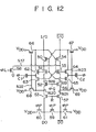
- a latch circuit as shown in Fig. 12, is desirably used as the latch circuit for applying a signal through the paired output lines DO and DO to the data output circuit, as shown in Fig. 9..
- Fig. 12 at the time of data is being output, one of the output lines DO and DO is connected to the power source V DD , while the other is connected to the power source V SS , thereby reliably fixing the potentials on the respective output lines.
- Fig. 12 shows a circuit diagram illustrating a latch section according to the present invention.
- a pair of latch lines 1/0 and I/O are respectively connected through MOSFETs 50 - 53 and MOSFETs 54 - 57 to a pair of output lines DO and DO of the latch circuit.
- the gates of the MOSFETs 50 and 51 are connected together and to the latch line I/O .
- the gates of the MOSFETs 54 and 55 are connected together and to the latch line 1/0.
- a series connection point of the MOSFETs 50 and 51 and a series connection point of the MOSFETs 54 and 55 are continuous to a node N17 further connected to the power source V SS through a MOSFET 58.
- the gate of the MOSFET 58 is impressed with a clock pulse ⁇ L .
- the MOSFETs 51 and 52 are interconnected to provide a node N18.
- the MOSFETs 55 and 56 are interconnected to provide a . node N19.
- a gate clock pulse ⁇ g is coupled to an interconnection of the gates of the MOSFETs 52 and 56.
- Interconnections between the MOSFETs 52 and 53 and between the MOSFETs 56 and 57 respectively provide nodes N20 and N21.
- a second pair of the transistor MOSFETs 53 and 57 are interconnected at the gates. The interconnection of the gates is impressed with a select signal R.
- MOSFET 59 is interposed between the output line pair DO and DO , and further MOSFETs 60 and 61, connected in series, are connected at both ends to the power source V DD .
- a precharge clock pulse ⁇ p is deposited to the gates of the MOSFETs 59 - 61.
- MOSFETs 62 and 63 are serially placed between the latch line I/O and a node N20.
- the gates of the MOSFETs 62 and 63 are respectively coupled with the paired latch lines I/O and I/O.
- the MOSFETs 64 and 65 are serially placed between the latch line I/O and a node N21.
- the gates of the MOSFETs 64 and 65 are respectively coupled with the paired latch lines I/O and I/O .
- MOSFETs 66 and 67, as first charging transistors, are respectively inserted between the paired latch lines I/O and I/O and the power source VDD, as shown.
- Second charge transistors, or MOSFETs 68 and 69 are respectively placed between the nodes N20 and N21 and the power source V DD' as shown.
- a junction point between the MOSFETs 62 and 63 and a junction point between the gates of MOSFETs 66 and 68 are interconnected through a node N22.
- a clock pulse ⁇ is capacitively coupled with a node N22, through a capacitor Cl.
- a junction point between the MOSFETs 64 and 65 and a junction point between the gates of MOSFETs 6 7 and 69 are interconnected through a node N23.
- the node N23 is applied with a clock pulse ⁇ through a capacitor C2.
- the paired I/O line has been charged up to the potential of the power source VDD.
- the latch line pair I/O and I/O are at the potential of the power source V DD . Accordingly, the MOSFETs 50, 54, 51, 55, 62, 64, 63, and 65 are turned on to cause the nodes N17 - N23 to be at V DD - V T .
- the precharge clock pulse ⁇ p falls to the potential of the power source V SS .
- the MOSFETs 59 - 61 are turned off and the output line pair DO and DO float.
- data is output to the latch line pair I/O and I/O .
- the clock pulse ⁇ L goes positive to turn on the MOSFET 58.
- the node 17 is connected to the potential of the power source V SS , and the MOSFETs 50 and 54 form a flip-flop.
- the potential on the latch line I/O is dropped to the level of the V SS power supply through the MOSFET 54. Then, the MOSFETs 50, 51, 62 and 65 are turned off. With the turning off of the MOSFET 50, the latch line I/O retains a high level. With the turning off of the MOSFET 62, the node N22 is isolated from the latch line I/O. As the result of turning off the MOSFET 51, the node N18 is isolated from the node N17, thus keeping its high level.
- the V SS power supply potential on the latch line I/O causes the nodes N19 and N23 to be placed at the same potential.
- the MOSFETs 52 and 56 are on, and the node N21 is continuous to the node N19 to ensure the potential of the V SS power supply. Then, when the clock pulse ⁇ rises, the capacitor Cl boosts the level on the node N22. At this time, the gate of the MOSFET 63 is approximately at the potential of the V DO power supply and the node N20 is approximately V DD - V T . Under this condition, the MOSFET 63 operates as a barrier, so that the potential on the node N22 is pulled up to Vp.
- the Vp on the node N22 turns on the MOSFETs 66 and 68 to connect the latch line I/O to the V DO power supply and to connect the node N20 to the potential of the V DD power supply. Even if the clock pulse ⁇ goes positive, the node N23 is left low in potential because it is connected to the V SS power supply.
- the select signal R rises up to Vp and the MOSFETs 53 and 57 are turned on. Further, the output line DO is connected to the node N20, and through the MOSFET 53 to the V DD power supply. Finally, the output line DO is fixed at the potential of the V DD power supply.
- the output line DO is connected to the potential of the V SS power supply through the MOSFETs 55 - 57. Subsequently, the gate clock pulse ⁇ g falls to the potential of the V SS power supply, turning off the MOSFETs 52 and 56. Then, the writing operation is performed to reverse the potentials on the latch lines I/O and I/O . Accordingly, the latch line I/O is connected to the V SS power supply, and the latch line I/O is connected to the V DD power supply. With the connection, logical states in the flip-flop including the MOSFETs 50 and 54 are forcibly inverted.
- the MOSFETs 63, 54, 55, and 64 are off, while the MOSFETs 65, 50, 51, and 62 are on.
- the node N23 is disconnected from the latch line I/O and connected to the node N21 since the MOSFET 64 is off and the MOSFET 65 is on.
- the node N22 is disconnected from the node N20 and connected to the latch'line I/O since the MOSFET 62 is on and the MOSFET 63 is off.
- the result is that the node N22 is at the potential of the V SS power supply, the MOSFETs 66 and 68 are off, and the latch line 1/0 and the node N20 are disconnected from the V DD power supply.
- the column address strobe signal CAS goes positive, and the precharge clock pulse ⁇ p goes positive and reaches Vp.
- the MOSFETs 59 - 61 are turned on, and the output lines DO and DO are coupled to the V DD power supply.
- the clock pulse ⁇ goes negative, but the select signal R is still at Vp. Therefore, the nodes N20 and N21 are at V DD .
- the node N 2 3 connected to the node N21 is charged up to V DD V T .
- the node N22 is connected to the V SS power supply, via the MOSFETs 50, 58 and 62.
- one of the nodes N20 and N21 is connected to the V DD power supply according to the potentials on the nodes N22 and N23.
- the above operation is performed in the respective latch sections. Accordingly, if the latch selected and the output line pair DO and DO are interconnected, one of the output lines DO and DO is always connected the V DD power supply, while the other is always connected to the V SS power supply, according to the data held in the latch section.
- A(DO, DO ) illustrates a variation of the signal levels on the output line pair in the prior art.
- the high level portions indicate a floating state.
- B(D0, DO) shows a variation of the signal level on the output line pair in the embodiment of the present invention. As shown, the potential on the output line pair is held at V DD or V SS .
- the high level output line drops its potential when the column address strobe signal CAS falls and the data output section operates, even if the output lines are charged up to the V DD potentials in the precharge time.
- the reason for this is that in such a situation, charges on the high level output line are divided because the other node is charged.
- the high level output line of those DO and DO is connected to the V D power supply at the leading edge of the clock pulse ⁇ , so that its high level can reliably be held.
- the MOSFETs in the above-mentioned embodiment may of course be replaced by ordinary transistors.
- the data window can be widened, for example, up to about the minimum cycle t NCmin , thereby making the best use of the high speed performance of the nibble mode.
Landscapes
- Engineering & Computer Science (AREA)
- Databases & Information Systems (AREA)
- Microelectronics & Electronic Packaging (AREA)
- Computer Hardware Design (AREA)
- Dram (AREA)
- Static Random-Access Memory (AREA)
Applications Claiming Priority (4)
| Application Number | Priority Date | Filing Date | Title |
|---|---|---|---|
| JP86057/83 | 1983-05-17 | ||
| JP58086057A JPS59213089A (ja) | 1983-05-17 | 1983-05-17 | デ−タラツチ回路 |
| JP246311/83 | 1983-12-27 | ||
| JP58246311A JPS60138797A (ja) | 1983-12-27 | 1983-12-27 | ダイナミツクメモリのデ−タ出力回路 |
Publications (2)
| Publication Number | Publication Date |
|---|---|
| EP0125699A2 true EP0125699A2 (de) | 1984-11-21 |
| EP0125699A3 EP0125699A3 (de) | 1986-10-08 |
Family
ID=26427222
Family Applications (1)
| Application Number | Title | Priority Date | Filing Date |
|---|---|---|---|
| EP84105570A Withdrawn EP0125699A3 (de) | 1983-05-17 | 1984-05-16 | Datenausgabeanordnung für einen dynamischen Speicher |
Country Status (2)
| Country | Link |
|---|---|
| US (1) | US4603403A (de) |
| EP (1) | EP0125699A3 (de) |
Cited By (4)
| Publication number | Priority date | Publication date | Assignee | Title |
|---|---|---|---|---|
| EP0144223A3 (en) * | 1983-12-01 | 1986-10-08 | Fujitsu Limited | Semiconductor memory device |
| EP0254065A3 (de) * | 1986-06-25 | 1990-07-04 | Nec Corporation | Halbleiterspeicher vom Adressenmultiplex-Typ |
| EP0269106A3 (en) * | 1986-11-27 | 1990-07-04 | Kabushiki Kaisha Toshiba | Semiconductor memory device |
| KR100934065B1 (ko) * | 2004-12-31 | 2009-12-24 | 비와이디 컴퍼니 리미티드 | 리튬 이온 이차전지용 전해질 |
Families Citing this family (30)
| Publication number | Priority date | Publication date | Assignee | Title |
|---|---|---|---|---|
| GB8401804D0 (en) * | 1984-01-24 | 1984-02-29 | Int Computers Ltd | Data storage apparatus |
| JPS61110399A (ja) * | 1984-11-05 | 1986-05-28 | Toshiba Corp | ダイナミツクメモリのデ−タ出力回路 |
| US4766572A (en) * | 1984-12-27 | 1988-08-23 | Nec Corporation | Semiconductor memory having a bypassable data output latch |
| US4908796A (en) * | 1988-05-24 | 1990-03-13 | Dallas Semiconductor Corporation | Registered outputs for a memory device |
| JP2534782B2 (ja) * | 1989-11-10 | 1996-09-18 | 株式会社東芝 | 半導体装置 |
| DE69122293T2 (de) * | 1990-04-27 | 1997-04-24 | Nippon Electric Co | Halbleiterspeicheranordnung |
| JP2683176B2 (ja) * | 1991-10-30 | 1997-11-26 | 川崎製鉄株式会社 | 読出し専用記憶装置 |
| US5352937A (en) * | 1992-11-16 | 1994-10-04 | Rca Thomson Licensing Corporation | Differential comparator circuit |
| US6804760B2 (en) | 1994-12-23 | 2004-10-12 | Micron Technology, Inc. | Method for determining a type of memory present in a system |
| US5682354A (en) * | 1995-11-06 | 1997-10-28 | Micron Technology, Inc. | CAS recognition in burst extended data out DRAM |
| US5729503A (en) * | 1994-12-23 | 1998-03-17 | Micron Technology, Inc. | Address transition detection on a synchronous design |
| US6525971B2 (en) | 1995-06-30 | 2003-02-25 | Micron Technology, Inc. | Distributed write data drivers for burst access memories |
| US5652724A (en) * | 1994-12-23 | 1997-07-29 | Micron Technology, Inc. | Burst EDO memory device having pipelined output buffer |
| US5610864A (en) * | 1994-12-23 | 1997-03-11 | Micron Technology, Inc. | Burst EDO memory device with maximized write cycle timing |
| US5668773A (en) * | 1994-12-23 | 1997-09-16 | Micron Technology, Inc. | Synchronous burst extended data out DRAM |
| US5526320A (en) * | 1994-12-23 | 1996-06-11 | Micron Technology Inc. | Burst EDO memory device |
| US5598376A (en) * | 1994-12-23 | 1997-01-28 | Micron Technology, Inc. | Distributed write data drivers for burst access memories |
| US5675549A (en) * | 1994-12-23 | 1997-10-07 | Micron Technology, Inc. | Burst EDO memory device address counter |
| US5640364A (en) * | 1994-12-23 | 1997-06-17 | Micron Technology, Inc. | Self-enabling pulse trapping circuit |
| US5721859A (en) * | 1994-12-23 | 1998-02-24 | Micron Technology, Inc. | Counter control circuit in a burst memory |
| US5717654A (en) * | 1995-02-10 | 1998-02-10 | Micron Technology, Inc. | Burst EDO memory device with maximized write cycle timing |
| US5850368A (en) * | 1995-06-01 | 1998-12-15 | Micron Technology, Inc. | Burst EDO memory address counter |
| US5729504A (en) * | 1995-12-14 | 1998-03-17 | Micron Technology, Inc. | Continuous burst edo memory device |
| US7681005B1 (en) * | 1996-01-11 | 2010-03-16 | Micron Technology, Inc. | Asynchronously-accessible memory device with mode selection circuitry for burst or pipelined operation |
| US5966724A (en) * | 1996-01-11 | 1999-10-12 | Micron Technology, Inc. | Synchronous memory device with dual page and burst mode operations |
| US6401186B1 (en) | 1996-07-03 | 2002-06-04 | Micron Technology, Inc. | Continuous burst memory which anticipates a next requested start address |
| US6981126B1 (en) * | 1996-07-03 | 2005-12-27 | Micron Technology, Inc. | Continuous interleave burst access |
| US7103742B1 (en) | 1997-12-03 | 2006-09-05 | Micron Technology, Inc. | Burst/pipelined edo memory device |
| JP2002082830A (ja) * | 2000-02-14 | 2002-03-22 | Mitsubishi Electric Corp | インターフェイス回路 |
| US7927948B2 (en) | 2005-07-20 | 2011-04-19 | Micron Technology, Inc. | Devices with nanocrystals and methods of formation |
Family Cites Families (4)
| Publication number | Priority date | Publication date | Assignee | Title |
|---|---|---|---|---|
| US4250412A (en) * | 1979-03-05 | 1981-02-10 | Motorola, Inc. | Dynamic output buffer |
| JPS5625290A (en) * | 1979-08-07 | 1981-03-11 | Nec Corp | Semiconductor circuit |
| JPS56101694A (en) * | 1980-01-18 | 1981-08-14 | Nec Corp | Semiconductor circuit |
| DE3243496A1 (de) * | 1982-11-24 | 1984-05-24 | Siemens AG, 1000 Berlin und 8000 München | Integrierte halbleiterschaltung mit einem dynamischen schreib-lese-speicher |
-
1984
- 1984-05-16 EP EP84105570A patent/EP0125699A3/de not_active Withdrawn
- 1984-05-16 US US06/610,781 patent/US4603403A/en not_active Expired - Lifetime
Cited By (4)
| Publication number | Priority date | Publication date | Assignee | Title |
|---|---|---|---|---|
| EP0144223A3 (en) * | 1983-12-01 | 1986-10-08 | Fujitsu Limited | Semiconductor memory device |
| EP0254065A3 (de) * | 1986-06-25 | 1990-07-04 | Nec Corporation | Halbleiterspeicher vom Adressenmultiplex-Typ |
| EP0269106A3 (en) * | 1986-11-27 | 1990-07-04 | Kabushiki Kaisha Toshiba | Semiconductor memory device |
| KR100934065B1 (ko) * | 2004-12-31 | 2009-12-24 | 비와이디 컴퍼니 리미티드 | 리튬 이온 이차전지용 전해질 |
Also Published As
| Publication number | Publication date |
|---|---|
| US4603403A (en) | 1986-07-29 |
| EP0125699A3 (de) | 1986-10-08 |
Similar Documents
| Publication | Publication Date | Title |
|---|---|---|
| US4603403A (en) | Data output circuit for dynamic memory device | |
| US4685089A (en) | High speed, low-power nibble mode circuitry for dynamic memory | |
| US4567579A (en) | Dynamic memory with high speed nibble mode | |
| US3953839A (en) | Bit circuitry for enhance-deplete ram | |
| EP0045063B1 (de) | Speicheranlage | |
| EP0171518B1 (de) | Pufferschaltung für RAM-Speicher | |
| US4161040A (en) | Data-in amplifier for an MISFET memory device having a clamped output except during the write operation | |
| US4322635A (en) | High speed serial shift register for MOS integrated circuit | |
| US5198999A (en) | Serial input/output semiconductor memory including an output data latch circuit | |
| EP0329910A1 (de) | Zweistufiger Leserverstärker für RAM-Speicher | |
| US4087704A (en) | Sequential timing circuitry for a semiconductor memory | |
| EP0096421B1 (de) | Statische Speicheranordnung mit einem Signalübergangsdetektor | |
| EP0120033A4 (de) | Schaltung im seriendatenbetrieb für einen speicher. | |
| KR900008938B1 (ko) | 반도체 메모리 장치 | |
| EP0056240A2 (de) | Speicheranordnung | |
| US6337821B1 (en) | Dynamic random access memory having continuous data line equalization except at address translation during data reading | |
| US4710904A (en) | Constant pulse width generator including transition detectors | |
| US3938109A (en) | High speed ECL compatible MOS-Ram | |
| JPS61175994A (ja) | メモリのデコ−ド・ドライブ回路 | |
| US4831590A (en) | Semiconductor memory including an output latch having hysteresis characteristics | |
| US4447892A (en) | Pre-charge for the bit lines of a random access memory | |
| US4742487A (en) | Inhibit and transfer circuitry for memory cell being read from multiple ports | |
| EP0062547A2 (de) | Speicherschaltung | |
| EP0325105A1 (de) | Multiport-Speicher | |
| US4485461A (en) | Memory circuit |
Legal Events
| Date | Code | Title | Description |
|---|---|---|---|
| PUAI | Public reference made under article 153(3) epc to a published international application that has entered the european phase |
Free format text: ORIGINAL CODE: 0009012 |
|
| 17P | Request for examination filed |
Effective date: 19840516 |
|
| AK | Designated contracting states |
Designated state(s): DE FR GB |
|
| PUAL | Search report despatched |
Free format text: ORIGINAL CODE: 0009013 |
|
| AK | Designated contracting states |
Kind code of ref document: A3 Designated state(s): DE FR GB |
|
| 17Q | First examination report despatched |
Effective date: 19880118 |
|
| STAA | Information on the status of an ep patent application or granted ep patent |
Free format text: STATUS: THE APPLICATION IS DEEMED TO BE WITHDRAWN |
|
| 18D | Application deemed to be withdrawn |
Effective date: 19880531 |
|
| RIN1 | Information on inventor provided before grant (corrected) |
Inventor name: TODA, HARUKIC/O PATENT DIVISION |