EP0126371A2 - Appareil de mémoire à disque souple - Google Patents
Appareil de mémoire à disque souple Download PDFInfo
- Publication number
- EP0126371A2 EP0126371A2 EP84105165A EP84105165A EP0126371A2 EP 0126371 A2 EP0126371 A2 EP 0126371A2 EP 84105165 A EP84105165 A EP 84105165A EP 84105165 A EP84105165 A EP 84105165A EP 0126371 A2 EP0126371 A2 EP 0126371A2
- Authority
- EP
- European Patent Office
- Prior art keywords
- floppy disk
- signal
- magnetic head
- circuit
- generating
- Prior art date
- Legal status (The legal status is an assumption and is not a legal conclusion. Google has not performed a legal analysis and makes no representation as to the accuracy of the status listed.)
- Withdrawn
Links
Images



Classifications
-
- G—PHYSICS
- G11—INFORMATION STORAGE
- G11B—INFORMATION STORAGE BASED ON RELATIVE MOVEMENT BETWEEN RECORD CARRIER AND TRANSDUCER
- G11B19/00—Driving, starting, stopping record carriers not specifically of filamentary or web form, or of supports therefor; Control thereof; Control of operating function ; Driving both disc and head
- G11B19/20—Driving; Starting; Stopping; Control thereof
-
- G—PHYSICS
- G11—INFORMATION STORAGE
- G11B—INFORMATION STORAGE BASED ON RELATIVE MOVEMENT BETWEEN RECORD CARRIER AND TRANSDUCER
- G11B5/00—Recording by magnetisation or demagnetisation of a record carrier; Reproducing by magnetic means; Record carriers therefor
- G11B5/48—Disposition or mounting of heads or head supports relative to record carriers ; arrangements of heads, e.g. for scanning the record carrier to increase the relative speed
- G11B5/54—Disposition or mounting of heads or head supports relative to record carriers ; arrangements of heads, e.g. for scanning the record carrier to increase the relative speed with provision for moving the head into or out of its operative position or across tracks
- G11B5/55—Track change, selection or acquisition by displacement of the head
- G11B5/5521—Track change, selection or acquisition by displacement of the head across disk tracks
- G11B5/5526—Control therefor; circuits, track configurations or relative disposition of servo-information transducers and servo-information tracks for control thereof
- G11B5/553—Details
Definitions
- the present invention relates to a floppy disk drive apparatus.
- a floppy disk drive apparatus which shifts a magnetic head in the radial direction of a floppy disk fitted over a spindle, while rotating the floppy disk, and a data write/read operation is effected with respect to the floppy disk.
- the floppy disk drive apparatus of this type is adapted to control the operation of a motor for rotating the spindle and pulse motor for linearly moving a magnetic head, and is connected to a host computer for effecting a data write/read operation with respect to the floppy disk through the magnetic head.
- the apparatus includes a detector for optically detecting that the magnetic head is placed in a reference track position or a track zero position and is adapted to supply a track zero sinal to the host computer when motor drive signals in a predetermined phase relation are supplied to the pulse motor while an output signal is being generated from the detector. Since, in this case, the detector optically detects the position of the magnetic head, it cannot detect the track zero position of the magnetic head accurately.
- the pulse motor is a four-phase motor which is driven, for example, according to a 2-phase excitation method to cause the head to be moved by one track each time the phase of the motor drive signal varies, the motor drive signal comes to have the same phase relation each time the magnetic head is moved by four tracks.
- a floppy disk drive apparatus comprising a control signal generating circuit for generating a step signal and direction instruction signal, a first drive section for rotating a floppy disk, a second drive section for causing a carrier to which a magnetic head is attached to be driven in the radial direction of the floppy disk in response to the step signal and direction instruction signal, a detecting circuit for generating an output signal when it detects that the magnetic head is placed in the outer limit location of the floppy disk, and an inhibiting circuit for inhibiting the detecting circuit from generating an output signal in response to the direction instruction signal generated from the control signal generating circuit to move the magnetic head in the inner direction of the floppy disk.
- a track zero signal is generated only when the magnetic head is driven in the outer peripheral direction of the floppy disk and reaches a track zero position, and is inhibited from being generated when the magnetic head is driven in the inner direction of the floppy disk.
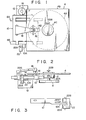
- Figs. 1 and 2 are a schematic top plan view and a side elevational view illustrating a floppy disk drive apparatus according to one embodiment of the present invention.
- This floppy disk driving apparatus comprises a spindle 2 for holding a floppy disk 4; a motor 6 for rotating this spindle 2; two fixed shafts 8A and 8B; a head carrier 10 slidably attached on these shafts 8A and 8B; and a motor 12 for driving this head carrier 10 along the shafts 8A and 8B throuth a pulley 14.
- the floppy disk 4 has a disk medium 4A and a casing 4B for enclosing this disk medium 4A.
- An index hole 4C is formed in this floppy disk 4, while a long hole 4D extending in the radial direction of the disk medium 4A is formed in the casing 4B.
- a magnetic head 16 and a pressure-contacting member 18 for pressing the disk medium 4A onto the magnetic head 16 through the long holes 4D are attached on and over the head carrier 10.
- this floppy disk drive apparatus has an index sensor formed of a light emitting diode 20A and a phototransistor 20B for generating an output signal when the index hole 4C of the floppy disk 4 is detected; and outer peripheral limit location detector 22 for generating an inhibition signal to a motor control circuit (not shown) for driving the motor 12 when a projecting portion 10A of the carrier 10 is detected, thereby inhibiting the movement of the carrier 10 out of a predetermined range.
- This outer peripheral limit location detector 22 is constituted by a light emitting diode 22A and a phototransistor 22B.
- Fig. 3 shows the positional relationship between the outer peripheral limit location detector 22 and the carrier 10. This detector 22 generates an output signal when light emitted from the light emitting diode 22A to the phototransistor 22B is interrupted by the projecting portion 10A of the carrier 10.
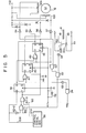
- Fig. 4 is a circuit diagram of a control circuit of a floppy disk drive apparatus according to one embodiment of the present invention.
- a light emitting diode 22A is energized by a current supplied from a power supply terminal +V through a resistor R1 and emits the light.
- the emitter of the phototransistor 22B is grounded and the collector is connected to the power supply terminal +V through a resistor R2.
- the collector of the phototransistor 22B is also connected to one input terminal of an AND gate 30 through a buffer 32.
- the output terminal of the AND gate 30 is connected to one input terminal of the AND gate 34 which is connected at the other input terminal to a Q output terminal of a flip-flop 36 operating as a latch circuit.
- a direction instruction signal DIR from a control signal generating circuit 38 is supplied to the D input terminal of the flip-flop 36.
- a step signal STP from the control signal generating circuit 38 is supplied to a T input terminal of the flip-flop 36 directly, and to T input terminals of flip-flops 40 and 42, through an integrating circuit 44.
- An output terminal of an exclusive OR gate 46 whose one input terminal is connected to a Q output terminal of the flip-flop 42 is coupled to a D input terminal of the flip-flop 40.
- an output terminal of an exclusive OR gate 48 whose one input terminal is connected to a Q output terminal of the flip-flop 40 is coupled to a D input terminal of the flip-flop 42.
- a Q output terminal of the flip-flop 36 is connected to the other input terminal of these exclusive OR gates 46 and 48.
- the Q output terminals of the flip-flops 40 and 42 are respectively connected to input terminals of an AND gate 50 whose output terminal is connected to the other input terminal of the AND gate 30.
- an initial reset circuit 52 is connected to reset terminals of the flip-flops 36, 40 and 42.
- Q and Q output signals from the flip-flop 42 are supplied as motor drive signals ⁇ A and ⁇ C and Q and Q output signals of the flip-flop 40 are supplied as motor drive signals ⁇ B and ⁇ D to the stepping motor 12.
- the motor drive signals ⁇ A and ⁇ C are supplied through inverters 54 and 55 to respective ends of an energizing coil 12A of the stepping motor 12, and the motor drive signals ⁇ B and ⁇ D are supplied through inverters 56 and 57 to respective ends of an energizing coil 12B of the stepping motor 12.
- the center taps of the energizing coils 12A and 12B are each connected to the power source terminal +V2.
- the output states of the flip-flops 40 and 42 are changed in response to the pulse signal STP, causing the logic state of the drive signals ⁇ A , ⁇ B , ⁇ C , and ⁇ D to be changed in accordance with a predetermined sequence. Due to this, the motor 12 is rotated for example in the forward direction and the head 16 is driven in the outer peripheral direction of the floppy disk 4. When the magnetic head 16 reaches near the outer peripheral limit location of the floppy disk 4 and the light from the light emitting diode 22A to the phototransistor 22B is interrupted by the projecting portion 10A of the carrier 10, the phototransistor 22B is rendered nonconductive, so that a "1" level signal is supplied from the buffer 32 to the AND gate 30.
- the rotation of the motor 12 in the forward direction is inhibited and it is inhibited that the magnetic head 16 is further driven in the outer peripheral direction of the floppy disk 4, so that the magnetic head 16 is stopped in the outer peripheral limit location.
- the direction instruction signal DIR from the control signal generating circuit 38 is changed to the "1" level in this state and the control signal generating circuit 38 starts to generate the step signal STP.
- the flip-flop 36 is set to the "1" output state in response to the step signal STP.
- the step signal STP from the control signal generating circuit 38 is supplied through the integrating circuit 44 to the trigger terminals of the flip-flops 40 and 42, thereby allowing these flip-flops 40 and 42 to be set into the "1" and "0" output states, respectively.
- the step signal is generated from the control signal generating circuit 38, the output states of the flip-flops 40 and 42 are changed and the logic state of the drive signals ⁇ A , ⁇ B , ⁇ C and ⁇ D are changed in accordance with the sequence different from that in the former case. Due to this, the motor 12 is rotated reversely and the magnetic head 16 is driven in the inner peripheral direction of the floppy disk 4.
- a track zero signal TRo is generated when the magnetic head 16 is moved in the outer peripheral direction of the floppy disk 4 and reaches the track zero position, and is inhibited from being generated when the magnetic head 16 is moved in the inner direction of the floppy disk.
- the flip-flop 36 is set to an output state, corresponding to the direction instruction signal DIR, in response to the step signal STP.
- the flip-flop 36 is held in an output state "0" irrespective of the level of a direction instruction signal from the control signal generating circuit 38. Unless, in this case, the step signal is generated, it is possible to continue the generation of the track zero signal TRo from the AND gate 34 without holding the direction instruction signal DIR at the "0" level.
- Fig. 5 shows a control circuit of a floppy disk drive apparatus according to another embodiment of the present invention.
- the control circuit of this embodiment is substantially the same as that of Fig. 4, except that use is made of a logic circuit 60 for controlling a step signal STP from the control signal generating circuit 38 and that exclusive OR gates 47 and 49 are used in place of exclusive OR gates 46 and 48.
- the Q output terminals of flip-flop circuits 36 and 42 are connected to the input terminals of the exclusive OR gate 47, and the Q and Q output terminals of the flip-flops 36 and 40, respectively, are connected to the input terminals of the exclusive OR gate 49.
- the Q output terminal of the flip-flop 36 is connected to one input terminal of an AND gate 34 through an inverter 62.
- the logic circuit 60 includes a NAND gate 60-1 having one input terminal connected to the output terminal of an AND gate 30 and the other input terminal connected to receive a direction instruction signal DIR which is supplied from a control signal generating circuit 38 through an inverter 60-2, and an AND gate 60-3 having one input terminal connected to receive an output signal of the NAND gate 60-1, the other input terminal connected to receive a step signal STP from the control signal generating circuit 38, and an output terminal connected to the trigger terminals of the flip-flop 36, 40 and 42.
- the control signal generating circuit 38 when the magnetic head 16 is moved in the outer direction of the floppy disk 4, the control signal generating circuit 38 produces a step signal STP and a "0" level direction instruction signal DIR.
- a "0" level signal is generated from the AND gate 30
- a "1" level signal is generated from the NAND gate 60-1
- the step signal STP is supplied to the trigger terminals of the flip-flops 36, 40 and 42 through the AND gate 60-3.
- the stepping motor 12 is rotated in the forward direction to permit the magnetic head 16 to be moved in the outer direction of the floppy disk.
- the AND gate 30 When, in this way, the magnetic head 16 reaches the track zero position, the AND gate 30 produces a "1" level signal. By so doing, a "0" level signal is generated from the NAND gate 60-1, causing the AND gate 60-3 to be disabled, thus inhibiting a supply of the step signal STP to the flip-flops 36, 40 and 42. As a result, even if the step signal STP continues to be generated from the control signal generating circuit 38, the stepping motor 12 is no longer rotated in the forward direction,
- Fig. 6 is a block diagram of a floppy disk drive apparatus according to still another embodiment of the present invention.
- This floppy disk drive apparatus has a central processing unit (CPU) 100; a read only memory (ROM) 102 and a random access memory (RAM) 104 which are coupled to this CPU 100 through a data bus; and a control signal generating circuit 106 coupled to the CPU 100 through an interface 108.
- the motors 6 and 12, outer peripheral limit location detector 22 and an index sensor 109 are coupled to the CPU 100 through motor drivers 110 and 112 and I/O ports 114 and 115, respectively.
- the RA M 104 has a memory area Ml for storing the data to inhibit that the magnetic head 16 is driven in the inner peripheral direction immediately after the power supply is turned on; memory areas MA, MB, MC, and MD for storing the data corresponding to the drive signals ⁇ A , ⁇ B , ⁇ C and D; and a memory area M2 for storing the data representing the track position of the floppy disk 4 where the magnetic head 16 exists.
- the control signal generating circuit 106 generates the step signal STP and direction instruction signal DIR which are necessary to drive the motor 12, and a motor control signal necessary to drive the motor 6 and the like in response to key signals from, e.g., an external keyboard circuit.
- the CP U 100 executes a main routine such as shown in Fig. 7 on the basis of program data stored in the ROM 102.
- a main routine such as shown in Fig. 7 on the basis of program data stored in the ROM 102.
- an initialization processing such as to clear all contents of the RAM 104 and the like is executed.
- data "1", "0", "0", and “1” are set into the memory areas MA, MB, MC and MD in the RAM 104, respectively, and at the same time the drive signals ⁇ A , ⁇ B , C and ⁇ D corresponding to the contents of these memory areas MA, MB, MC and MD are supplied to the motor driver 112.
- data "1" is set into the memory area M1.
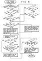
- the CPU 100 executes the index signal check to control the rotation of the motor 6 in response to an output signal from the index sensor 109; the motor control signal check to control the rotation of the motor 6 in response to a motor control signal from the control signal generating circuit 106; the step signal check which will be described later with reference to Fig. 8; and the write-in check to execute the read-write operation to the floppy disk 4 through the magnetic head 16 in response to a write/read signal from the control signal generating circuit 106.
- the CPU 100 first checks whether or not the step signal STP is generated from the control signal generating circuit 106. When it is detected that the step signal STP is not generated in this step, the CPU 100 performs the next processing in the main routine, i.e., the subroutine of the motor control signal check. In addition, when it is detected that the step signal is generated in this step, the CPU 100 checks whether or not data "1" is stored in the memory area Ml in STEP 3. If it is detected that data "1" is stored in the memory area Ml in this STEP 3, the CPU 100 checks whether or not the direction instruction signal DIR from the control signal generating circuit 106 is at "1" level.
- this direction instruction signal DIR is at "1" level in this step
- the CPU 100 returns to the main routine. If it is detected that the direction instruction signal DIR is at "0" level in this step, the CPU 100 stores data, such as to allow the motor 12 to be rotated in the forward direction, in the memory areas MA, MB, MC and MD, respectively, and at the same time it decreases the content of the memory area M2 by one count. Thereafter, the drive signals ⁇ A , ⁇ B , ⁇ C and 4>D corresponding to the contents of the memory areas MA, MB, MC and MD are generated, thereby causing the motor 12 to be rotated by one step in the forward direction to move the maqnetic head 16 by one track in the outer peripheral direction.
- the CPU 100 checks in STEP 5 whether or not an output signal from the detector 22 is at a high level, namely, whether or not the light from the light emitting diode 22A is interrupted by the projecting portion 10A. In the case where it is detected that a low-level signal is generated from this detector 22 in this step, the CPU 100 stops the generation of a track zero signal. When detecting that the direction instruction signal DIR is at "1" level in STEP 4, the CPU 100 inhibits the generation of a track zero signal.
- the CPU 100 checks in STEP 6 whether or not data "1", “0”, “0” and “1” are stored in the memory areas MA, MB, MC and MD, respectively, namely, whether or not the magnetic head is in the track zero position. If an answer in this STEP 6 is "YES”, the CPU 100 clears the contents of the memory areas Ml and M2 and thereafter generates a track zero signal. If the answer is "NO” in this STEP 6, the CPU 100 stops the generation of a track zero signal.
- the CPU 100 checks whether or not data "0" is stored in the memory area M2 in STEP 7. If an answer in this STEP 7 is "YES", i.e., if it is detected that the magnetic head 16 is in the track zero position, it is checked whether or not the direction instruction signal DIR is at "1" level.
- the CPU 100 When it is detected that the direction instruction signal of "0" level is generated, the CPU 100 returns the processing to the main routine, while when it is detected that the direction instruction signal of "1" level is generated, the CPU 100 writes data for allowing the motor 12 to be rotated in the reverse direction into the memory areas MA, MB, MC and MD and at the same time increases the content of the memory area M2 by one count. Thereafter, the drive signals ⁇ A , ⁇ B , ⁇ C and ⁇ D correspondig to the contents of the memory areas MA, MB, MC and MD are generated to move the magnetic head 16 by one track in the inner direction of the floppy disk and then the processing in the previously-described STEP 4 is executed.
- CPU 100 checks whether or not the direction instruction signal DIR is at "1" level. Then, according to the level of the direction instruction signal DIR the CPU 100 writes the data to rotate the motor 12 forwardly or reversely in the memory areas MA, MB, MC and MD as described previously and decreases or increases the content of the memory area M2 by one count, and thereafter the magnetic head 16 is moved by one track in the outer or inner peripheral direction of the floppy disk.
- the magnetic head 16 is moved in the outer peripheral direction in the state in which data "1" is stored in the memory area Ml and the movement of the magnetic head 16 in the inner peripheral direction of the floppy disk is inhibited.
- the CPU 100 when, in STEP 3, it is detected that data "1" is stored in the memory area M1 and that the direction instruction signal DIR of "0" level is generated, the CPU 100 writes the data to rotate the motor 12 in the forward direction in the memory areas MA, MB, MC and MD and at the same time decreases the content of the memory area M2 by one count, and thereafter it supplies the drive signals ⁇ A , ⁇ B , ⁇ C and ⁇ D to the motor driver 112, thereby rotating the motor 12 by one step in the forward direction.
- the magnetic head 16 is moved by one track in the outer peripheral direction of the floppy disk. Similar operations are repeatedly executed so long as the step signal and direction instruction signal of "0" level are generated from the control signal generating circuit 106. Thereafter, when the magnetic head 16 reaches near the outer peripheral limit location and the light from the light emitting diode 22A to the phototransistor 22B is interrupted by the projecting portion 10A, the CPU 100 detects that a high-level signal is generated from the detector 22 in STEP 5 and then executes the processing of STEP 6.
- the CPU 100 In this STEP 6, the CPU 100 generates the drive signals ⁇ A , ⁇ B , ⁇ C and ⁇ D to further rotate the motor 12 in the forward direction until it is detected that data "1", “0”, “0” and “1” are stored in the memory areas MA, MB, MC and MD in this STEP 6. If it is detected that data "1", “Q”, "0” and “1” are respectively stored in the memory areas MA, MB, MC and MD in this STEP 6, the CPU 100 clears the contents of the memory areas Ml and M2 and generates a track zero signal.
- the drive signals ⁇ A , ⁇ B , ⁇ C and ' D corresponding to the data in the memory areas MA, MB, MC and MD are generated, thereby causing the magnetic head 16 to be moved by one track in the inner direction of the floppy disk.
- the processings of STEP 4 and STEP 5 are executed and then the CPU 100 stops the generation of a track zero signal.
- the magentic head 16 is moved by one track at a time in the inner direction of the floppy disk and the content of the memory area M2 is also increased by one count.
- the direction instruction signal DIR is at "1" level
- STEP 4 is executed and STEP 5 is not executed. That is, when the magnetic head 16 is moved in the inner direction of the floppy disk,.a track zero signal will not be generated.
- the same effect is obtained as in the embodiments of Figs. 4 and 5.
- the Q output terminal of the flip-flop 36 may be connected to the input terminal of the AND gate 30 instead of the AND gate 34. It is also possible to connect the direction instruction signal DIR directly to the input terminal of the exclusive OR gate 46 in place of the flip-flop 36 and integrating circuit 44.
- the logic circuit 60 as shown in Fig. 5 may be added to the embodiment shown in Fig. 4.
Landscapes
- Moving Of Head For Track Selection And Changing (AREA)
- Holding Or Fastening Of Disk On Rotational Shaft (AREA)
Applications Claiming Priority (2)
| Application Number | Priority Date | Filing Date | Title |
|---|---|---|---|
| JP58083852A JPS59210574A (ja) | 1983-05-13 | 1983-05-13 | フロツピデイスクドライブ装置 |
| JP83852/83 | 1983-05-13 |
Publications (2)
| Publication Number | Publication Date |
|---|---|
| EP0126371A2 true EP0126371A2 (fr) | 1984-11-28 |
| EP0126371A3 EP0126371A3 (fr) | 1986-11-26 |
Family
ID=13814221
Family Applications (1)
| Application Number | Title | Priority Date | Filing Date |
|---|---|---|---|
| EP84105165A Withdrawn EP0126371A3 (fr) | 1983-05-13 | 1984-05-08 | Appareil de mémoire à disque souple |
Country Status (3)
| Country | Link |
|---|---|
| US (1) | US4599659A (fr) |
| EP (1) | EP0126371A3 (fr) |
| JP (1) | JPS59210574A (fr) |
Cited By (3)
| Publication number | Priority date | Publication date | Assignee | Title |
|---|---|---|---|---|
| US4599659A (en) * | 1983-05-13 | 1986-07-08 | Tokyo Electric Co., Ltd. | Floppy disk drive apparatus |
| US4633346A (en) * | 1984-06-20 | 1986-12-30 | Mitsubishi Denki Kabushiki Kaisha | Magnetic head positioning device for a flexible disk |
| US4686590A (en) * | 1984-06-29 | 1987-08-11 | Kabushiki Kaisha Toshiba | Apparatus for positioning a magnetic head |
Families Citing this family (6)
| Publication number | Priority date | Publication date | Assignee | Title |
|---|---|---|---|---|
| JPH0437346Y2 (fr) * | 1985-12-25 | 1992-09-02 | ||
| JPS639088A (ja) * | 1986-06-30 | 1988-01-14 | Teac Co | デイスク装置 |
| JPS6311403U (fr) * | 1986-07-08 | 1988-01-25 | ||
| JPH07118164B2 (ja) * | 1987-08-31 | 1995-12-18 | 株式会社東芝 | フロッピーディスク装置のシーク制御装置 |
| KR920005212B1 (ko) * | 1990-03-03 | 1992-06-29 | 삼성전자 주식회사 | 플로피 디스크 드라이버의 트랙 제로 감지회로 |
| US6437935B1 (en) * | 1994-11-16 | 2002-08-20 | International Business Machines Corporation | Method and apparatus for a real and positional optimization of a storage disk data zone |
Family Cites Families (8)
| Publication number | Priority date | Publication date | Assignee | Title |
|---|---|---|---|---|
| JPS5730862U (fr) * | 1980-07-29 | 1982-02-18 | ||
| DE3032797A1 (de) * | 1980-08-30 | 1982-04-15 | Basf Ag, 6700 Ludwigshafen | Positioniervorrichtung fuer aufzeichnungs- und/oder abtastorgane in signal-aufzeichnungs-/wiedergabesystemen |
| US4395742A (en) * | 1980-10-15 | 1983-07-26 | Minnesota Mining And Manufacturing Company | Home apparatus |
| US4453188A (en) * | 1981-04-10 | 1984-06-05 | Amlyn Corporation | Disk drive |
| JPS58128059A (ja) * | 1982-01-22 | 1983-07-30 | Canon Electronics Inc | ヘツド位置制御装置 |
| US4547820A (en) * | 1983-01-07 | 1985-10-15 | Tokyo Electric Co., Ltd. | Floppy disk drive apparatus |
| JPS59129971A (ja) * | 1983-01-14 | 1984-07-26 | Tokyo Electric Co Ltd | ディスクドライブ装置 |
| JPS59210574A (ja) * | 1983-05-13 | 1984-11-29 | Tokyo Electric Co Ltd | フロツピデイスクドライブ装置 |
-
1983
- 1983-05-13 JP JP58083852A patent/JPS59210574A/ja active Pending
-
1984
- 1984-05-04 US US06/607,256 patent/US4599659A/en not_active Expired - Fee Related
- 1984-05-08 EP EP84105165A patent/EP0126371A3/fr not_active Withdrawn
Cited By (3)
| Publication number | Priority date | Publication date | Assignee | Title |
|---|---|---|---|---|
| US4599659A (en) * | 1983-05-13 | 1986-07-08 | Tokyo Electric Co., Ltd. | Floppy disk drive apparatus |
| US4633346A (en) * | 1984-06-20 | 1986-12-30 | Mitsubishi Denki Kabushiki Kaisha | Magnetic head positioning device for a flexible disk |
| US4686590A (en) * | 1984-06-29 | 1987-08-11 | Kabushiki Kaisha Toshiba | Apparatus for positioning a magnetic head |
Also Published As
| Publication number | Publication date |
|---|---|
| JPS59210574A (ja) | 1984-11-29 |
| EP0126371A3 (fr) | 1986-11-26 |
| US4599659A (en) | 1986-07-08 |
Similar Documents
| Publication | Publication Date | Title |
|---|---|---|
| US4644419A (en) | Floppy disk unit | |
| US4599659A (en) | Floppy disk drive apparatus | |
| US5010283A (en) | Motor control circuit | |
| US4563712A (en) | Floppy disk drive apparatus | |
| EP0123849B1 (fr) | Moteur pas-à-pas tétraphasé fontionnant en monophase pour mémoire à disque | |
| US4686590A (en) | Apparatus for positioning a magnetic head | |
| US4602301A (en) | Two sided magnetic disk drive apparatus with controlled timing means | |
| EP0356763B1 (fr) | Appareil et méthode d'accès à un milieu à faible consommation d'énergie | |
| US4644426A (en) | Floppy disk drive apparatus | |
| KR910008509B1 (ko) | 데이타 레코딩 장치 | |
| US4479154A (en) | Floppy disk drive with local processor control | |
| US4547820A (en) | Floppy disk drive apparatus | |
| JPH0731410Y2 (ja) | ディスク装置 | |
| EP0595249B1 (fr) | Unité de commande de disques magnétiques capable d'éviter des operations d'écriture erronées | |
| US4754344A (en) | Method and apparatus for formatting magnetic disks with use of host equipment programmed for smaller capacity magnetic disks | |
| US4777545A (en) | Circuit arrangement for inhibiting writing on a magnetic disk during the settling time of a transducer head | |
| KR100205287B1 (ko) | 하드 디스크 드라이브의 액츄에이터 언래칭 감지장치 및 방법 | |
| US4665445A (en) | Floppy disk drive apparatus | |
| KR100482351B1 (ko) | 스핀들모터회전유무감지회로및감지결과출력방법 | |
| US6950262B2 (en) | Flexible disk drive control method capable of preventing a seek error from occurring | |
| KR0156984B1 (ko) | 자기 디스크 구동장치의 헤드 언래칭 인식장치 및 방법 | |
| JPS63160002A (ja) | 光磁気ディスク装置 | |
| US4677358A (en) | Stepping motor drive controlling circuit | |
| KR930001796B1 (ko) | 기억장치의 디스크 기록제어장치 | |
| JP2586010B2 (ja) | 記録装置 |
Legal Events
| Date | Code | Title | Description |
|---|---|---|---|
| PUAI | Public reference made under article 153(3) epc to a published international application that has entered the european phase |
Free format text: ORIGINAL CODE: 0009012 |
|
| 17P | Request for examination filed |
Effective date: 19840508 |
|
| AK | Designated contracting states |
Designated state(s): DE FR GB |
|
| PUAL | Search report despatched |
Free format text: ORIGINAL CODE: 0009013 |
|
| RHK1 | Main classification (correction) |
Ipc: G11B 19/20 |
|
| AK | Designated contracting states |
Kind code of ref document: A3 Designated state(s): DE FR GB |
|
| 17Q | First examination report despatched |
Effective date: 19880530 |
|
| STAA | Information on the status of an ep patent application or granted ep patent |
Free format text: STATUS: THE APPLICATION IS DEEMED TO BE WITHDRAWN |
|
| 18D | Application deemed to be withdrawn |
Effective date: 19881011 |
|
| RIN1 | Information on inventor provided before grant (corrected) |
Inventor name: SAITO, SHUNJI |