EP0126424A2 - Verfahren zur Herstellung von Polycide-Strukturen - Google Patents
Verfahren zur Herstellung von Polycide-Strukturen Download PDFInfo
- Publication number
- EP0126424A2 EP0126424A2 EP84105540A EP84105540A EP0126424A2 EP 0126424 A2 EP0126424 A2 EP 0126424A2 EP 84105540 A EP84105540 A EP 84105540A EP 84105540 A EP84105540 A EP 84105540A EP 0126424 A2 EP0126424 A2 EP 0126424A2
- Authority
- EP
- European Patent Office
- Prior art keywords
- layer
- metal
- mask
- dry etching
- silicon
- Prior art date
- Legal status (The legal status is an assumption and is not a legal conclusion. Google has not performed a legal analysis and makes no representation as to the accuracy of the status listed.)
- Granted
Links
Images

Classifications
-
- H—ELECTRICITY
- H10—SEMICONDUCTOR DEVICES; ELECTRIC SOLID-STATE DEVICES NOT OTHERWISE PROVIDED FOR
- H10D—INORGANIC ELECTRIC SEMICONDUCTOR DEVICES
- H10D30/00—Field-effect transistors [FET]
- H10D30/01—Manufacture or treatment
- H10D30/021—Manufacture or treatment of FETs having insulated gates [IGFET]
- H10D30/0223—Manufacture or treatment of FETs having insulated gates [IGFET] having source and drain regions or source and drain extensions self-aligned to sides of the gate
-
- H—ELECTRICITY
- H10—SEMICONDUCTOR DEVICES; ELECTRIC SOLID-STATE DEVICES NOT OTHERWISE PROVIDED FOR
- H10D—INORGANIC ELECTRIC SEMICONDUCTOR DEVICES
- H10D64/00—Electrodes of devices having potential barriers
- H10D64/01—Manufacture or treatment
- H10D64/013—Manufacture or treatment of electrodes having a conductor capacitively coupled to a semiconductor by an insulator
- H10D64/01302—Manufacture or treatment of electrodes having a conductor capacitively coupled to a semiconductor by an insulator the insulator being formed after the semiconductor body, the semiconductor being silicon
- H10D64/01304—Manufacture or treatment of electrodes having a conductor capacitively coupled to a semiconductor by an insulator the insulator being formed after the semiconductor body, the semiconductor being silicon characterised by the conductor
- H10D64/01306—Manufacture or treatment of electrodes having a conductor capacitively coupled to a semiconductor by an insulator the insulator being formed after the semiconductor body, the semiconductor being silicon characterised by the conductor the conductor comprising a layer of silicon contacting the insulator, e.g. polysilicon
- H10D64/01308—Manufacture or treatment of electrodes having a conductor capacitively coupled to a semiconductor by an insulator the insulator being formed after the semiconductor body, the semiconductor being silicon characterised by the conductor the conductor comprising a layer of silicon contacting the insulator, e.g. polysilicon the conductor further comprising a non-elemental silicon additional conductive layer, e.g. a metal silicide layer formed by the reaction of silicon with an implanted metal
- H10D64/01312—Manufacture or treatment of electrodes having a conductor capacitively coupled to a semiconductor by an insulator the insulator being formed after the semiconductor body, the semiconductor being silicon characterised by the conductor the conductor comprising a layer of silicon contacting the insulator, e.g. polysilicon the conductor further comprising a non-elemental silicon additional conductive layer, e.g. a metal silicide layer formed by the reaction of silicon with an implanted metal the additional layer comprising a metal or metal silicide formed by deposition, i.e. without a silicidation reaction, e.g. sputter deposition
-
- H—ELECTRICITY
- H10—SEMICONDUCTOR DEVICES; ELECTRIC SOLID-STATE DEVICES NOT OTHERWISE PROVIDED FOR
- H10D—INORGANIC ELECTRIC SEMICONDUCTOR DEVICES
- H10D64/00—Electrodes of devices having potential barriers
- H10D64/01—Manufacture or treatment
- H10D64/013—Manufacture or treatment of electrodes having a conductor capacitively coupled to a semiconductor by an insulator
- H10D64/01302—Manufacture or treatment of electrodes having a conductor capacitively coupled to a semiconductor by an insulator the insulator being formed after the semiconductor body, the semiconductor being silicon
- H10D64/01304—Manufacture or treatment of electrodes having a conductor capacitively coupled to a semiconductor by an insulator the insulator being formed after the semiconductor body, the semiconductor being silicon characterised by the conductor
- H10D64/01326—Aspects related to lithography, isolation or planarisation of the conductor
-
- H—ELECTRICITY
- H10—SEMICONDUCTOR DEVICES; ELECTRIC SOLID-STATE DEVICES NOT OTHERWISE PROVIDED FOR
- H10P—GENERIC PROCESSES OR APPARATUS FOR THE MANUFACTURE OR TREATMENT OF DEVICES COVERED BY CLASS H10
- H10P50/00—Etching of wafers, substrates or parts of devices
- H10P50/20—Dry etching; Plasma etching; Reactive-ion etching
- H10P50/26—Dry etching; Plasma etching; Reactive-ion etching of conductive or resistive materials
- H10P50/264—Dry etching; Plasma etching; Reactive-ion etching of conductive or resistive materials by chemical means
- H10P50/266—Dry etching; Plasma etching; Reactive-ion etching of conductive or resistive materials by chemical means by vapour etching only
- H10P50/267—Dry etching; Plasma etching; Reactive-ion etching of conductive or resistive materials by chemical means by vapour etching only using plasmas
- H10P50/268—Dry etching; Plasma etching; Reactive-ion etching of conductive or resistive materials by chemical means by vapour etching only using plasmas of silicon-containing layers
-
- H—ELECTRICITY
- H10—SEMICONDUCTOR DEVICES; ELECTRIC SOLID-STATE DEVICES NOT OTHERWISE PROVIDED FOR
- H10P—GENERIC PROCESSES OR APPARATUS FOR THE MANUFACTURE OR TREATMENT OF DEVICES COVERED BY CLASS H10
- H10P50/00—Etching of wafers, substrates or parts of devices
- H10P50/60—Wet etching
- H10P50/66—Wet etching of conductive or resistive materials
- H10P50/663—Wet etching of conductive or resistive materials by chemical means only
- H10P50/667—Wet etching of conductive or resistive materials by chemical means only by liquid etching only
-
- H—ELECTRICITY
- H10—SEMICONDUCTOR DEVICES; ELECTRIC SOLID-STATE DEVICES NOT OTHERWISE PROVIDED FOR
- H10P—GENERIC PROCESSES OR APPARATUS FOR THE MANUFACTURE OR TREATMENT OF DEVICES COVERED BY CLASS H10
- H10P76/00—Manufacture or treatment of masks on semiconductor bodies, e.g. by lithography or photolithography
- H10P76/20—Manufacture or treatment of masks on semiconductor bodies, e.g. by lithography or photolithography of masks comprising organic materials
- H10P76/202—Manufacture or treatment of masks on semiconductor bodies, e.g. by lithography or photolithography of masks comprising organic materials for lift-off processes
-
- H—ELECTRICITY
- H10—SEMICONDUCTOR DEVICES; ELECTRIC SOLID-STATE DEVICES NOT OTHERWISE PROVIDED FOR
- H10W—GENERIC PACKAGES, INTERCONNECTIONS, CONNECTORS OR OTHER CONSTRUCTIONAL DETAILS OF DEVICES COVERED BY CLASS H10
- H10W20/00—Interconnections in chips, wafers or substrates
- H10W20/01—Manufacture or treatment
- H10W20/031—Manufacture or treatment of conductive parts of the interconnections
- H10W20/056—Manufacture or treatment of conductive parts of the interconnections by filling conductive material into holes, grooves or trenches
- H10W20/058—Manufacture or treatment of conductive parts of the interconnections by filling conductive material into holes, grooves or trenches by depositing on sacrificial masks, e.g. using lift-off
-
- H—ELECTRICITY
- H10—SEMICONDUCTOR DEVICES; ELECTRIC SOLID-STATE DEVICES NOT OTHERWISE PROVIDED FOR
- H10W—GENERIC PACKAGES, INTERCONNECTIONS, CONNECTORS OR OTHER CONSTRUCTIONAL DETAILS OF DEVICES COVERED BY CLASS H10
- H10W20/00—Interconnections in chips, wafers or substrates
- H10W20/01—Manufacture or treatment
- H10W20/031—Manufacture or treatment of conductive parts of the interconnections
- H10W20/064—Manufacture or treatment of conductive parts of the interconnections by modifying the conductivity of conductive parts, e.g. by alloying
- H10W20/066—Manufacture or treatment of conductive parts of the interconnections by modifying the conductivity of conductive parts, e.g. by alloying by forming silicides of refractory metals
-
- Y—GENERAL TAGGING OF NEW TECHNOLOGICAL DEVELOPMENTS; GENERAL TAGGING OF CROSS-SECTIONAL TECHNOLOGIES SPANNING OVER SEVERAL SECTIONS OF THE IPC; TECHNICAL SUBJECTS COVERED BY FORMER USPC CROSS-REFERENCE ART COLLECTIONS [XRACs] AND DIGESTS
- Y10—TECHNICAL SUBJECTS COVERED BY FORMER USPC
- Y10S—TECHNICAL SUBJECTS COVERED BY FORMER USPC CROSS-REFERENCE ART COLLECTIONS [XRACs] AND DIGESTS
- Y10S148/00—Metal treatment
- Y10S148/084—Ion implantation of compound devices
-
- Y—GENERAL TAGGING OF NEW TECHNOLOGICAL DEVELOPMENTS; GENERAL TAGGING OF CROSS-SECTIONAL TECHNOLOGIES SPANNING OVER SEVERAL SECTIONS OF THE IPC; TECHNICAL SUBJECTS COVERED BY FORMER USPC CROSS-REFERENCE ART COLLECTIONS [XRACs] AND DIGESTS
- Y10—TECHNICAL SUBJECTS COVERED BY FORMER USPC
- Y10S—TECHNICAL SUBJECTS COVERED BY FORMER USPC CROSS-REFERENCE ART COLLECTIONS [XRACs] AND DIGESTS
- Y10S438/00—Semiconductor device manufacturing: process
- Y10S438/942—Masking
- Y10S438/948—Radiation resist
- Y10S438/951—Lift-off
Definitions
- the invention relates to a process for making a polycide structure where on an insulating layer deposited on a substrate a polysilicon layer, and on top of it a silicide layer and a dry etching metal mask are formed and at least the exposed regions of the polysilicon layer are dry etched, and to an application of said process.
- Polycrystalline silicon hereafter referred to as polysilicon
- polysilicon has been used in semiconductor technology because of its high temperature stability and its ability to provide a stable insulating layer by self- passivation.
- Doped polysilicon has been used as an electrode and interconnecting line material especially for applications requiring conductive materials that are self-passivating.
- the scaling down of device dimensions causes the resistance of polysilicon lines to increase to levels which seriously impair device performance.
- metal silicides may be used with or without doped polysilicon layers for a variety of electrode and wiring interconnection applications.
- silicides may also be self-passivating, as a layer of silicon dioxide forms on the free or open surfaces of the silicide when exposed to an oxidizing ambient.
- a composite conducting line of doped polysilicon and metal silicide is referred to as polycide.
- Polycide structures yield the combined advantage of high conductivity and reduced parasitic capacitance.
- a method for making silicides is taught in U.S. Patent 4,128,670, entitled, "Fabrication Method for Integrated Circuits with Polysilicon Lines Having Low Sheet Resistance,” issued on December 5, 1978 to Fritz H. Gaensslen and assigned to the present assignee.
- U.S. Patent 4,329,706 entitled, "Doped Polysilicon Silicide Semiconductor Integrated Circuit Interconnections", issued on May 11, 1982 to B.L. Crowder et al discloses the use of a polycide material for interconnecting members.
- the silicide layer is formed or deposited by co-evaporation, sputtering or chemical vacuum deposition so that in the process either the metal combines with the polysilicon to form the silicide or in the alternative the silicide is made up of a mixture of co-deposited metal and silicon.
- the materials are etched using conventional etching techniques.
- Levin- stein et al discloses a method for making cobalt disilicide electrode metallization contacts to underlying silicon. It includes depositing and then sintering a layer of cobalt on a patterned semiconductor wafer having exposed polysilicon or monocrystalline silicon portions. The cobalt reacts with the exposed silicon portions and forms cobalt monosilicide (CoSi) or di-cobalt silicide (Co 2 Si) or a mixture of both. The unreacted cobalt is selectively removed, as by selective etching in a suitable acid bath. This is then followed by a heat treatment to convert the cobalt compound(s) into cobalt disilicide (CoSi 2 ). A layer of polysilicon is deposited over the cobalt disilicide, followed by gettering, a deposition of aluminum and standard etch-patterning of the aluminum and polysilicon layers.
- the European patent application 0096773 discloses a method of making a silicide structure which includes the steps of depositing a metal layer directly onto a thin insulating layer of silicon dioxide formed on a semiconductor substrate, co-depositing metal and silicon onto the metal layer and then depositing silicon onto the co-deposited metal-silicon layer. Upon annealing this structure, a metal silicide forms down to the thin silicon dioxide layer.
- the inventive process has all the advantages of the known methods to form polycide structures. It extends the developments in this area of technology and has further advantages and flexibilities. Using the inventive process all elements in the polycide structure have a uniform line width. The inventive process is advantageously compatible with evaporative lift-off techniques.
- the silicide layer is either produced by co-depositing a silicide forming metal and silicon followed by an anneal step, or by depositing a silicide laver by - for example - chemical vapor deposition. Due to the heat to which the structure is exposed during the anneal step in the first case a diffusion layer is required between the metal mask and the underlying layers in order to prevent a diffusion of the mask forming metal into these layers. In the second case a diffusion barrier layer can be omitted, because no anneal step is necessary.
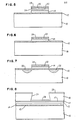
- a semiconductor substrate 10 which may be N-type or P-type monocrystalline silicon depending on the planned uses of the resulting structure.
- substrate 10 On substrate 10, there is an insulating layer 12 which in the case of a silicon substrate may be a layer of silicon dioxide (Si0 2 ) which may be grown through the thermal oxidation of silicon. If the resulting polycide structure is to be used as a gate electrode then this layer 12 will form the gate dielectric and will typically have a thickness in the range of 200 to 500 A°.
- a blanket layer 14 of doped polysilicon is deposited on layer 12. This layer of polysilicon can be of any suitable thickness but is typically in the range of 1,000 to 4,000 A°. In Fig.
- a photoresist layer 16 with an opening 18 formed therein, by known techniques, to expose a predetermined portion of the surface 20 of the polysilicon layer 14.
- the definition of opening 18 and the photoresist slope angles are designed to be compatible with lift-off techniques.
- Fig. 3 there is shown the structure after the sequential deposition through the opening 18 and over the photoresist mask of several layers.
- a metal silicide layer 22 On top of exposed portion of polysilicon layer 14 is a metal silicide layer 22 as indicated in Fig. 3.
- the thickness of layer 22 is in general dependant on the thickness of polysilicon layer 14. Typically, the thickness of silicide layer 22 should be comparable to the thickness of layer 16 which is typically in the range of 1,000 to 4,000 A°.
- the metal of the metal silicide layer 22 is preferably a refractory metal such as tungsten, titanium, niobium, molybdenum, tantalum, iridium or rhodium.
- the metal silicide layer 22 can be deposited by any suitable technique, such as the co-evaporation of the metal and silicon while heating the respective targets of metal and silicon with E-Beams. This forms first a composite metal-silicon layer which during a subsequent annealing step turns into the corresponding metal silicide layer. Then, pure silicon layer 24 is deposited over layer 22 to serve as a capping layer to improve the subsequent oxidation behavior of the overall polycide structure.
- a thin diffusion barrier layer 26 such as a layer of tungsten (W) is deposited again through evaporation over silicon layer 24.
- the typical thickness of this layer is in the range between 250 and 500 A°.
- a tungsten layer 26 will not react with the silicon capping layer 24 below the temperature range of 650° C to 700° C.
- This masking layer is made of a refractory metal that does not form a volatile halide in a dry etching environment and can be removed through wet etching with chemicals that do not etch the other materials present in the structure without contaminating the structure. Furthermore, this masking material must be compatible with the diffusion barrier layer material so that it does not chemically react with that material.
- metal mask 28 may be formed, for example, by the evaporation of cobalt (Co) over tungsten (W) layer 26. This is followed by removal through a conventional lift-off step of the photoresist layer 16 with all the excess materials deposited on it. This results in a structure as shown in Fig. 4. Then there is a need for the structure to go through low temperature reaction annealing at a temperature preferably in the range of 500° to 600° C for a reaction of the metal and silicon in the composite metal-silicon layer to form the corresponding metal silicide.
- the W will not react with Si, and Co will be prevented from diffusing into Si by the W layer that separates the two.
- the structure is then subjected to dry etching, preferably a RIE step, to remove the polysilicon layer 14 from all but the gate region as defined by metal mask 28 and to produce vertical gate electrode sidewalls.
- a RIE can be performed using an environment such as CF 4 + 0 2 .
- CoF 2 cobalt fluoride
- etching will stop when the unmasked portion of polysilicon layer 14 is entirely removed, that is, when it reaches the surface of Si0 2 layer 12, as shown in Fig. 5.
- the metal mask is then removed using a conventional chemical cleaning process. For example a mixture of HCl, H 2 0 2 and H 2 0 will remove a Co, Fe, Ni or Mn mask from a polycide structure at 60-70° C in about 5 minutes.
- the tungsten (W) layer 26 is also removed using a conventional wet etching step such as, for example, with a mixture having of NH 4 0H, H 2 0 2 and H 2 0 at 60-70° C for about 5 minutes to produce the structure shown in Fig. 6.
- a conventional ion implantation step and the gate electrode as a implantation mask self-aligned source and drain regions 30 and 32 may be formed in the substrate. This results in the structure shown in Fig. 7.
- a homogenization anneal at a temperature range of 950° to 1100 0 C for the further homogenization of the silicide structure.
- Fig. 8 there is shown an alternative method for practicing the invention, wherein first an insulating layer 12 is formed on a substrate 10.
- a polysilicon layer 14 is deposited on the insulating layer 12 and a metal silicide layer 15 is deposited through chemical vapor deposition on the polysilicon layer 14.
- a silicon capping layer 17 is deposited over the metal silicide layer 15 and a photoresist mask 19 is formed over silicon layer 17.
- This photoresist mask is made to be compatible with lift-off techniques.
- a refractory metal layer 28 selected from a group of metals consisting of cobalt, iron, nickel and manganese, is deposited through opening 21 onto exposed portion of silicon layer 17.
- the photoresist mask 19 and the excess refractory metal on it are lifted off and the structure is then dry etched, using for example a RIE step, and using metal layer 28 as an etching mask. This results in a polycide structure on insulating layer 12.
- the mask is then removed with a chemical etch as described above in the discussions of Fig. 5.
Landscapes
- Electrodes Of Semiconductors (AREA)
Applications Claiming Priority (2)
| Application Number | Priority Date | Filing Date | Title |
|---|---|---|---|
| US06/497,372 US4470189A (en) | 1983-05-23 | 1983-05-23 | Process for making polycide structures |
| US497372 | 1983-05-23 |
Publications (3)
| Publication Number | Publication Date |
|---|---|
| EP0126424A2 true EP0126424A2 (de) | 1984-11-28 |
| EP0126424A3 EP0126424A3 (en) | 1988-01-13 |
| EP0126424B1 EP0126424B1 (de) | 1990-11-28 |
Family
ID=23976595
Family Applications (1)
| Application Number | Title | Priority Date | Filing Date |
|---|---|---|---|
| EP84105540A Expired EP0126424B1 (de) | 1983-05-23 | 1984-05-16 | Verfahren zur Herstellung von Polycide-Strukturen |
Country Status (4)
| Country | Link |
|---|---|
| US (1) | US4470189A (de) |
| EP (1) | EP0126424B1 (de) |
| JP (1) | JPS59217328A (de) |
| DE (1) | DE3483659D1 (de) |
Cited By (1)
| Publication number | Priority date | Publication date | Assignee | Title |
|---|---|---|---|---|
| FR2664429A1 (fr) * | 1990-07-02 | 1992-01-10 | Samsung Electronics Co Ltd | Procede de realisation d'une configuration d'interconnexion en tungstene. |
Families Citing this family (35)
| Publication number | Priority date | Publication date | Assignee | Title |
|---|---|---|---|---|
| US4546535A (en) * | 1983-12-12 | 1985-10-15 | International Business Machines Corporation | Method of making submicron FET structure |
| US4636834A (en) * | 1983-12-12 | 1987-01-13 | International Business Machines Corporation | Submicron FET structure and method of making |
| US4551906A (en) * | 1983-12-12 | 1985-11-12 | International Business Machines Corporation | Method for making self-aligned lateral bipolar transistors |
| FR2571177B1 (fr) * | 1984-10-02 | 1987-02-27 | Thomson Csf | Procede de realisation de grilles en siliciure ou en silicium pour circuit integre comportant des elements du type grille - isolant - semi-conducteur |
| US4612258A (en) * | 1984-12-21 | 1986-09-16 | Zilog, Inc. | Method for thermally oxidizing polycide substrates in a dry oxygen environment and semiconductor circuit structures produced thereby |
| US4663191A (en) * | 1985-10-25 | 1987-05-05 | International Business Machines Corporation | Salicide process for forming low sheet resistance doped silicon junctions |
| US4709655A (en) * | 1985-12-03 | 1987-12-01 | Varian Associates, Inc. | Chemical vapor deposition apparatus |
| US4796562A (en) * | 1985-12-03 | 1989-01-10 | Varian Associates, Inc. | Rapid thermal cvd apparatus |
| JPS6362356A (ja) * | 1986-09-03 | 1988-03-18 | Mitsubishi Electric Corp | 半導体装置 |
| GB8710359D0 (en) * | 1987-05-01 | 1987-06-03 | Inmos Ltd | Semiconductor element |
| US4974056A (en) * | 1987-05-22 | 1990-11-27 | International Business Machines Corporation | Stacked metal silicide gate structure with barrier |
| JPH01120818A (ja) * | 1987-09-23 | 1989-05-12 | Siemens Ag | 低伝達抵抗オーム接触の形成方法 |
| JP2624797B2 (ja) * | 1988-09-20 | 1997-06-25 | 株式会社日立製作所 | アクティブマトリクス基板の製造方法 |
| US4978637A (en) * | 1989-05-31 | 1990-12-18 | Sgs-Thomson Microelectronics, Inc. | Local interconnect process for integrated circuits |
| KR920015622A (ko) * | 1991-01-31 | 1992-08-27 | 원본미기재 | 집적 회로의 제조방법 |
| US5334545A (en) * | 1993-02-01 | 1994-08-02 | Allied Signal Inc. | Process for forming self-aligning cobalt silicide T-gates of silicon MOS devices |
| US6284584B1 (en) | 1993-12-17 | 2001-09-04 | Stmicroelectronics, Inc. | Method of masking for periphery salicidation of active regions |
| US6107194A (en) * | 1993-12-17 | 2000-08-22 | Stmicroelectronics, Inc. | Method of fabricating an integrated circuit |
| JP3045946B2 (ja) * | 1994-05-09 | 2000-05-29 | インターナショナル・ビジネス・マシーンズ・コーポレイション | 半導体デバイスの製造方法 |
| US5847463A (en) * | 1997-08-22 | 1998-12-08 | Micron Technology, Inc. | Local interconnect comprising titanium nitride barrier layer |
| JP3209164B2 (ja) * | 1997-10-07 | 2001-09-17 | 日本電気株式会社 | 半導体装置の製造方法 |
| KR100269328B1 (ko) * | 1997-12-31 | 2000-10-16 | 윤종용 | 원자층 증착 공정을 이용하는 도전층 형성방법 |
| US6235630B1 (en) * | 1998-08-19 | 2001-05-22 | Micron Technology, Inc. | Silicide pattern structures and methods of fabricating the same |
| US6214713B1 (en) * | 1998-10-19 | 2001-04-10 | Promos Technology, Inc. | Two step cap nitride deposition for forming gate electrodes |
| US6077750A (en) * | 1998-10-27 | 2000-06-20 | Lg Semicon Co., Ltd. | Method for forming epitaxial Co self-align silicide for semiconductor device |
| KR100505449B1 (ko) * | 1998-12-24 | 2005-10-14 | 주식회사 하이닉스반도체 | 반도체 소자의 폴리사이드 게이트 전극 형성방법 |
| US6251777B1 (en) | 1999-03-05 | 2001-06-26 | Taiwan Semiconductor Manufacturing Company | Thermal annealing method for forming metal silicide layer |
| US6475911B1 (en) * | 2000-08-16 | 2002-11-05 | Micron Technology, Inc. | Method of forming noble metal pattern |
| DE10121240C1 (de) * | 2001-04-30 | 2002-06-27 | Infineon Technologies Ag | Verfahren zur Herstellung für eine integrierte Schaltung, insbesondere eine Anti-Fuse, und entsprechende integrierte Schaltung |
| US7049245B2 (en) * | 2003-09-12 | 2006-05-23 | Promos Technologies, Inc. | Two-step GC etch for GC profile and process window improvement |
| US7678704B2 (en) * | 2005-12-13 | 2010-03-16 | Infineon Technologies Ag | Method of making a contact in a semiconductor device |
| US20070161246A1 (en) * | 2006-01-10 | 2007-07-12 | Texas Instruments Incorporated | Process For Selectively Removing Dielectric Material in the Presence of Metal Silicide |
| TW200833871A (en) * | 2006-11-17 | 2008-08-16 | Sachem Inc | Selective metal wet etch composition and process |
| JP7036001B2 (ja) * | 2018-12-28 | 2022-03-15 | 三菱電機株式会社 | 半導体装置の製造方法 |
| CN110661170B (zh) * | 2019-08-13 | 2021-01-08 | 深圳市矽赫科技有限公司 | 一种用于制造半导体器件隔离结构的方法及其半导体器件 |
Family Cites Families (11)
| Publication number | Priority date | Publication date | Assignee | Title |
|---|---|---|---|---|
| US4180596A (en) * | 1977-06-30 | 1979-12-25 | International Business Machines Corporation | Method for providing a metal silicide layer on a substrate |
| US4128670A (en) * | 1977-11-11 | 1978-12-05 | International Business Machines Corporation | Fabrication method for integrated circuits with polysilicon lines having low sheet resistance |
| US4329706A (en) * | 1979-03-01 | 1982-05-11 | International Business Machines Corporation | Doped polysilicon silicide semiconductor integrated circuit interconnections |
| DE3045922A1 (de) * | 1980-12-05 | 1982-07-08 | Siemens AG, 1000 Berlin und 8000 München | Verfahren zum herstellen von strukturen von aus siliziden oder aus silizid-polysilizium bestehenden schichten durch reaktives sputteraetzen |
| US4352716A (en) * | 1980-12-24 | 1982-10-05 | International Business Machines Corporation | Dry etching of copper patterns |
| US4362597A (en) * | 1981-01-19 | 1982-12-07 | Bell Telephone Laboratories, Incorporated | Method of fabricating high-conductivity silicide-on-polysilicon structures for MOS devices |
| US4389257A (en) * | 1981-07-30 | 1983-06-21 | International Business Machines Corporation | Fabrication method for high conductivity, void-free polysilicon-silicide integrated circuit electrodes |
| US4378628A (en) * | 1981-08-27 | 1983-04-05 | Bell Telephone Laboratories, Incorporated | Cobalt silicide metallization for semiconductor integrated circuits |
| US4398341A (en) * | 1981-09-21 | 1983-08-16 | International Business Machines Corp. | Method of fabricating a highly conductive structure |
| US4414057A (en) * | 1982-12-03 | 1983-11-08 | Inmos Corporation | Anisotropic silicide etching process |
| US4411734A (en) * | 1982-12-09 | 1983-10-25 | Rca Corporation | Etching of tantalum silicide/doped polysilicon structures |
-
1983
- 1983-05-23 US US06/497,372 patent/US4470189A/en not_active Expired - Lifetime
-
1984
- 1984-01-18 JP JP59005865A patent/JPS59217328A/ja active Granted
- 1984-05-16 DE DE8484105540T patent/DE3483659D1/de not_active Expired - Lifetime
- 1984-05-16 EP EP84105540A patent/EP0126424B1/de not_active Expired
Cited By (1)
| Publication number | Priority date | Publication date | Assignee | Title |
|---|---|---|---|---|
| FR2664429A1 (fr) * | 1990-07-02 | 1992-01-10 | Samsung Electronics Co Ltd | Procede de realisation d'une configuration d'interconnexion en tungstene. |
Also Published As
| Publication number | Publication date |
|---|---|
| JPH0412612B2 (de) | 1992-03-05 |
| JPS59217328A (ja) | 1984-12-07 |
| EP0126424B1 (de) | 1990-11-28 |
| US4470189A (en) | 1984-09-11 |
| DE3483659D1 (de) | 1991-01-10 |
| EP0126424A3 (en) | 1988-01-13 |
Similar Documents
| Publication | Publication Date | Title |
|---|---|---|
| EP0126424B1 (de) | Verfahren zur Herstellung von Polycide-Strukturen | |
| EP0071029B1 (de) | Verfahren zum Herstellen selbstpassivierter zusammengesetzter leitender Silizium-Silizid-Elektroden | |
| EP0219827B1 (de) | Herstellungsverfahren von Metallsilicidschichten von niedrigem Widerstand auf Halbleitersubstraten | |
| KR100530401B1 (ko) | 저저항 게이트 전극을 구비하는 반도체 장치 | |
| US4735680A (en) | Method for the self-aligned silicide formation in IC fabrication | |
| US4332839A (en) | Method for making integrated semiconductor circuit structure with formation of Ti or Ta silicide | |
| EP0068154B1 (de) | Integrierte Schaltung mit einem Halbleitersubstrat mit Isolationszonen und elektrisch leitenden Zonen | |
| US5801444A (en) | Multilevel electronic structures containing copper layer and copper-semiconductor layers | |
| JPH0613403A (ja) | Mos集積回路上の自己整列珪化コバルト | |
| JPH04211134A (ja) | 集積回路及びその製造方法 | |
| US20050130380A1 (en) | Semiconductor device structures including metal silicide interconnects and dielectric layers at substantially the same fabrication level | |
| WO1994000878A1 (en) | Methods of forming a local interconnect and a high resistor polysilicon load | |
| EP0404372B1 (de) | Verfahren zur Herstellung von polykristallinen Siliziumkontakten | |
| EP0472804B1 (de) | Kupfer-Germanium Verbindungen, die bei Niedrigtemperatur hergestellt werden können | |
| US5322815A (en) | Method for producing semiconductor device with multilayer leads | |
| USRE32207E (en) | Method for making integrated semiconductor circuit structure with formation of Ti or Ta silicide | |
| JP3061891B2 (ja) | 半導体装置の製造方法 | |
| US6291890B1 (en) | Semiconductor device having a silicide structure | |
| US5698468A (en) | Silicidation process with etch stop | |
| KR100206683B1 (ko) | 실리사이드 영역상의 보호 장벽 형성 방법 | |
| US5946595A (en) | Method of forming a local interconnect between electronic devices on a semiconductor substrate | |
| US5329161A (en) | Molybdenum boride barrier layers between aluminum and silicon at contact points in semiconductor devices | |
| KR100223736B1 (ko) | 반도체 소자 제조 방법 | |
| US6063692A (en) | Oxidation barrier composed of a silicide alloy for a thin film and method of construction | |
| JPH1064898A (ja) | 半導体装置の製造方法 |
Legal Events
| Date | Code | Title | Description |
|---|---|---|---|
| PUAI | Public reference made under article 153(3) epc to a published international application that has entered the european phase |
Free format text: ORIGINAL CODE: 0009012 |
|
| AK | Designated contracting states |
Designated state(s): DE FR GB |
|
| 17P | Request for examination filed |
Effective date: 19841123 |
|
| PUAL | Search report despatched |
Free format text: ORIGINAL CODE: 0009013 |
|
| AK | Designated contracting states |
Kind code of ref document: A3 Designated state(s): DE FR GB |
|
| 17Q | First examination report despatched |
Effective date: 19890802 |
|
| GRAA | (expected) grant |
Free format text: ORIGINAL CODE: 0009210 |
|
| AK | Designated contracting states |
Kind code of ref document: B1 Designated state(s): DE FR GB |
|
| REF | Corresponds to: |
Ref document number: 3483659 Country of ref document: DE Date of ref document: 19910110 |
|
| ET | Fr: translation filed | ||
| PLBE | No opposition filed within time limit |
Free format text: ORIGINAL CODE: 0009261 |
|
| STAA | Information on the status of an ep patent application or granted ep patent |
Free format text: STATUS: NO OPPOSITION FILED WITHIN TIME LIMIT |
|
| 26N | No opposition filed | ||
| PGFP | Annual fee paid to national office [announced via postgrant information from national office to epo] |
Ref country code: GB Payment date: 19950413 Year of fee payment: 12 |
|
| PGFP | Annual fee paid to national office [announced via postgrant information from national office to epo] |
Ref country code: FR Payment date: 19960507 Year of fee payment: 13 |
|
| PG25 | Lapsed in a contracting state [announced via postgrant information from national office to epo] |
Ref country code: GB Effective date: 19960516 |
|
| GBPC | Gb: european patent ceased through non-payment of renewal fee |
Effective date: 19960516 |
|
| PG25 | Lapsed in a contracting state [announced via postgrant information from national office to epo] |
Ref country code: FR Free format text: LAPSE BECAUSE OF NON-PAYMENT OF DUE FEES Effective date: 19980130 |
|
| REG | Reference to a national code |
Ref country code: FR Ref legal event code: ST |
|
| PGFP | Annual fee paid to national office [announced via postgrant information from national office to epo] |
Ref country code: DE Payment date: 19980522 Year of fee payment: 15 |
|
| PG25 | Lapsed in a contracting state [announced via postgrant information from national office to epo] |
Ref country code: DE Free format text: LAPSE BECAUSE OF NON-PAYMENT OF DUE FEES Effective date: 20000301 |