EP0127725A1 - Procédé pour la fabrication d'un dispositif semi-conducteur comportant des régions faiblement dotées - Google Patents
Procédé pour la fabrication d'un dispositif semi-conducteur comportant des régions faiblement dotées Download PDFInfo
- Publication number
- EP0127725A1 EP0127725A1 EP84100874A EP84100874A EP0127725A1 EP 0127725 A1 EP0127725 A1 EP 0127725A1 EP 84100874 A EP84100874 A EP 84100874A EP 84100874 A EP84100874 A EP 84100874A EP 0127725 A1 EP0127725 A1 EP 0127725A1
- Authority
- EP
- European Patent Office
- Prior art keywords
- film
- crystalline silicon
- impurity
- films
- residual
- Prior art date
- Legal status (The legal status is an assumption and is not a legal conclusion. Google has not performed a legal analysis and makes no representation as to the accuracy of the status listed.)
- Granted
Links
Images


Classifications
-
- H—ELECTRICITY
- H10—SEMICONDUCTOR DEVICES; ELECTRIC SOLID-STATE DEVICES NOT OTHERWISE PROVIDED FOR
- H10D—INORGANIC ELECTRIC SEMICONDUCTOR DEVICES
- H10D64/00—Electrodes of devices having potential barriers
- H10D64/01—Manufacture or treatment
- H10D64/015—Manufacture or treatment removing at least parts of gate spacers, e.g. disposable spacers
-
- H—ELECTRICITY
- H10—SEMICONDUCTOR DEVICES; ELECTRIC SOLID-STATE DEVICES NOT OTHERWISE PROVIDED FOR
- H10D—INORGANIC ELECTRIC SEMICONDUCTOR DEVICES
- H10D30/00—Field-effect transistors [FET]
- H10D30/01—Manufacture or treatment
- H10D30/021—Manufacture or treatment of FETs having insulated gates [IGFET]
- H10D30/0223—Manufacture or treatment of FETs having insulated gates [IGFET] having source and drain regions or source and drain extensions self-aligned to sides of the gate
- H10D30/0227—Manufacture or treatment of FETs having insulated gates [IGFET] having source and drain regions or source and drain extensions self-aligned to sides of the gate having both lightly-doped source and drain extensions and source and drain regions self-aligned to the sides of the gate, e.g. lightly-doped drain [LDD] MOSFET or double-diffused drain [DDD] MOSFET
-
- H—ELECTRICITY
- H10—SEMICONDUCTOR DEVICES; ELECTRIC SOLID-STATE DEVICES NOT OTHERWISE PROVIDED FOR
- H10D—INORGANIC ELECTRIC SEMICONDUCTOR DEVICES
- H10D30/00—Field-effect transistors [FET]
- H10D30/60—Insulated-gate field-effect transistors [IGFET]
-
- H—ELECTRICITY
- H10—SEMICONDUCTOR DEVICES; ELECTRIC SOLID-STATE DEVICES NOT OTHERWISE PROVIDED FOR
- H10P—GENERIC PROCESSES OR APPARATUS FOR THE MANUFACTURE OR TREATMENT OF DEVICES COVERED BY CLASS H10
- H10P76/00—Manufacture or treatment of masks on semiconductor bodies, e.g. by lithography or photolithography
- H10P76/40—Manufacture or treatment of masks on semiconductor bodies, e.g. by lithography or photolithography of masks comprising inorganic materials
- H10P76/408—Manufacture or treatment of masks on semiconductor bodies, e.g. by lithography or photolithography of masks comprising inorganic materials characterised by their sizes, orientations, dispositions, behaviours or shapes
- H10P76/4085—Manufacture or treatment of masks on semiconductor bodies, e.g. by lithography or photolithography of masks comprising inorganic materials characterised by their sizes, orientations, dispositions, behaviours or shapes characterised by the processes involved to create the masks
Definitions
- the present invention relates to a method for manufacturing a semiconductor device and, more particularly to a method for manufacturing a MOS semiconductor device having an LDD (lightly doped drain) structure.
- LDD lightly doped drain
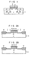
- a source region 2 and a drain region 3 are formed in a surface region of a p-type silicon substrate 1.
- the source region 2 comprises an n -type region 2a of a low impurity concentration and an n +- type region 2b of a high impurity concentration.
- the drain region 3 comprises an n - -type region 3a of a low impurity concentration and an n + - type region 3b of a high impurity concentration.
- the impurity concentrations of the n- -typ e regions 2 a and 3 a are set to be 10 16 to 10 18 cm -3
- the impurity concentrations of the n+- type regions 2b and 3b are set to be about 10 19 to 10 21 cm -3
- a gate electrode 5 is formed on a channel region between the n -type regions 2a and 3a through a gate oxide film 4. In this manner, the n -type region 3a is formed in that portion of the drain region 3 which is located on the side of the channel region, so that a high electric field in the channel region can be weakened. The above problem can thus be solved.
- a thermal oxide film 13 serving as a gate oxide film is formed on a prospective element formation surface surrounded by the field oxide film 12.
- a polycrystalline silicon film, a silicon nitride film and a CVD oxide film are sequentially formed and patterned to form a polycrystalline silicon film pattern 14, a silicon nitride film pattern 15 and a CVD oxide film pattern 16 which are larger in size than a final gate electrode.
- an n-type impurity is ion-implanted in the silicon substrate 11 at a high dose using these patterns as a mask (Fig. 2A).
- an n-type impurity is ion-implanted at a low dose in the silicon substrate 11 using the gate electrode 17 as a mask (Fig. 2C).
- annealing is performed to activate ion-implanted layers formed by performing the above ion implantation technique twice to form a source region 18 and a drain region 19.
- the source region 18 comprises an n -type region 18a and an adjoining n +- type region 18b
- the drain region 19 comprises an n -type region 19a and an adjoining n +- type region 19b (Fig. 2D).
- a CVD oxide film is deposited in accordance with a known technique, and contact holes are then formed therein.
- An aluminum film is deposited to cover the entire surface and is patterned to obtain an aluminum wiring layer. As a result, a MOS transistor having an LDD structure is prepared.
- the main feature of the method described above lies in that ion implantation at a high dose in the step of Fig. 2A and ion implantation at a low dose in the step of Fig. 2C are controlled by a width of the polycrystalline silicon pattern 14 and a width of the gate electrode 17.
- the width I ⁇ of each of the n -type impurity regions 18a and 19a is controlled by side etching of the polycrystalline silicon pattern 14 in the step of Fig. 2B.
- a field oxide film 22 is selectively formed in a surface region of a p-type silicon substrate 21 in accordance with a known technique.
- a gate electrode 24 is formed through a gate oxide film 23 in that element formation region of the p-type silicon substrate 21 which is surrounded by the field oxide film 22. Using the gate electrode 24 as a mask, an n-type impurity is ion-implanted at a low dose (Fig. 3A).
- a CVD oxide film 25 is then deposited to cover the entire surface (Fig. 3B).
- the CVD oxide film 25 is etched by anisotropic etching to form residual CVD oxide films (to be referred to as side wall films hereinafter) 26 on the side walls of the gate electrode 24.
- a width of each of the side wall films 26 is the same as a width La of a corresponding n -type impurity region to be formed.
- annealing is performed to activate ion-implanted layers formed by performing the above ion implantation technique twice to form a source region 27 and a drain region 28.
- the source region 27 comprises an n--type region 27a and an adjoining n +- type region 27b
- the drain region 28 comprises an n - -type region 28a and an adjoining n +- type region 28b (Fig. 3D).
- a wiring layer is formed in accordance with a known technique to prepare a MOS semiconductor device having an LDD structure.
- the width La of each of the n - -type impurity regions 27a and 28a can hardly be controlled, and other problems also occur.
- ion implantation at a hich dose and ion implantation at a low dose are selectively performed. Since the width La of each of the n - -type impurity regions is less than 1 ⁇ m, controllability of the width La is greatly degraded.
- a method for manufacturing a semiconductor device comprising the steps of: forming a gate electrode on a surface of a semiconductor substrate through a gate oxide film; forming a first film on surfaces of said gate electrode and said semiconductor substrate; forming a non-single-crystalline sil.con film to cover an entire surface; forming a second film to cover an entire surface; performing an sotropic etching of said second film to form residual second films on side walls of that step portion of the run-single-crystalline silicon film which is formed corresponding to a shape of said gate electrode; performing etching of said non-single-crystalline silicon film by using said residual second films as masks to form residual non-single-crystalline silicon films on said side walls of said gate electrode through said first film; ion-implanting an impurity of a conductivity type opposite to that of said semiconductor substrate by using as masks said gate electrode and said residual non-single-crystalline silicon films; removing said residual non-single
- the impurity regions of the low impurity concentration in portions of said source and drain regions which are located in the vicinity of a channel region are formed in accordance with the following two processes.
- Process (1) comprises ion implantation at a low dose by using the gate electrode as a mask.
- the source and drain regions are formed by ion implantation at a low dose when the gate electrode is used as a mask, by ion implantation at a high dose when the residual non-single-crystalline silicon films are used as masks, and by annealing after ion implantation.
- the first ion implantation is performed after the gate electrode is formed and before the non-single-crystalline silicon film is formed.
- the first ion implantation is performed after the residual non-single-crystalline silicon films are removed.
- the impurity used in either ion implantation step has a conductivity type opposite to that of the semiconductor substrate.
- Process (2) is performed such that an impurity which is easy to diffuse and another impurity which is difficult to diffuse are ion-implanted using the residual non-single-crystalline silicon films as masks, and annealing is performed to laterally diffuse the impurity which is easy to diffuse.
- These impurities have a conductivity type opposite to that of the semiconductor substrate.
- the impurity which is easy to diffuse is also vertically diffused, and a short channel effect tends to occur.
- an impurity having the same conductivity type as that of the semiconductor substrate is ion-implanted at a depth greater than those of the impurities having the conductivity type opposite to that of the semiconductor substrate by using as the mask/masks the gate electrode or the residual non-single-crystalline silicon films before the non-single-crystalline silicon film is formed or after the non-single-crystalline silicon film is etched.
- the ion implantation of the impurity having the same conductivity type as that of the semiconductor substrate can also be performed in process (1) to prevent the short channel effect.
- non-single-crystalline silicon film may comprise herein a polycrystalline silicon film or an amorphous silicon film.
- the first film can comprise a material different from the non-single-crystalline silicon film (i.e., material having etching selectivity) and can be exemplified by a thermal oxide film; and an oxide film and a silicon nitride film which are formed by CVD or sputtering.
- the second film can also comprise a material (i.e., material having etching selectivity) different from the non-single-crystalline silicon film and can be exemplified by films such as: a thermal oxide film; an oxide film and a silicon nitride film which are formed by CVD or sputtering; and metal films such as M and Mo films which are formed by evaporation.
- a material i.e., material having etching selectivity
- Isotropic or anisotropic etching can be used to etch the non-single-crystalline silicon film using the residual second films as masks.
- a combination of the isotropic and anisotropic etching methods can be utilized such that anisotropic etching and then isotropic etching are performed.
- the source and drain regions of the LDD structure can be formed with good controllability, thereby manufacturing a highly reliable MOS type semiconductor device.
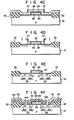
- a thermal oxide film to be serving as a gate oxide film was formed on an element formation region surrounded by the field oxide film 32.
- a polycrystalline silicon film was then deposited to cover the entire surface and was patterned to form a gate electrode 33.
- the thermal oxide film was etched using the gate electrode 33 as a mask, thereby forming a gate oxide film 34.
- arsenic or phosphorus ions were ion-implanted at a dose (in subsequent annealing, diffusion layers having an impurity concentration of 10 16 to 10 18 cm -3 were formed) (Fig. 4A).
- Thermal oxidation was then performed to form a thermal oxide film 35 as a first film on the exposed surface of the substrate 31 and the surface of the gate electrode 33 to a thickness of 400 A (in general, the first film has a thickness of 100 to 500 A).
- a polycrystalline silicon film 36 was deposited to cover the entire surface to a thickness of 0.5 ⁇ m (in general, the polycrystalline silicion film has a thickness of 0.1 to 1 ⁇ m).
- the polycrystalline silicon film had good step coverage for the shape of the gate electrode 33, so that a step portion having substantially vertical walls was obtained.
- the thickness of the polycrystalline silicon film 36 is an important factor to determine a width La of each of the n -type regions of the source and drain regions to be described later, so that the thickness must be accurately controlled.
- Thermal oxidation was then performed to form a thermal oxide film 36 as a second film on the surface of the polycrystalline silicon film 35 to a thickness of 500 A (Fig. 4B).
- the thermal oxide film 37 will be used as a mask in anisotropic etching in the subsequent process and will become an important factor for determining the width L ⁇ of the corresponding n -type region.
- a thickness of this oxide film 37 is smaller than that of the polycrystalline silicon film 37 and falls within the range of 100 to 1,000 A.
- the thermal oxide film 37 was then etched by reactive ion etching (RIE). In this case, residual thermal oxide films 47 were formed on the side walls of the polycrystalline silicon film 36 corresponding to the shape of the gate electrode 33 (Fig. 4C).
- RIE reactive ion etching
- the polycrystalline silicon film 36 is etched by reactive ion etching using the residual thermal oxide films 47 as masks.
- residual polycrystalline silicon films 46 were formed on the walls of the gate electrode 33 through the thermal oxide film 35 while the residual thermal oxide films 47 were respectively left at edges of the residual polycrystalline silicon films 46.
- the residual thermal oxide films 47 prevent side etching of the polycrystalline silicon film 36 when the film 36 is etched, so that the width of each of the residual polycrystalline silicon films 46 is substantially the same as the thickness of the polycrystalline silicon film with good controllability.
- Arsenic or phosphorus was ion-implanted at a high dose using the gate electrode 33 and the residual polycrystalline silicon films 46 as a mask (Fig. 4D).
- the residual polycrystalline silicon films 46 were removed by isotropic etching using fluorine series gas, halogen series gas, or alkali solution (e.g., KOH) as an etchant. At the same time, the residual thermal oxide films 47 were lifted off. Subsequently, thermal annealing was performed to activate ion-implanted layers obtained by performing ion implantation twice, thereby forming a source region 38 comprising an n -type impurity region 38a and an adjoining n +- type impurity region 38b, and a drain region 39 comprising an n -type impurity region 39a and an adjoining n +- type impurity region 39b (Fig. 4E).
- a CVD oxide film 40 was then deposited to cover the entire surface of the resultant structure, and contact holes 41a and 41b were formed in the CVD oxide film 40.
- An aluminum film was deposited to cover the entire surface and was patterned to obtain an aluminum wiring layer 42.
- a MOS semiconductor device having an LDD structure was prepared (Fig. 4F).
- the step portion having substantially vertical walls corresponding to the shape of the gate electrode 33 can be obtained.
- the thermal oxide film 37 as the second film is etched by anisotropic etching to form the residual thermal oxide films 47.
- the polycrystalline silicon film 36 is subjected to anisotropic etching, so that, side etching of the polycrystalline silicon film 36 can be prevented due to the presence of the residual thermal oxide films 47.
- each of the residual polycrystalline silicon films 46 corresponding to the width La of the n -type impurity regions of the source and drain regions can be controlled with high precision.
- the ion-implanted layers formed by ion implantation at a low dose using the gate electrode 33 shown in Fig. 4A as a mask and by ion implantation at a high dose using the gate electrode 33 and the residual polycrystalline silicon films 46 shown in Fig. 4D as masks are activated by annealing in Fig. 4E, each of the n -type impurity regions 38a and 39a of the source and drain regions 38 and 39 can have the designed width L ⁇ (e.g., 0.1 to 1 ⁇ m).
- isotropic etching is performed in the above embodiment using an etchant for polycrystalline silicon.
- an etchant for an oxide may first be used to remove the residual thermal oxide films 47 and then the etchant for poly-silicon may be used to remove the residual polycrystalline silicon films 46.
- care must be taken not to expose the substrate 31 by removing the thermal oxide film 35 on the surface of the substrate 31 when the residual thermal oxide films 47 are etched. This drawback lies in the fact that the portions of the substrate 31 which correspond to the source and drain regions are etched when the residual polycrystalline silicon films 46 are etched.
- the etching process of the residual thermal oxide films 47 allows only a small margin.
- the above embodiment does not have the following drawbacks: the portions of the substrate 31 which correspond to the source and drain regions are not exposed; and the thickness of the field oxide film 32 is not decreased. Etching can be sufficiently performed to increase the margin, and the process can be simplified.
- n-type impurity arsenic or phosphorus is used as the n-type impurity.
- a p-type impurity such as boron can be ion-implanted at a depth greater than that of the n-type impurity, thereby reducing deep diffusion of the n-type impurity and the short channel effect.
- the above embodiment is exemplified by an n-channel MOS type semiconductor device.
- the present invention may also be applied to a p-channel MOS type semiconductor device and a CMOS type semiconductor device.
Landscapes
- Insulated Gate Type Field-Effect Transistor (AREA)
Applications Claiming Priority (2)
| Application Number | Priority Date | Filing Date | Title |
|---|---|---|---|
| JP58011970A JPS59138379A (ja) | 1983-01-27 | 1983-01-27 | 半導体装置の製造方法 |
| JP11970/83 | 1983-01-27 |
Publications (2)
| Publication Number | Publication Date |
|---|---|
| EP0127725A1 true EP0127725A1 (fr) | 1984-12-12 |
| EP0127725B1 EP0127725B1 (fr) | 1987-04-01 |
Family
ID=11792470
Family Applications (1)
| Application Number | Title | Priority Date | Filing Date |
|---|---|---|---|
| EP84100874A Expired EP0127725B1 (fr) | 1983-01-27 | 1984-01-27 | Procédé pour la fabrication d'un dispositif semi-conducteur comportant des régions faiblement dotées |
Country Status (4)
| Country | Link |
|---|---|
| US (1) | US4488351A (fr) |
| EP (1) | EP0127725B1 (fr) |
| JP (1) | JPS59138379A (fr) |
| DE (1) | DE3462969D1 (fr) |
Cited By (5)
| Publication number | Priority date | Publication date | Assignee | Title |
|---|---|---|---|---|
| DE3530065A1 (de) * | 1984-08-22 | 1986-03-06 | Mitsubishi Denki K.K., Tokio/Tokyo | Verfahren zur herstellung eines halbleiters |
| EP0188897A1 (fr) * | 1984-12-21 | 1986-07-30 | Kabushiki Kaisha Toshiba | Procédé de fabrication d'un transistor bipolaire à hétérojonction |
| GB2216144A (en) * | 1987-04-20 | 1989-10-04 | Gen Electric | Method for producing electrical contacts to amorphous silicon |
| EP0399529A1 (fr) * | 1989-05-24 | 1990-11-28 | Kabushiki Kaisha Toshiba | Méthode de fabrication d'un élément semi-conducteur, et élément semi-conducteur ainsi fabriqué |
| US5212105A (en) * | 1989-05-24 | 1993-05-18 | Kabushiki Kaisha Toshiba | Semiconductor device manufacturing method and semiconductor device manufactured thereby |
Families Citing this family (43)
| Publication number | Priority date | Publication date | Assignee | Title |
|---|---|---|---|---|
| USRE32800E (en) * | 1981-12-30 | 1988-12-13 | Sgs-Thomson Microelectronics, Inc. | Method of making mosfet by multiple implantations followed by a diffusion step |
| US4599118A (en) * | 1981-12-30 | 1986-07-08 | Mostek Corporation | Method of making MOSFET by multiple implantations followed by a diffusion step |
| JPH0693494B2 (ja) * | 1984-03-16 | 1994-11-16 | 株式会社日立製作所 | 半導体集積回路装置の製造方法 |
| US5352620A (en) * | 1984-05-23 | 1994-10-04 | Hitachi, Ltd. | Method of making semiconductor device with memory cells and peripheral transistors |
| US4918501A (en) * | 1984-05-23 | 1990-04-17 | Hitachi, Ltd. | Semiconductor device and method of producing the same |
| JPS6116571A (ja) * | 1984-07-03 | 1986-01-24 | Ricoh Co Ltd | 半導体装置の製造方法 |
| US4658496A (en) * | 1984-11-29 | 1987-04-21 | Siemens Aktiengesellschaft | Method for manufacturing VLSI MOS-transistor circuits |
| US4590665A (en) * | 1984-12-10 | 1986-05-27 | Solid State Scientific, Inc. | Method for double doping sources and drains in an EPROM |
| US4585517A (en) * | 1985-01-31 | 1986-04-29 | Motorola, Inc. | Reactive sputter cleaning of semiconductor wafer |
| JPS61191070A (ja) * | 1985-02-20 | 1986-08-25 | Toshiba Corp | 半導体装置の製造方法 |
| US4653173A (en) * | 1985-03-04 | 1987-03-31 | Signetics Corporation | Method of manufacturing an insulated gate field effect device |
| US4649629A (en) * | 1985-07-29 | 1987-03-17 | Thomson Components - Mostek Corp. | Method of late programming a read only memory |
| JPH0740604B2 (ja) * | 1985-07-30 | 1995-05-01 | ソニー株式会社 | Mos半導体装置の製造方法 |
| US4843023A (en) * | 1985-09-25 | 1989-06-27 | Hewlett-Packard Company | Process for forming lightly-doped-drain (LDD) without extra masking steps |
| US4722909A (en) * | 1985-09-26 | 1988-02-02 | Motorola, Inc. | Removable sidewall spacer for lightly doped drain formation using two mask levels |
| US4745086A (en) * | 1985-09-26 | 1988-05-17 | Motorola, Inc. | Removable sidewall spacer for lightly doped drain formation using one mask level and differential oxidation |
| DE3576610D1 (de) * | 1985-12-06 | 1990-04-19 | Ibm | Verfahren zum herstellen eines voellig selbstjustierten feldeffekttransistors. |
| US5247199A (en) * | 1986-01-15 | 1993-09-21 | Harris Corporation | Process for forming twin well CMOS integrated circuits |
| US5028554A (en) * | 1986-07-03 | 1991-07-02 | Oki Electric Industry Co., Ltd. | Process of fabricating an MIS FET |
| US5214302A (en) * | 1987-05-13 | 1993-05-25 | Hitachi, Ltd. | Semiconductor integrated circuit device forming on a common substrate MISFETs isolated by a field oxide and bipolar transistors isolated by a groove |
| US4753898A (en) * | 1987-07-09 | 1988-06-28 | Motorola, Inc. | LDD CMOS process |
| US4907048A (en) * | 1987-11-23 | 1990-03-06 | Xerox Corporation | Double implanted LDD transistor self-aligned with gate |
| JPH01175260A (ja) * | 1987-12-29 | 1989-07-11 | Nec Corp | 絶縁ゲート電界効果トランジスタの製造方法 |
| US4908326A (en) * | 1988-01-19 | 1990-03-13 | Standard Microsystems Corporation | Process for fabricating self-aligned silicide lightly doped drain MOS devices |
| US5238859A (en) * | 1988-04-26 | 1993-08-24 | Kabushiki Kaisha Toshiba | Method of manufacturing semiconductor device |
| JPH0666329B2 (ja) * | 1988-06-30 | 1994-08-24 | 株式会社東芝 | 半導体装置の製造方法 |
| US4978627A (en) * | 1989-02-22 | 1990-12-18 | Advanced Micro Devices, Inc. | Method of detecting the width of lightly doped drain regions |
| JPH02265250A (ja) * | 1989-04-05 | 1990-10-30 | Nec Corp | 半導体装置の製造方法 |
| FR2646291B1 (fr) * | 1989-04-21 | 1991-06-14 | Thomson Hybrides Microondes | Procede de realisation d'un transistor autoaligne |
| US5013675A (en) * | 1989-05-23 | 1991-05-07 | Advanced Micro Devices, Inc. | Method of forming and removing polysilicon lightly doped drain spacers |
| US5030590A (en) * | 1989-06-09 | 1991-07-09 | Applied Materials, Inc. | Process for etching polysilicon layer in formation of integrated circuit structure |
| JP2760068B2 (ja) * | 1989-07-18 | 1998-05-28 | ソニー株式会社 | Mis型半導体装置の製造方法 |
| US5024959A (en) * | 1989-09-25 | 1991-06-18 | Motorola, Inc. | CMOS process using doped glass layer |
| US5200351A (en) * | 1989-10-23 | 1993-04-06 | Advanced Micro Devices, Inc. | Method of fabricating field effect transistors having lightly doped drain regions |
| US5102816A (en) * | 1990-03-27 | 1992-04-07 | Sematech, Inc. | Staircase sidewall spacer for improved source/drain architecture |
| EP0456318B1 (fr) * | 1990-05-11 | 2001-08-22 | Koninklijke Philips Electronics N.V. | Procédé du type CMOS utilisant des espaceurs de nitrure de silicium placés temporairement pour faire des transistors à drains faiblement dopés |
| JP3380117B2 (ja) * | 1995-07-24 | 2003-02-24 | セイコーインスツルメンツ株式会社 | 半導体装置とその製造方法 |
| TW339470B (en) * | 1997-09-01 | 1998-09-01 | United Microelectronics Corp | The manufacturing method for spacer |
| US5994239A (en) * | 1997-12-18 | 1999-11-30 | Advanced Micro Devices, Inc. | Manufacturing process to eliminate polystringers in high density nand-type flash memory devices |
| US6063668A (en) * | 1997-12-18 | 2000-05-16 | Advanced Micro Devices, Inc. | Poly I spacer manufacturing process to eliminate polystringers in high density nand-type flash memory devices |
| US6281078B1 (en) | 1997-12-18 | 2001-08-28 | Advanced Micro Devices, Inc. | Manufacturing process to eliminate ONO fence material in high density NAND-type flash memory devices |
| US6093610A (en) * | 1998-06-16 | 2000-07-25 | Texas Instruments Incorporated | Self-aligned pocket process for deep sub-0.1 μm CMOS devices and the device |
| US7022596B2 (en) * | 2003-12-30 | 2006-04-04 | Advanced Micro Devices, Inc. | Method for forming rectangular-shaped spacers for semiconductor devices |
Citations (2)
| Publication number | Priority date | Publication date | Assignee | Title |
|---|---|---|---|---|
| DE3131746A1 (de) * | 1980-08-12 | 1982-03-25 | Tokyo Shibaura Denki K.K., Kawasaki, Kanagawa | "verfahren zur herstellung einer halbleitereinheit" |
| US4356623A (en) * | 1980-09-15 | 1982-11-02 | Texas Instruments Incorporated | Fabrication of submicron semiconductor devices |
Family Cites Families (4)
| Publication number | Priority date | Publication date | Assignee | Title |
|---|---|---|---|---|
| JPS54115085A (en) * | 1978-02-28 | 1979-09-07 | Cho Lsi Gijutsu Kenkyu Kumiai | Method of fabricating semiconductor |
| US4209350A (en) * | 1978-11-03 | 1980-06-24 | International Business Machines Corporation | Method for forming diffusions having narrow dimensions utilizing reactive ion etching |
| US4337132A (en) * | 1980-11-14 | 1982-06-29 | Rockwell International Corporation | Ion etching process with minimized redeposition |
| US4432132A (en) * | 1981-12-07 | 1984-02-21 | Bell Telephone Laboratories, Incorporated | Formation of sidewall oxide layers by reactive oxygen ion etching to define submicron features |
-
1983
- 1983-01-27 JP JP58011970A patent/JPS59138379A/ja active Granted
-
1984
- 1984-01-25 US US06/573,654 patent/US4488351A/en not_active Expired - Lifetime
- 1984-01-27 DE DE8484100874T patent/DE3462969D1/de not_active Expired
- 1984-01-27 EP EP84100874A patent/EP0127725B1/fr not_active Expired
Patent Citations (3)
| Publication number | Priority date | Publication date | Assignee | Title |
|---|---|---|---|---|
| DE3131746A1 (de) * | 1980-08-12 | 1982-03-25 | Tokyo Shibaura Denki K.K., Kawasaki, Kanagawa | "verfahren zur herstellung einer halbleitereinheit" |
| US4356623A (en) * | 1980-09-15 | 1982-11-02 | Texas Instruments Incorporated | Fabrication of submicron semiconductor devices |
| US4356623B1 (fr) * | 1980-09-15 | 1989-07-25 |
Non-Patent Citations (2)
| Title |
|---|
| IEEE JOURNAL OF SOLID-STATE CIRCUITS, vol. SC-15, no. 4, August 1980, pages 424-432, New York, USA * |
| IEEE JOURNAL OF SOLID-STATE CIRCUITS, vol. SC-17, no. 2, April 1982, pages 220-226, New York, USA * |
Cited By (9)
| Publication number | Priority date | Publication date | Assignee | Title |
|---|---|---|---|---|
| DE3530065A1 (de) * | 1984-08-22 | 1986-03-06 | Mitsubishi Denki K.K., Tokio/Tokyo | Verfahren zur herstellung eines halbleiters |
| US4727038A (en) * | 1984-08-22 | 1988-02-23 | Mitsubishi Denki Kabushiki Kaisha | Method of fabricating semiconductor device |
| DE3530065C2 (de) * | 1984-08-22 | 1999-11-18 | Mitsubishi Electric Corp | Verfahren zur Herstellung eines Halbleiters |
| EP0188897A1 (fr) * | 1984-12-21 | 1986-07-30 | Kabushiki Kaisha Toshiba | Procédé de fabrication d'un transistor bipolaire à hétérojonction |
| US4679305A (en) * | 1984-12-21 | 1987-07-14 | Kabushiki Kaisha Toshiba | Method of manufacturing a heterojunction bipolar transistor having self-aligned emitter and base and selective isolation regions |
| GB2216144A (en) * | 1987-04-20 | 1989-10-04 | Gen Electric | Method for producing electrical contacts to amorphous silicon |
| GB2216144B (en) * | 1987-04-20 | 1991-07-10 | Gen Electric | Method for producing electrical contacts to amorphous silicon |
| EP0399529A1 (fr) * | 1989-05-24 | 1990-11-28 | Kabushiki Kaisha Toshiba | Méthode de fabrication d'un élément semi-conducteur, et élément semi-conducteur ainsi fabriqué |
| US5212105A (en) * | 1989-05-24 | 1993-05-18 | Kabushiki Kaisha Toshiba | Semiconductor device manufacturing method and semiconductor device manufactured thereby |
Also Published As
| Publication number | Publication date |
|---|---|
| EP0127725B1 (fr) | 1987-04-01 |
| JPH0434819B2 (fr) | 1992-06-09 |
| US4488351A (en) | 1984-12-18 |
| JPS59138379A (ja) | 1984-08-08 |
| DE3462969D1 (en) | 1987-05-07 |
Similar Documents
| Publication | Publication Date | Title |
|---|---|---|
| US4488351A (en) | Method for manufacturing semiconductor device | |
| US4757026A (en) | Source drain doping technique | |
| EP0164449B1 (fr) | Procédé pour fabriquer un dispositif à circuit intégré semi-conducteur comportant un élément du type MISFET | |
| KR0130549B1 (ko) | Cmos 장치의 제조방법 | |
| US5583064A (en) | Semiconductor device and process for formation thereof | |
| GB2197532A (en) | Source drain doping technique | |
| US4784965A (en) | Source drain doping technique | |
| US6087239A (en) | Disposable spacer and method of forming and using same | |
| JP2929419B2 (ja) | 半導体素子の製造方法 | |
| EP0465045A2 (fr) | Procédé pour fabriquer des transistors à effet de champ pour circuits intégrés | |
| US5994743A (en) | Semiconductor device having different sidewall widths and different source/drain depths for NMOS & PMOS structures | |
| KR0172262B1 (ko) | 반도체 소자의 제조방법 | |
| US4263057A (en) | Method of manufacturing short channel MOS devices | |
| EP0459398B1 (fr) | Méthode de fabrication du canal d'un dispositif semi-conducteur MOS | |
| US6008100A (en) | Metal-oxide semiconductor field effect transistor device fabrication process | |
| JP3049496B2 (ja) | Mosfetの製造方法 | |
| JPH0147016B2 (fr) | ||
| JP2633104B2 (ja) | 半導体装置の製造方法 | |
| KR0167301B1 (ko) | 모스전계효과트랜지스터 제조방법 | |
| JPH09181313A (ja) | Mosfetの製造方法 | |
| JPH08316477A (ja) | 半導体素子の製造方法 | |
| KR100261166B1 (ko) | 반도체 소자의 제조 방법 | |
| KR100305205B1 (ko) | 반도체소자의제조방법 | |
| KR100406591B1 (ko) | 반도체소자의제조방법 | |
| JPH06244415A (ja) | 半導体装置およびその製造方法 |
Legal Events
| Date | Code | Title | Description |
|---|---|---|---|
| PUAI | Public reference made under article 153(3) epc to a published international application that has entered the european phase |
Free format text: ORIGINAL CODE: 0009012 |
|
| 17P | Request for examination filed |
Effective date: 19840127 |
|
| AK | Designated contracting states |
Designated state(s): DE FR GB |
|
| RTI1 | Title (correction) | ||
| GRAA | (expected) grant |
Free format text: ORIGINAL CODE: 0009210 |
|
| AK | Designated contracting states |
Kind code of ref document: B1 Designated state(s): DE FR GB |
|
| ET | Fr: translation filed | ||
| REF | Corresponds to: |
Ref document number: 3462969 Country of ref document: DE Date of ref document: 19870507 |
|
| PLBE | No opposition filed within time limit |
Free format text: ORIGINAL CODE: 0009261 |
|
| STAA | Information on the status of an ep patent application or granted ep patent |
Free format text: STATUS: NO OPPOSITION FILED WITHIN TIME LIMIT |
|
| 26N | No opposition filed | ||
| PGFP | Annual fee paid to national office [announced via postgrant information from national office to epo] |
Ref country code: FR Payment date: 19980109 Year of fee payment: 15 |
|
| PGFP | Annual fee paid to national office [announced via postgrant information from national office to epo] |
Ref country code: GB Payment date: 19980119 Year of fee payment: 15 |
|
| PGFP | Annual fee paid to national office [announced via postgrant information from national office to epo] |
Ref country code: DE Payment date: 19980202 Year of fee payment: 15 |
|
| PG25 | Lapsed in a contracting state [announced via postgrant information from national office to epo] |
Ref country code: GB Free format text: LAPSE BECAUSE OF NON-PAYMENT OF DUE FEES Effective date: 19990127 |
|
| GBPC | Gb: european patent ceased through non-payment of renewal fee |
Effective date: 19990127 |
|
| PG25 | Lapsed in a contracting state [announced via postgrant information from national office to epo] |
Ref country code: FR Free format text: LAPSE BECAUSE OF NON-PAYMENT OF DUE FEES Effective date: 19990930 |
|
| PG25 | Lapsed in a contracting state [announced via postgrant information from national office to epo] |
Ref country code: DE Free format text: LAPSE BECAUSE OF NON-PAYMENT OF DUE FEES Effective date: 19991103 |
|
| REG | Reference to a national code |
Ref country code: FR Ref legal event code: ST |