EP0129217A2 - Circuit à semiconducteur comportant une memoire et un circuit d'attaque pour impulsions - Google Patents
Circuit à semiconducteur comportant une memoire et un circuit d'attaque pour impulsions Download PDFInfo
- Publication number
- EP0129217A2 EP0129217A2 EP84106818A EP84106818A EP0129217A2 EP 0129217 A2 EP0129217 A2 EP 0129217A2 EP 84106818 A EP84106818 A EP 84106818A EP 84106818 A EP84106818 A EP 84106818A EP 0129217 A2 EP0129217 A2 EP 0129217A2
- Authority
- EP
- European Patent Office
- Prior art keywords
- voltage
- primary
- pulse
- transistor
- circuit
- Prior art date
- Legal status (The legal status is an assumption and is not a legal conclusion. Google has not performed a legal analysis and makes no representation as to the accuracy of the status listed.)
- Granted
Links
Images







Classifications
-
- F—MECHANICAL ENGINEERING; LIGHTING; HEATING; WEAPONS; BLASTING
- F23—COMBUSTION APPARATUS; COMBUSTION PROCESSES
- F23L—SUPPLYING AIR OR NON-COMBUSTIBLE LIQUIDS OR GASES TO COMBUSTION APPARATUS IN GENERAL ; VALVES OR DAMPERS SPECIALLY ADAPTED FOR CONTROLLING AIR SUPPLY OR DRAUGHT IN COMBUSTION APPARATUS; INDUCING DRAUGHT IN COMBUSTION APPARATUS; TOPS FOR CHIMNEYS OR VENTILATING SHAFTS; TERMINALS FOR FLUES
- F23L9/00—Passages or apertures for delivering secondary air for completing combustion of fuel
-
- H—ELECTRICITY
- H03—ELECTRONIC CIRCUITRY
- H03K—PULSE TECHNIQUE
- H03K19/00—Logic circuits, i.e. having at least two inputs acting on one output; Inverting circuits
- H03K19/01—Modifications for accelerating switching
- H03K19/017—Modifications for accelerating switching in field-effect transistor circuits
- H03K19/01707—Modifications for accelerating switching in field-effect transistor circuits in asynchronous circuits
-
- F—MECHANICAL ENGINEERING; LIGHTING; HEATING; WEAPONS; BLASTING
- F23—COMBUSTION APPARATUS; COMBUSTION PROCESSES
- F23Q—IGNITION; EXTINGUISHING-DEVICES
- F23Q11/00—Arrangement of catalytic igniters
-
- F—MECHANICAL ENGINEERING; LIGHTING; HEATING; WEAPONS; BLASTING
- F24—HEATING; RANGES; VENTILATING
- F24B—DOMESTIC STOVES OR RANGES FOR SOLID FUELS; IMPLEMENTS FOR USE IN CONNECTION WITH STOVES OR RANGES
- F24B13/00—Details solely applicable to stoves or ranges burning solid fuels
- F24B13/02—Arrangement or mountings of fire-grate assemblies; Arrangement or mountings of linings for fire-boxes, e.g. fire-backs
-
- H—ELECTRICITY
- H03—ELECTRONIC CIRCUITRY
- H03K—PULSE TECHNIQUE
- H03K19/00—Logic circuits, i.e. having at least two inputs acting on one output; Inverting circuits
- H03K19/0175—Coupling arrangements; Interface arrangements
- H03K19/0185—Coupling arrangements; Interface arrangements using field effect transistors only
- H03K19/018507—Interface arrangements
-
- F—MECHANICAL ENGINEERING; LIGHTING; HEATING; WEAPONS; BLASTING
- F23—COMBUSTION APPARATUS; COMBUSTION PROCESSES
- F23M—CASINGS, LININGS, WALLS OR DOORS SPECIALLY ADAPTED FOR COMBUSTION CHAMBERS, e.g. FIREBRIDGES; DEVICES FOR DEFLECTING AIR, FLAMES OR COMBUSTION PRODUCTS IN COMBUSTION CHAMBERS; SAFETY ARRANGEMENTS SPECIALLY ADAPTED FOR COMBUSTION APPARATUS; DETAILS OF COMBUSTION CHAMBERS, NOT OTHERWISE PROVIDED FOR
- F23M2900/00—Special features of, or arrangements for combustion chambers
- F23M2900/05004—Special materials for walls or lining
Definitions
- the present invention relates to a pulse control circuit which is suitable for driving a capacitance load at high speed.
- FIG. 1A is taken from U.S. Patent Application No. 368,162 applied for by the present Applicant.
- a miniaturized element 12a of Fig. 1B is used in an internal circuit a which determines the effective integration density of chips 10, and the remedy for the reduction in the voltage resistance resulting from miniaturization is to operate the element by a voltage V DP which is the external supply voltage Vcc reduced by a voltage limiter 30.
- V DP the external supply voltage
- Vcc reduced by a voltage limiter 30.
- V DP the external supply voltage
- Vcc reduced by a voltage limiter 30.
- a comparatively large chip 12b as shown in Fig. 1B, is used for the driving circuit b which is operated by applying Vcc thereto.
- a chip is a single substrate on which memory, logic or other LSI devices are fabricated.
- a is a memory array and its related circuits; and in a logic LSI device, a is an area constructed of repeated cells making up the ROM or RAM area of a microcomputer. Details of embodiments of voltage limiters using this voltage limiter system are given in U.S. Patent Application No. 368,162 and 562,969.
- the output V DP of the voltage limiter 30 is supplied to the drain of a charging transistor as a supply voltage and, pulses of the same level as that of the external supply voltage Vcc is applied to the gate of the transistor, turning the transistor on.
- a precharge circuit for a data line of a semiconductor memory is shown as an example of this type of circuit.
- charging transistors Q 6 , Q 7 controlled by precharge pulse ⁇ p2 of a maximum level of Vcc charge data lines Do and Do to a voltage as large as the output voltage V DP of the voltage limiter 30.
- Numeral 1 denotes a memory cell array.
- the equivalent internal resistance of the voltage limiter 30 is connected in series to the equivalent resistances of the charging transistors Q 6 or Q 7 when they are on, and thus it is necessary to make these resistances much smaller to enable charging at a higher speed when there is a larger capacitance load.
- size of the transistors in the voltage limiter 30 and the transistors Q 6 , Q 7 must be larger, and thus it can be understood that it is difficult to drive a large capacitance load faster when there must be a high degree of integration.
- An object of the present invention is to provide a pulse drive circuit which is suitable for driving a large capacitance load at high speed.
- the present invention includes means for converting primary pulses of a primary voltage which is applied as a supply voltage into secondary pulses of a secondary voltage different from the primary voltage, and a switching means to which the secondary pulses are input as control pulses, the primary voltage is applied as a supply voltage, and which applies a voltage controlled by the secondary voltage to a load.
- Fig. 3 shows a fundamental embodiment of the present invention.
- a signal ⁇ ie whose amplitude is controlled by the operation of a pulse-generating circuit PG is input to a gate of a MOS transistor QL', and a capacitance load C L connected to the source of the transistor is driven thereby.
- the pulse-generating circuit PG inputs pulse ⁇ i of a maximum voltage equivalent to the supply voltage Vcc.
- An inverted output of a driver 12 to which the input pulse ⁇ i is applied makes a MOS transistor Q D discharge its gate voltage so that its electric potential changes from high to low.
- a bootstrap capacitance acts so that the gate voltage of a transistor Q L is charged by a non-inverted output of the driver 12 so that its low potential becomes a high potential of at least the level of Vcc, turning the transistor Q L on.
- V DP which is different from the external supply voltage Vcc and is applied to the gate of a transistor Q LL so that a voltage of V DP VT is applied to the drain of transistor Q D .
- V T denotes the threshold voltage of each transistor in this embodiment.
- the external supply voltage Vcc is applied to the drain of transistor Q L ', but the capacitance load C L is charged by a voltage of up to V DP ⁇ 2V T which is equal to the high voltage V DP ⁇ V T of the pulse ⁇ ie reduced by the threshold voltage V T of the transistor Q L '.
- V DP ⁇ 2V T the high voltage
- W/L channel width/channel length
- V out (hereinafter, "signal voltage” denotes any voltage on the high electric potential side, without particular limitations)
- the voltage of the pulse ⁇ ie is V in and the threshold voltage of the transistor Q L is V T , V out is generally given by; Accordingly, a control of the output voltage on the high electric potential side can be accomplished by controlling V in which can be defined in response to the essential voltage V out .
- V in it is necessary to generate a voltage which is higher than the required charge voltage by the voltage V T .
- the output voltage V DP of the voltage limiter 30 of Fig. 3 could be modified.
- Fig. 4 discloses an embodiment in which the voltage of V DP ⁇ V T is applied to the capacitance load C Z .
- Fig. 4 differs from Fig. 3 only in that a voltage limiter 30A is designed so that it outputs a voltage V DP + V T which is only V T higher than the output V DP of the voltage limiter 30 of Fig. 3.
- Fig. 4 shows a concrete example of the voltage limiter 30 which outputs V DP from a contact point between a resistor R LM and a series of n diodes D 1 to D.
- the voltage limiter 30 outputs the voltage V DP of which has a characteristic as shown in Fig. 5 with respect to the external supply voltage Vcc.
- V 0 is selectively defined by a value which is less than 5V; and when Vcc is 5V, V DP can be determined to be, for example, 3.5V by this characteristic.
- V 0 is equal to the external supply voltage when the n series-connected diodes D 1 to D n of Fig. 4 start to be turned on.
- the gradient m is defined by the ratio of the resistance R Lm in series with the resistance of the group of diodes D 1 ...D n when on.
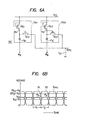
- a high-voltage generation circuit 31 generates a voltage V pp which is higher than the external supply voltage Vcc. This circuit will be described later with reference to Figs. 6A and 6B.
- Fig. 4 two transistors Q 103 , Q 101 , which are arranged so that-the drain of one is connected to the gate of other, and a resistance R p are connected in series between an output terminal of the high-voltage generation circuit 31 and an output terminal of the limiter 30.
- the drain voltage of transistor Q103 is equal to V D+P 2V T . Since this voltage V DP + 2V T is applied to the gate of a transistor Q 102 whose drain receives the external supply voltage Vcc, V DP + V T is applied to the gate of the transistor Q LL in the pulse-generating circuit PG.
- the high electric potential of the pulse ⁇ ie is equal to V DP and so a charging voltage of up to V DP - V T is applied to the capacitance load C L .
- the output voltage V pp of the high-voltage generation circuit 31 is set by the formula:
- a circuit C p1 has a construction and operation such that pulse ⁇ B is applied through a charge-pump capacitor C B to a node between two transistors Q c1 and Q c2 arranged so that the sourceof Q c1 is connected to the gate of Qc2, and pulses higher than Vcc are generated.
- a circuit Cp 2 also comprises of two transistors Q' c1 and Q' c2 connected in the same state as in circuit C p1 and a charge-pump capacitor C' B . However, it differs from C p1 in that pulse ⁇ B is generated.
- ⁇ B and ⁇ B respectively are pulses of a certain period and inverses thereof, in a chip.
- the circuits for producing these pulses are not shown in the drawings for simplicity.
- C p denotes a parasitic capacitance generated in the output wiring.
- Nodes N 1 and N' 1 respectively of transistors Q c1 and Q' c1 of Fig. 6B are precharged to the voltage Vcc ⁇ V T .
- Each of the pulses ⁇ B and ⁇ B then reach Vcc during each of time bands T 1 , T 2' respectively, when the corresponding nodes N 1 and N' 1 are raised to 2Vcc ⁇ V T during T 1 and T 2 by the capacitive coupling of charge-punp capacitors C B and C' B , respectively.
- V pp becomes a d.c. voltage which is greater than Vcc.
- the high-voltage generation circuit 31 receives the charges of the capacitors C B , C' B output during both time bands T 1 , T 2 , the ability of the circuit to supply charge is great, and a ripple noise in its output V pp is low.
- F ig. 7 shows an embodiment which can charge the capacitance load.C Z to the voltage V D p.
- the circuit shown in Fig. 7 differs from that of Fig. 4 in that a voltage limiter 30B is constructed so that the output voltage V DP of the voltage limiter 30 is raised to V DP + 2V T .
- the circuit in Fig. 7 differs from that of Fig. 4 in that the drain and gate of a transistor Q 104 are connected in series to transistors Q 101 ⁇ and Q 103 and high voltages V ppA and V ppB generated by voltage generation circuits 31A and 31B are applied to the drain of a transistor Q 102 and a resistor R p , respectively.
- the gate voltage of the transistor Q 103 is made to be V DP + 3V T by activating the transistor Q 104 .
- a voltage which is higher by V T than that in the circuit of Fig. 4 is applied to the gates of transistors Q LL , Q' L , and the capacitance load C L is charged to the voltage V D p.
- the high-voltage generation circuit 31B supplies the transistor Q LL with a voltage V ppB which value is V DP + 2 V T , in order to raise the gate voltage of the transistor Q L , to V DP + V T which is higher than that in Fig. 4.
- the output V ppA from the high-voltage generation circuit 31A must be greater that the drain voltage V DP + 3V T of the transistor Q 103 .
- the voltage limiter 30 varies the output voltage V DP in accordance with the characteristic of Fig..5.
- the output V DP can be charged to the voltage required for the ageing tests by varying the magnitude of Vcc. This change means that the voltage applied to the load capacitance C L can be varied, and thus the ageing tests can be accomplished for the load capacitance C L .
- Vcc when Vcc is near the normal operating voltage 5V, it is better not to change V DP much if Vcc is varied. For this purpose, it is desirable to minimize the gradient m of the characteristic of Fig. 5 as far as possible. Therefore, in the voltage limiter 30 of Figs. 3, 4 and 7, when the external voltage Vcc is greater than Vo', which is greater than the normal operating voltage 5V, it is desirable,as shown in Fig. 8, to generate V DP so that its characteristic varies with respect to the voltage Vcc above the voltage Vo with a gradient m' that is greater than the gradient m when Vcc is between the voltages Vo and Vo'.
- Fig. 9 shows an embodiment in which the capacitance load C L is supplied with a voltage which varies in accordance with the characteristic of Fig. 8.
- Fig. 9 differs from Fig. 7 in that a voltage limiter 30D is used instead of the voltage limiter 30 of Fig. 7.
- the circuit of the voltage limiter 30D is disclosed in U.S. Patent Application Nos. 368,162 and 562,969.
- This voltage limiter 30D outputs a voltage V Dp which has the characteristic shown in Fig. 8. Namely, in Fig. 9, V G (for example, Vcc + 2V T ) is applied to the gate of a transistor Q o of the voltage limiter 30D.
- the magnitude of the voltage V G is selected so that it can turn Q o on.
- the output is defined by a gradient m' ( m' > m ) which is also determined by the ratio of conductance of transistors Q o and Q l , and also by the sum of the conductances of the transistors Q o and Q' l .
- the circuit shown in Fig. 9 differs from that of Fig. 7 in that a high voltage V ppc generated by a high-voltage generation circuit 31C (which will be described later with reference to Figs. 11A and 11B), is applied to the drain of the transistor Q LL .
- the voltage V ppc is selected to have a magnitude greater than that of the gate voltage V DP + V T of the transistor Q LL even if that gate voltage varies.
- the voltage V ppc is applied to the capacitor C L even if the magnitude of V Dp varies.
- the ageing tests of the capacitance load C L can be accomplished by varying Vcc.
- the voltage limiter 30C of Fig. 9 can be used instead of the voltage limiter 30 of Figs. 3, 4 and 7, and it also goes without saying that the high-voltage generation circuits 31A and 31B of Fig. 9 must generate output voltages V ppA and V ppB that are higher than V Dp + 3V T and V Dp +2V T * respectively, even if Vcc varies.
- a pulse-generating circuit PG' shown in Fig.10A, differs from the pulse-generating circuit PG of Fig. 3 only in that it does not have the transistor Q LL .
- Pulse ⁇ BB output from the pulse-generating circuit PG' are connected to the source of a transistor Q BB by a bootstrap capacitor C BB .
- the drain and gate of the transistor Q BB are connected to the external supply voltage Vcc.
- V ppc is precharged to the voltage V CC ⁇ V T by the transistor Q BB .
- an output pulse ⁇ BB starts to rise simultaneously with an output pulse ⁇ ie of the pulse generation circuit PG (Fig. 9).
- the pulse ⁇ BB rises as far as Vcc, and ⁇ il rises to V DP + V T .
- V PPC rises because of the capacitive coupling of C BB .
- the magnitude of C BB is such that the maximum value of V ppc becomes the voltage necessary for obtaining the source voltage V DP + V T of a transistor Q (Fig. 9), that is, a voltage higher than V DP + V T . It is better to employ the voltage generation circuit 31C than a circuit which outputs V ppc continuously, because V ppc is generated only when a pulse ⁇ il is generated, and so the power consumption is reduced.
- the high-voltage generation circuits 31A and 31B can be constructed of the same circuit.
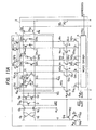
- Figs. 11A and 11B show an embodiment in which the resent invention is applied to MOS dynamic memory with a single ⁇ -transistor type memory cell.
- a group of circuits 1 enclosed within a dot-dash line comprise a memory array circuit.
- a group of circuits 2 enclosed within a dot-dot-dash line comprise circuits (direct peripheral circuits)which control the memory array circuit and amplify signals from memory cells.
- a group of circuits 3 enclosed within a triple-dot dash line denotes circuits (indirect peripheral circuits) which supply signals to the direct peripheral circuits, amplify memory signals from the memory array circuit, and write memory signals into the memory array circuit.
- capacitors C 1 and C 2 , transistors Q 8 , Q 9 and Q 11' Q 12 represent dummy cells.
- Capacitors CM 1 , CM 2 ...CM n-1 , CM n and transistors QM 1 , QM 2 ... QM n-1 , QM n each form memory cells.
- Pulse ⁇ p3 applied to the gates of transistors Q 9 and Q 10 are used to discharge the capacitors C 1 , C 2 before reading, and is generated in a pulse-generating circuit 33.
- A denotes a word driver circuit which generates word-selecting signals from address signals.
- the word driver circuit A raises the gate voltage of a transistor Q 16 on a dummy word line WD 1 to a higher level, and outputs a signal ⁇ xl to a dummy word line WD 1 and the appropriate word line W 1 or W 2 .
- Transistors Q 21' Q 22 connect I/O and I/O lines to data lines D and D by pulses ⁇ 4.
- Transistors Q 1 , Q 2 form part of a sense amplifier and transistors Q 3 , Q 4 act as switches to connect data lines to the sense amplifier.
- Transistors Q 6 , Q 7 are used for precharging and will be described later.
- a transistor Q 5 is used for switching between the short-circuiting of data lines D , D'.
- a transistor Q 18 is used for precharging a line l, and transistors Q 19 , Q 20 are used for driving the sense amplifier.
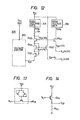
- a voltage limiter 30E outputs two voltages V L1 and V L2 through a circuit shown in Fig. 12. This circuit is formed by connecting the gate of the transistor Q 104 of the voltage limiter 30C of Fig. 9 to the transistor Q 102 of Fig. 4.
- Each transistor is constructed so as to have a threshold voltage V T of 0.5V, and a voltage limiter 30D is constructed so that V DP is 3.5V when the external supply voltage Vcc is 5V.
- V T threshold voltage
- V DP voltage limiter 30D
- the voltage limiter 30E can generate these two voltage magnitudes within a single circuit. Thus, the area of the semiconductor chip acn be reduced, and fluctuations between V L1 and V L2 can be made smaller because the voltage limiter 30E operates on the basis of the same output V DP of the voltage limiter 30D.
- F denotes a circuit in which is inputted a precharge signal ⁇ p2 (5 V) and also V L2 (4.5), and which outputs a precharge signal ⁇ p2l whose voltage is V T less than V L2 .
- F is composed of a circuit which is identical to the pulse-generating circuit PG of Fig.. 9.
- the data lines D, D and a common source terminal of the sense amplifier composed of the transistors Q 1 , Q2 is precharged to a voltage equal to V L2 reduced by only the threshold voltage V T , by transistors Q 6 , Q 7 and Q 18 to the gates of which pulses are applied.
- the precharge voltage is 3.5V.
- these lines can be precharged tc a voltage which is lower than Vcc at high speed.
- the gate voltage ⁇ p1 of Q5 can be made higher than ⁇ p2, transistor Q5 is can be turned on to short-circuit lines D and D.
- I/O, I/O lines are common data input and output lines connected to a plurality of data lines.
- B denotes a pulse-generating circuit
- C denotes another pulse-generating circuit which inputs write data Din and generate pulses din, din which are complementary to each other.
- Numeral 33 denotes a circuit which inputs external control pulse signals at the voltage Vcc and generates pulses such as ⁇ p1 , ⁇ p2 , etc.
- G denotes a circuit which is inputed a signal ⁇ x of a voltage amplitude of 5V and also V L2 (4.5V), and which outpts a signal ⁇ x l of the same voltage amplitude as VL2.
- This circuit shown in Fi g. 13, is well-known and is disclosed in U.S. Patent Application No. 368162 wherein it is described as a circuit for converting a signal amplidute, employing a self- bootstrapping effect.
- This signal ⁇ xi becomes a word line signal of a memory cell.
- the present invention is not applied to the driving circuit G for word lines W 1 ... W n . That is the reason why, since only one word line should be selected and the capacitance thereof is small, the driving speed is made much faster by the circuit G.
- a component in which the present invention is applied must charge all the data lines at once so that the load on it is heavy, and its speed is must therefore be made slower by such means as the driving circuit G. If a data line is charged according to the present invention, it is clearly impossible to make the speed faster than the speed obtained when only one word line is charged by the driving circuit G.
- the present invention is suitable for precharging a large capacitance load such as several data lines, etc., since high-speed charging is not needed.
- H denotes a voltage converter circuit nich is inputed V L1 (4.OV) and Vcc (5V), and which generates a set up d.c. voltage of V cp (3.5V).
- V cp As shown in Fig. 14, it is composed of a so-called source-follower transistor Q ss which inputs Vcc through its drain and V L1 through its gate, and outputs V cp from its source. It is possible to stabilize the operation of the circuit by inserting a large resistance R ss between an output terminal and ground, and by passing a small current therethrough, as shown in Fig. 14.
- V c p is a precharge voltage supplied to the I/O and I/O lines, or it is a writing voltage in the writing circuit composed of transistors Q 23 to Q 26' and is set to 3.5V, equal to the data line voltage.
- a conventional method of inputting the controlled voltage V c p to the drains of transistors Q 28 , Q 29 is employed.
- the I/O, I/O lines can be precharged as fast as the data lines, so the present invention should be applied thereto.
- a circuit such as that shown in Fig. 12 is suitable for this purpose because it has a small capacitance and a convenient layout.
- Fig. 15 shows an embodiment in which a signal ⁇ i-l , an inversion of the signal ⁇ il of Fig. 3, is input to the gate of a transistor Q' D , and an output can be extracted from the drain thereof.
- the inverted signal ⁇ i-l is output and the capacitance load C' L is driven on the basis of the driving ability of a transistor Q D " defined by its W/L ratio.
- any size of driving ability can be obtained by selecting a suitable value of W/L.
- F ig. 16 shows an embodiment in which a push-pull type of buffer circuit is constructed from two of the pulse-generating circuits PG of Fig. 3 which form an inverted signal and apply it and the original signal to the gates of transistors Q L ", Q D ".
- ⁇ il is input to Qz" and the inverted signal ⁇ il of ⁇ il is input to Q D " .
- An output ⁇ o " therefrom is a signal of the same phase as ⁇ il at a voltage controlled by the voltage of ⁇ il .
- the rise term of ⁇ il of ⁇ o " and is output on the basis of the driving ability of transistor Q L " determined by the ratio W/L, and the fall term thereof is output according to that of transistor Q D ".
- the driving ability required for each section can be easily obtained so that the capacitance load C L can be driven at high speed.
- p-channel MOS transistors can be employed of all the potential relationships are reversed.
- the circuit can be operate under conditions in which -5V is applied to the drain of transistor Q L " and OV (ground) is applied to the source of transistor Q D ".
- V in can control V out .
- an operating range of from OV (corresponding to the previous -5V) to 5V (corresponding to the previous OV) is wanted, the whole range can be shifted intact in the positive direction by 5V.
- the output voltage V out in this case is 1.5V (a signal varied by 1.5V on the basis of +5V).
- MOS transistors are used for in a CMOS type of LSI device, and any of the above embodiments can be used therein, according to the purpose of the device.
- Bipolar transistors can be used instead of MOS transistor, the same operations as those of a MOS transistor can be accomplished by a circuit in which the collector, emitter and base of a bipolar transistor replace the drain, source and gate of a MOS transistor, respectively.
- the operating speed depends on the operating and manufacturing conditions because each circuit has a different operating mode, so that it is difficult to maintain this matching.
- the wiring resistances within the memory array circuit 1, the direct peripheral circuits 2, etc. have increased because of the increased integration of memories, and also the characteristics of MOS transistors make it more difficult to match them to the circuits which determine the operating speed.
- FIG. 17 illustrates this state, with reference to an example in which a signal 101a must be generated when the waveform of a signal 100a has fallen below the voltage V crT .
- This is equivalent to the relationship between the discharge speed (100a) for the data lines D , D o during read-out and the signal ⁇ 4 (101a) for extracting those signals onto the I/O line.
- 100b denotes the discharge speed for the data lines D o , D 0 when the external supply voltage V cc drops.
- the discharge speed for a data line is mainly controlled by its wiring resistance
- the time taken for discharge as far as the voltage V crT hardly varies in comparison with the signal waveform of 100a in a memory array in which the integration density and wiring resistance have been increased.
- ⁇ 4 (100a) generated by the peripheral circuits is usually determined by the characteristics of several MOS transistors, the time taken for its generation is greatly delayed, as shown by the signal waveform 101b, when the external supply voltage Vcc drops.
- the signal waveform 101b is generated earlier than that when the signal waveform 100b reaches V crT when the external supply voltage is high.
- Figs. 11A and 11B have been described by way of example, but this method can be applied to any other type of memory with the same objectives, without any modification.
- the present invention can be employed in LSI devices other than memory circuits. It can also be employed in LSI devices which use transistor other than n-type MOS transistors.
Landscapes
- Engineering & Computer Science (AREA)
- General Engineering & Computer Science (AREA)
- Computer Hardware Design (AREA)
- Chemical & Material Sciences (AREA)
- Computing Systems (AREA)
- Mathematical Physics (AREA)
- Physics & Mathematics (AREA)
- Combustion & Propulsion (AREA)
- Mechanical Engineering (AREA)
- Chemical Kinetics & Catalysis (AREA)
- Dram (AREA)
- Static Random-Access Memory (AREA)
- Control Of Indicators Other Than Cathode Ray Tubes (AREA)
Applications Claiming Priority (2)
| Application Number | Priority Date | Filing Date | Title |
|---|---|---|---|
| JP58105710A JPS60694A (ja) | 1983-06-15 | 1983-06-15 | 半導体メモリ |
| JP105710/83 | 1983-06-15 |
Publications (3)
| Publication Number | Publication Date |
|---|---|
| EP0129217A2 true EP0129217A2 (fr) | 1984-12-27 |
| EP0129217A3 EP0129217A3 (en) | 1986-12-03 |
| EP0129217B1 EP0129217B1 (fr) | 1991-11-06 |
Family
ID=14414893
Family Applications (1)
| Application Number | Title | Priority Date | Filing Date |
|---|---|---|---|
| EP84106818A Expired EP0129217B1 (fr) | 1983-06-15 | 1984-06-14 | Circuit à semiconducteur comportant une memoire et un circuit d'attaque pour impulsions |
Country Status (5)
| Country | Link |
|---|---|
| US (1) | US4716313A (fr) |
| EP (1) | EP0129217B1 (fr) |
| JP (1) | JPS60694A (fr) |
| KR (1) | KR920006457B1 (fr) |
| DE (1) | DE3485234D1 (fr) |
Cited By (4)
| Publication number | Priority date | Publication date | Assignee | Title |
|---|---|---|---|---|
| WO1992009141A1 (fr) * | 1990-11-13 | 1992-05-29 | Vlsi Technology, Inc. | Tampon de sortie differentiel |
| WO1992010836A1 (fr) * | 1990-12-12 | 1992-06-25 | Vlsi Technology, Inc. | Tampon precharge avec excursion reduite de la tension de sortie |
| NL9300416A (nl) * | 1992-03-13 | 1993-10-01 | Mitsubishi Electric Corp | Mos transistor uitgangsschakeling. |
| EP0735687A3 (fr) * | 1995-03-31 | 1998-03-25 | STMicroelectronics, Inc. | Circuit d'attaque de sortie avec caractéristiques de commande programmables |
Families Citing this family (28)
| Publication number | Priority date | Publication date | Assignee | Title |
|---|---|---|---|---|
| US5197033A (en) * | 1986-07-18 | 1993-03-23 | Hitachi, Ltd. | Semiconductor device incorporating internal power supply for compensating for deviation in operating condition and fabrication process conditions |
| IT1213431B (it) * | 1986-12-22 | 1989-12-20 | Sgs Microelettronica Spa | Circuito, integrabile monoliticamente, generatore di impulsi di corrente aventi durata brevissima. |
| JPH0728214B2 (ja) * | 1987-02-06 | 1995-03-29 | 株式会社日立製作所 | 半導体集積回路装置 |
| JPH01171194A (ja) * | 1987-12-25 | 1989-07-06 | Nec Ic Microcomput Syst Ltd | 半導体記憶装置 |
| JPH07105448B2 (ja) * | 1988-03-14 | 1995-11-13 | 日本電気株式会社 | Mos型集積回路 |
| JP2883625B2 (ja) * | 1989-03-30 | 1999-04-19 | 株式会社東芝 | Mos型充電回路 |
| JP2809768B2 (ja) * | 1989-11-30 | 1998-10-15 | 株式会社東芝 | 基準電位発生回路 |
| JP2742719B2 (ja) * | 1990-02-16 | 1998-04-22 | 三菱電機株式会社 | 半導体記憶装置 |
| GB2243233A (en) * | 1990-04-06 | 1991-10-23 | Mosaid Inc | DRAM word line driver |
| GB9007790D0 (en) | 1990-04-06 | 1990-06-06 | Lines Valerie L | Dynamic memory wordline driver scheme |
| US5751643A (en) * | 1990-04-06 | 1998-05-12 | Mosaid Technologies Incorporated | Dynamic memory word line driver |
| GB9007791D0 (en) * | 1990-04-06 | 1990-06-06 | Foss Richard C | High voltage boosted wordline supply charge pump and regulator for dram |
| JP2778199B2 (ja) * | 1990-04-27 | 1998-07-23 | 日本電気株式会社 | 内部降圧回路 |
| US5157280A (en) * | 1991-02-13 | 1992-10-20 | Texas Instruments Incorporated | Switch for selectively coupling a power supply to a power bus |
| JP3288727B2 (ja) * | 1991-05-24 | 2002-06-04 | 株式会社東芝 | 出力回路 |
| US5537067A (en) * | 1994-03-11 | 1996-07-16 | Texas Instruments Incorporated | Signal driver circuit operable to control signal rise and fall times |
| US5880593A (en) * | 1995-08-30 | 1999-03-09 | Micron Technology, Inc. | On-chip substrate regulator test mode |
| JP3195913B2 (ja) * | 1996-04-30 | 2001-08-06 | 株式会社東芝 | 半導体集積回路装置 |
| US6198339B1 (en) * | 1996-09-17 | 2001-03-06 | International Business Machines Corporation | CVF current reference with standby mode |
| US5907251A (en) * | 1996-11-22 | 1999-05-25 | International Business Machines Corp. | Low voltage swing capacitive bus driver device |
| US6013958A (en) * | 1998-07-23 | 2000-01-11 | Lucent Technologies Inc. | Integrated circuit with variable capacitor |
| KR100388318B1 (ko) * | 1998-12-24 | 2003-10-10 | 주식회사 하이닉스반도체 | 비트라인디커플링방법 |
| US6212591B1 (en) | 1999-04-02 | 2001-04-03 | Cradle Technologies | Configurable I/O circuitry defining virtual ports |
| US6456152B1 (en) * | 1999-05-17 | 2002-09-24 | Hitachi, Ltd. | Charge pump with improved reliability |
| KR20170076093A (ko) * | 2015-12-24 | 2017-07-04 | 에스케이하이닉스 주식회사 | 반도체 장치 |
| WO2018126337A1 (fr) * | 2017-01-03 | 2018-07-12 | 深圳配天智能技术研究院有限公司 | Appareil de commande de retard à chemins multiples et alimentation électrique de commande |
| JP7565079B2 (ja) * | 2017-09-07 | 2024-10-10 | ヴィスアイシー テクノロジーズ リミテッド | 高電圧高速スイッチング装置 |
| CN110836184B (zh) * | 2018-08-17 | 2022-03-04 | Lg电子株式会社 | 旋转式压缩机 |
Family Cites Families (16)
| Publication number | Priority date | Publication date | Assignee | Title |
|---|---|---|---|---|
| CH558111A (de) * | 1972-07-21 | 1975-01-15 | Battelle Memorial Institute | Circuit generateur de signaux comprenant un oscillateur a quartz delivrant des signaux periodiques biphases et un demultiplicateur de la frequence de ces signaux. |
| JPS52119160A (en) * | 1976-03-31 | 1977-10-06 | Nec Corp | Semiconductor circuit with insulating gate type field dffect transisto r |
| US4065678A (en) * | 1976-07-02 | 1977-12-27 | Motorola, Inc. | Clamped push-pull driver circuit with output feedback |
| JPS5690483A (en) * | 1979-12-19 | 1981-07-22 | Fujitsu Ltd | Address buffer circuit |
| JPS57130294A (en) * | 1981-02-05 | 1982-08-12 | Toshiba Corp | Semiconductor memory |
| DE3105147A1 (de) * | 1981-02-12 | 1982-09-09 | Siemens AG, 1000 Berlin und 8000 München | Integrierte digitale halbleiterschaltung |
| CA1175503A (fr) * | 1981-07-17 | 1984-10-02 | Andreas Demetriou | Circuit d'excitation a cmos |
| US4499387A (en) * | 1981-12-15 | 1985-02-12 | Tokyo Shibaura Denki Kabushiki Kaisha | Integrated circuit formed on a semiconductor substrate with a variable capacitor circuit |
| US4475050A (en) * | 1981-12-21 | 1984-10-02 | Motorola, Inc. | TTL To CMOS input buffer |
| JPS58151124A (ja) * | 1982-03-04 | 1983-09-08 | Ricoh Co Ltd | レベル変換回路 |
| US4469959A (en) * | 1982-03-15 | 1984-09-04 | Motorola, Inc. | Input buffer |
| US4482824A (en) * | 1982-07-12 | 1984-11-13 | Rockwell International Corporation | Tracking ROM drive and sense circuit |
| US4585955B1 (en) * | 1982-12-15 | 2000-11-21 | Tokyo Shibaura Electric Co | Internally regulated power voltage circuit for mis semiconductor integrated circuit |
| US4555642A (en) * | 1983-09-22 | 1985-11-26 | Standard Microsystems Corporation | Low power CMOS input buffer circuit |
| US4584491A (en) * | 1984-01-12 | 1986-04-22 | Motorola, Inc. | TTL to CMOS input buffer circuit for minimizing power consumption |
| US4631426A (en) * | 1984-06-27 | 1986-12-23 | Honeywell Inc. | Digital circuit using MESFETS |
-
1983
- 1983-06-15 JP JP58105710A patent/JPS60694A/ja active Granted
-
1984
- 1984-06-11 KR KR1019840003275A patent/KR920006457B1/ko not_active Expired
- 1984-06-14 DE DE8484106818T patent/DE3485234D1/de not_active Expired - Lifetime
- 1984-06-14 EP EP84106818A patent/EP0129217B1/fr not_active Expired
-
1987
- 1987-06-03 US US07/058,617 patent/US4716313A/en not_active Expired - Lifetime
Cited By (5)
| Publication number | Priority date | Publication date | Assignee | Title |
|---|---|---|---|---|
| WO1992009141A1 (fr) * | 1990-11-13 | 1992-05-29 | Vlsi Technology, Inc. | Tampon de sortie differentiel |
| US5227673A (en) * | 1990-11-13 | 1993-07-13 | Vlsi Technology, Inc. | Differential output buffer with feedback |
| WO1992010836A1 (fr) * | 1990-12-12 | 1992-06-25 | Vlsi Technology, Inc. | Tampon precharge avec excursion reduite de la tension de sortie |
| NL9300416A (nl) * | 1992-03-13 | 1993-10-01 | Mitsubishi Electric Corp | Mos transistor uitgangsschakeling. |
| EP0735687A3 (fr) * | 1995-03-31 | 1998-03-25 | STMicroelectronics, Inc. | Circuit d'attaque de sortie avec caractéristiques de commande programmables |
Also Published As
| Publication number | Publication date |
|---|---|
| KR850000154A (ko) | 1985-02-25 |
| JPH0531236B2 (fr) | 1993-05-12 |
| EP0129217A3 (en) | 1986-12-03 |
| KR920006457B1 (ko) | 1992-08-06 |
| EP0129217B1 (fr) | 1991-11-06 |
| US4716313A (en) | 1987-12-29 |
| DE3485234D1 (de) | 1991-12-12 |
| JPS60694A (ja) | 1985-01-05 |
Similar Documents
| Publication | Publication Date | Title |
|---|---|---|
| US4716313A (en) | Pulse drive circuit | |
| US6232793B1 (en) | Switched backgate bias for FET | |
| US4161040A (en) | Data-in amplifier for an MISFET memory device having a clamped output except during the write operation | |
| US6373315B2 (en) | Signal potential conversion circuit | |
| US7554379B2 (en) | High-speed, low-power level shifter for mixed signal-level environments | |
| EP0655834A1 (fr) | Circuit à retard utilisant une capacité et un transistor | |
| US4616143A (en) | High voltage bootstrapping buffer circuit | |
| JPS6238617A (ja) | 出力回路装置 | |
| US4873673A (en) | Driver circuit having a current mirror circuit | |
| JPH02177716A (ja) | 昇圧回路 | |
| US6072354A (en) | Semiconductor device output buffer circuit for LSI | |
| US9209797B2 (en) | Semiconductor device | |
| US5886942A (en) | Word line driver and semiconductor device | |
| EP0350879B1 (fr) | Circuit tampon de sortie de circuit intégré semi-conducteur | |
| US6084459A (en) | Voltage level shifting circuit | |
| JPH0450770B2 (fr) | ||
| US5148399A (en) | Sense amplifier circuitry selectively separable from bit lines for dynamic random access memory | |
| JP2003273724A (ja) | 半導体集積回路装置 | |
| US4609836A (en) | CMOS transmission circuit | |
| US6147923A (en) | Voltage boosting circuit | |
| US4352996A (en) | IGFET Clock generator circuit employing MOS boatstrap capacitive drive | |
| US6456120B1 (en) | Capacitor-coupling differential logic circuit | |
| US5652727A (en) | Semiconductor memory device | |
| US5737267A (en) | Word line driver circuit | |
| US3965460A (en) | MOS speed-up circuit |
Legal Events
| Date | Code | Title | Description |
|---|---|---|---|
| PUAI | Public reference made under article 153(3) epc to a published international application that has entered the european phase |
Free format text: ORIGINAL CODE: 0009012 |
|
| AK | Designated contracting states |
Designated state(s): DE FR GB IT |
|
| 17P | Request for examination filed |
Effective date: 19841220 |
|
| PUAL | Search report despatched |
Free format text: ORIGINAL CODE: 0009013 |
|
| AK | Designated contracting states |
Kind code of ref document: A3 Designated state(s): DE FR GB IT |
|
| 17Q | First examination report despatched |
Effective date: 19880616 |
|
| GRAA | (expected) grant |
Free format text: ORIGINAL CODE: 0009210 |
|
| AK | Designated contracting states |
Kind code of ref document: B1 Designated state(s): DE FR GB IT |
|
| REF | Corresponds to: |
Ref document number: 3485234 Country of ref document: DE Date of ref document: 19911212 |
|
| ET | Fr: translation filed | ||
| ITF | It: translation for a ep patent filed | ||
| PLBE | No opposition filed within time limit |
Free format text: ORIGINAL CODE: 0009261 |
|
| STAA | Information on the status of an ep patent application or granted ep patent |
Free format text: STATUS: NO OPPOSITION FILED WITHIN TIME LIMIT |
|
| 26N | No opposition filed | ||
| PGFP | Annual fee paid to national office [announced via postgrant information from national office to epo] |
Ref country code: GB Payment date: 20000530 Year of fee payment: 17 |
|
| PGFP | Annual fee paid to national office [announced via postgrant information from national office to epo] |
Ref country code: FR Payment date: 20000619 Year of fee payment: 17 |
|
| PGFP | Annual fee paid to national office [announced via postgrant information from national office to epo] |
Ref country code: DE Payment date: 20000824 Year of fee payment: 17 |
|
| PG25 | Lapsed in a contracting state [announced via postgrant information from national office to epo] |
Ref country code: GB Free format text: LAPSE BECAUSE OF NON-PAYMENT OF DUE FEES Effective date: 20010614 |
|
| GBPC | Gb: european patent ceased through non-payment of renewal fee |
Effective date: 20010614 |
|
| PG25 | Lapsed in a contracting state [announced via postgrant information from national office to epo] |
Ref country code: FR Free format text: LAPSE BECAUSE OF NON-PAYMENT OF DUE FEES Effective date: 20020228 |
|
| PG25 | Lapsed in a contracting state [announced via postgrant information from national office to epo] |
Ref country code: DE Free format text: LAPSE BECAUSE OF NON-PAYMENT OF DUE FEES Effective date: 20020403 |