EP0130496B1 - Dispositif pour indiquer des champs magnétiques - Google Patents
Dispositif pour indiquer des champs magnétiques Download PDFInfo
- Publication number
- EP0130496B1 EP0130496B1 EP84107150A EP84107150A EP0130496B1 EP 0130496 B1 EP0130496 B1 EP 0130496B1 EP 84107150 A EP84107150 A EP 84107150A EP 84107150 A EP84107150 A EP 84107150A EP 0130496 B1 EP0130496 B1 EP 0130496B1
- Authority
- EP
- European Patent Office
- Prior art keywords
- magnetoresistive
- magnetic field
- elements
- negative
- current
- Prior art date
- Legal status (The legal status is an assumption and is not a legal conclusion. Google has not performed a legal analysis and makes no representation as to the accuracy of the status listed.)
- Expired
Links
- 230000005291 magnetic effect Effects 0.000 title claims description 31
- 230000005415 magnetization Effects 0.000 claims description 21
- 230000000694 effects Effects 0.000 claims description 20
- 239000003302 ferromagnetic material Substances 0.000 claims description 8
- 230000001747 exhibiting effect Effects 0.000 claims description 6
- 229910052742 iron Inorganic materials 0.000 claims description 4
- 229910052759 nickel Inorganic materials 0.000 claims description 4
- 229910052741 iridium Inorganic materials 0.000 claims description 2
- GKOZUEZYRPOHIO-UHFFFAOYSA-N iridium atom Chemical compound [Ir] GKOZUEZYRPOHIO-UHFFFAOYSA-N 0.000 claims description 2
- 230000001154 acute effect Effects 0.000 claims 1
- 230000001186 cumulative effect Effects 0.000 claims 1
- 239000000463 material Substances 0.000 description 43
- 239000000956 alloy Substances 0.000 description 11
- 229910045601 alloy Inorganic materials 0.000 description 11
- 239000013598 vector Substances 0.000 description 11
- 230000005294 ferromagnetic effect Effects 0.000 description 10
- 239000000203 mixture Substances 0.000 description 10
- 239000010408 film Substances 0.000 description 8
- PXHVJJICTQNCMI-UHFFFAOYSA-N nickel Substances [Ni] PXHVJJICTQNCMI-UHFFFAOYSA-N 0.000 description 8
- 238000005259 measurement Methods 0.000 description 7
- 229910003271 Ni-Fe Inorganic materials 0.000 description 5
- 230000008859 change Effects 0.000 description 5
- 229910052751 metal Inorganic materials 0.000 description 5
- 239000002184 metal Substances 0.000 description 5
- 239000000758 substrate Substances 0.000 description 4
- 230000007704 transition Effects 0.000 description 4
- 238000009529 body temperature measurement Methods 0.000 description 3
- 150000001875 compounds Chemical class 0.000 description 3
- 230000003993 interaction Effects 0.000 description 3
- 230000005381 magnetic domain Effects 0.000 description 3
- 239000000696 magnetic material Substances 0.000 description 3
- 230000007246 mechanism Effects 0.000 description 3
- 150000002739 metals Chemical class 0.000 description 3
- BASFCYQUMIYNBI-UHFFFAOYSA-N platinum Chemical compound [Pt] BASFCYQUMIYNBI-UHFFFAOYSA-N 0.000 description 3
- 229910017709 Ni Co Inorganic materials 0.000 description 2
- 229910003267 Ni-Co Inorganic materials 0.000 description 2
- 229910003262 Ni‐Co Inorganic materials 0.000 description 2
- 239000002772 conduction electron Substances 0.000 description 2
- 239000004020 conductor Substances 0.000 description 2
- 230000001419 dependent effect Effects 0.000 description 2
- 230000005389 magnetism Effects 0.000 description 2
- 238000000034 method Methods 0.000 description 2
- 239000010948 rhodium Substances 0.000 description 2
- 238000004544 sputter deposition Methods 0.000 description 2
- 229910052723 transition metal Inorganic materials 0.000 description 2
- 150000003624 transition metals Chemical class 0.000 description 2
- 229910020630 Co Ni Inorganic materials 0.000 description 1
- 229910002440 Co–Ni Inorganic materials 0.000 description 1
- 229910001030 Iron–nickel alloy Inorganic materials 0.000 description 1
- 229910018487 Ni—Cr Inorganic materials 0.000 description 1
- XUIMIQQOPSSXEZ-UHFFFAOYSA-N Silicon Chemical compound [Si] XUIMIQQOPSSXEZ-UHFFFAOYSA-N 0.000 description 1
- 239000011248 coating agent Substances 0.000 description 1
- 238000000576 coating method Methods 0.000 description 1
- 238000005260 corrosion Methods 0.000 description 1
- 230000007797 corrosion Effects 0.000 description 1
- 230000008878 coupling Effects 0.000 description 1
- 238000010168 coupling process Methods 0.000 description 1
- 238000005859 coupling reaction Methods 0.000 description 1
- 238000000151 deposition Methods 0.000 description 1
- 230000008021 deposition Effects 0.000 description 1
- 238000001514 detection method Methods 0.000 description 1
- 239000011521 glass Substances 0.000 description 1
- 239000011810 insulating material Substances 0.000 description 1
- 238000004519 manufacturing process Methods 0.000 description 1
- 230000005298 paramagnetic effect Effects 0.000 description 1
- 230000000737 periodic effect Effects 0.000 description 1
- 229910052697 platinum Inorganic materials 0.000 description 1
- 238000002360 preparation method Methods 0.000 description 1
- 229910052703 rhodium Inorganic materials 0.000 description 1
- MHOVAHRLVXNVSD-UHFFFAOYSA-N rhodium atom Chemical compound [Rh] MHOVAHRLVXNVSD-UHFFFAOYSA-N 0.000 description 1
- 229920006395 saturated elastomer Polymers 0.000 description 1
- 239000010703 silicon Substances 0.000 description 1
- 229910052710 silicon Inorganic materials 0.000 description 1
- 230000002277 temperature effect Effects 0.000 description 1
- 239000010409 thin film Substances 0.000 description 1
Images


Classifications
-
- G—PHYSICS
- G11—INFORMATION STORAGE
- G11B—INFORMATION STORAGE BASED ON RELATIVE MOVEMENT BETWEEN RECORD CARRIER AND TRANSDUCER
- G11B5/00—Recording by magnetisation or demagnetisation of a record carrier; Reproducing by magnetic means; Record carriers therefor
- G11B5/127—Structure or manufacture of heads, e.g. inductive
- G11B5/33—Structure or manufacture of flux-sensitive heads, i.e. for reproduction only; Combination of such heads with means for recording or erasing only
- G11B5/39—Structure or manufacture of flux-sensitive heads, i.e. for reproduction only; Combination of such heads with means for recording or erasing only using magneto-resistive devices or effects
- G11B5/3903—Structure or manufacture of flux-sensitive heads, i.e. for reproduction only; Combination of such heads with means for recording or erasing only using magneto-resistive devices or effects using magnetic thin film layers or their effects, the films being part of integrated structures
-
- H—ELECTRICITY
- H10—SEMICONDUCTOR DEVICES; ELECTRIC SOLID-STATE DEVICES NOT OTHERWISE PROVIDED FOR
- H10N—ELECTRIC SOLID-STATE DEVICES NOT OTHERWISE PROVIDED FOR
- H10N50/00—Galvanomagnetic devices
- H10N50/80—Constructional details
- H10N50/85—Materials of the active region
Definitions
- This invention relates to a magnetic field sensing device including a magnetoresistive element exhibiting a negative anisotropic magneto-resistance at room temperature.
- the electrical resistivity p depends on the direction of electrical current through the material with respect to the direction of the saturated magnetization M in the material.
- a resistivity p is measured.
- ⁇ perpendicular
- the resistivities p and p ⁇ differ slightly in magnitudes, and at room temperature it has been found that p ⁇ is greater than p ⁇ .
- This difference in resistivity is the basis for many practical devices using magnetoresistive materials.
- magnetoresistive sensors and field detectors are known in the art in which a sample of magnetoresistive material is used to detect the presence of a magnetic field, such as the magnetic field emanating from a magnetic domain in a tape, disk or a magnetic bubble domain medium.
- the stray magnetic field of the domain intercepts the magnetoresistive sample and causes its magnetization vector to rotate. In turn, this produces a change in the electrical resistivity of the material, which is used as an indication of the presence or absence of the stray magnetic field.
- US ⁇ A ⁇ 3,691,540 describes a magnetoresistive sensor for the detection of magnetic bubble domains.
- MR magnetoresistive
- That patent specification describes different features of MR sensors and discusses them in terms of the anisotropy field H k , the demagnetizing field along a hard axis of the sensor and the thickness of the sensor.
- CH-A-364 296 also discloses a magnetic field sensing device which includes a magnetoresistive element.
- Van Elst did report on a few materials exhibiting -Ap at very low temperatures where the "normal" effect of the electrical resistance of a metal in a magnetic field became important and dominated the typical ferromagnetic effect.
- the quantity Ap can be divided by the average resistivity of the sample to give a quantity ⁇ p/p ave , which is called the anisotropic magnetoresistance ratio.
- p ave is given by Values of ⁇ p range from 0 to 1 micro-ohm cm, in various alloy systems at all temperatures. If Ap and p are limited to room temperatures, the ratio Ap/p can be as high as 3% or 4% in alloys of Ni-Fe and Ni-Co.
- anisotropic magnetoresistance has been discussed in many reference papers including the Van Elst paper referenced above.
- a spin-orbit interaction is invoked. Coupled with this interaction is a variation of the electrical resistance coming from spin-up and spin-down conduction electrons.
- the total scattering cross section of the magnetic atom depends on the angle between the atom's electron spin and the momentum of the scattered conduction electrons.
- the basic mechanism of anisotropic magnetoresistance is complex and it is surprising that Ap remains positive over a huge range of alloys of the type studied in the past 100 years. It is particularly surprising that no materials heretofore have been found which will provide negative Ap of a substantial magnitude at room temperature.
- the ferromagnetic host materials into which Ir is introduced include Ni, Fe, and Co, as well as the room temperature ferromagnetic alloys and compounds of these materials.
- the minimum amount of Ir present in the magnetic material is an amount sufficient to cause negative Ap at room temperature, while the maximum amount is that which would destroy magnetism in the material.
- the range of Ir present in the host material is approximately 1.5-15 atomic percent.
- Such uses include magnetic field detectors and sensors of the type used to detect magnetic domains and magnetic domain transitions in recording media such as tapes and disks.
- a magnetic field sensing device includes, according to the invention, a magnetoresistive element formed from a ferromagnetic material containing at least one of Ni, Fe, and Co, and means to cause an input current to flow through the element in order that the resistance of the element can be sensed, characterised in that the ferromagnetic material also contains Ir in an amount sufficient to cause the element to exhibit, at room temperature, negative anisotropic magnetoresistance (i.e. the resistivity of the element when it is magnetised to saturation in a direction perpendicular to the direction of current flow therethrough is greater than the resistivity of the element when it is magnetised to saturation in a direction parallel to the direction of current flow therethrough).
- negative anisotropic magnetoresistance i.e. the resistivity of the element when it is magnetised to saturation in a direction perpendicular to the direction of current flow therethrough is greater than the resistivity of the element when it is magnetised to saturation in a direction parallel to the direction of current flow therethrough.
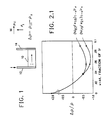
- Fig. 1 shows a magnetoresistive (MR) element 10 to which are attached current carrying leads 12 and 14.
- Current i flows through lead 12 and along the length of MR element 10, returning by conductor lead 14.
- the magnetization M of the MR element 10 is usually in the direction of the current i.
- the resistivity of magnetoresistive element 10 is given by pl .
- the magnetization M of element 10 is rotated to be perpendicular to the direction of current i, the measured resistivity is termed p ⁇ .
- Rotation of the magnetization vector can be caused by, for example, the application of a magnetic field to the element 10 in a direction perpendicular to the current flow through the element.
- the quantity is generally positive for conventional magnetoresistive materials.
- the magnetoresistive element 10 of the present invention exhibits negative ⁇ p at room temperatures and at other temperatures, such as cryogenic temperatures.
- MR element 10 is comprised of certain 3D transition metals which are ferromagnetic, and the alloys and compounds of these metals which are also ferromagnetic, together with Ir.
- the minimum amount of Ir in these ferromagnetic metals, alloys, and compounds is an amount sufficient to cause Ap to be negative.
- very small amounts of Ir are sufficient to cause ⁇ p to be negative. For example, atomic percentages of approximately 3.0 will produce this effect in Ni-Fe and Ni-Co alloys.
- the negative Ap effect is produced by the non-magnetic material (Ir) whose presence deteriorates the magnetic properties of the material to which it is added.
- the exact mechanism for the negative ⁇ p effect is not presently known. The effect is not dependent upon the Hall resistivity of the material, its thickness, method of preparation, or its other magnetic properties.
- Fig. 2.1 shows some examples of Ni-Fe materials exhibiting negative ⁇ p. These are permalloy-type materials having Ir therein in an amount indicated by the horizontal axis. Fig. 2.1 plots the quantity ⁇ p/p against the atomic fraction x of Ir. Two Ni ⁇ Fe compositions are indicated in this Fig.
- these films are approximately 500 nm thick and are prepared on glass or silicon substrates.
- the negative ⁇ p effect does not appear to be thickness or substrate dependent, and different thicknesses and substrates can readily be used in devices embodying the invention.
- the target is generally comprised of two parts.
- the primary metal e.g., Fe, Ni, etc.
- an alloy e.g., Fe-Ni or Co-Ni
- the base On top of this base is placed several pieces of the element (Ir) to be added to the film.
- These substrates generally were rotated on a large plate to allow a more uniform coating of the deposited film thereon.
- these Ni-Fe alloys exhibit a large negative ⁇ p effect. An effect of this magnitude has not heretofore been seen at room temperature.
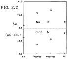
- Fig. 2.2 is a plot of Ap for four different compositions, in a first situation where no Ir is present in the ferromagnetic materials (top curve) and in a second situation where 0.06 atomic fraction of Ir is present in the ferromagnetic materials.
- the four magnetic compositions were pure Fe, Fe 20 Ni 80 , Ni 70 Co 30 , and pure Ni. As is apparent from this Fig. the presence of Ir produces negative Ap while, in the absence of Ir, positive Ap is obtained. These are room temperature measurements.
- Fig. 2.3 plots ⁇ p versus atomic fraction x of Ir for the composition Fe 1-x lr x . These measurements were also made at room temperature. These Fe 1-x lr x compositions produce negative Ap for Ir up to about 15 atomic percent, after which the material becomes paramagnetic with increased Ir content.
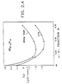
- Fig. 2.4 is a plot of Ap for different atomic fractions x of Ir in a composition comprised of Ni 1-x lr x .
- the top curve is for measurements at room temperature, while the bottom curve is for measurements made at 77°K. From this Fig., it is apparent that Ir even in an amount less than 0.025 atomic fraction, will produce negative ⁇ p in this ferromagnetic material. Above approximately 0.15 atomic fraction, the material loses its magnetism. It should be noted that the curve for data points measured at 77°K indicates a larger magnitude of ⁇ than the room temperature data.
- the following table lists many different magnetoresistive compositions which exhibit large negative ⁇ at room temperature, and which can be used in devices and circuits. Data is shown for both room temperature measurements and low temperature measurements. In measuring the resistivity of these materials, the method of L. J. van der Pauw (cited above) was used. In this table, the thickness t of the films is in nm, the magnetization 4 ⁇ M is in Gauss, and the resistivity p and the anisotropic magneto- resistance ⁇ are in microohms-cms. While many different compositions have been mentioned in this table, it should be understood that some of the data represents an average value for many samples having that composition.
- FIG. 1 shows a basic sensor embodying the present invention
- Figs. 3, 4 and 5 show other representative devices and circuits utilizing the negative ⁇ material, embodying the invention.
- Fig. 3 shows a balanced bridge arrangement containing two magnetoresistive elements 16 and 18.
- Element 16 is comprised of a conventional magnetoresistive material having positive ⁇
- element 18 is comprised of one of the magnetoresistive materials described hereinabove having negative Ap.
- An input current I through lead 20 provides currents i,i' through the elements 16 and 18 respectively in the direction of the arrows 22 and 24.
- the magnitudes of currents i,i' depend on the resistances of elements 16 and 18.
- Conductor leads 26 and 28 return the current, preferably to a differential amplifier 30. When elements 16 and 18 are balanced, the voltage V, is equal to the voltage V 2 and the differential output of amplifier 30 is zero.
- the direction of the magnetization vector M is the same as that of the current through the element, while in element 18 the magnetization vector M is in the opposite direction to that of the current through that element.
- any rotation of the magnetization vectors M due to a magnetic field +H or -H will cause an opposite change in each of the sensing elements.
- the differences between the voltages V 1 and V 2 will be twice as great because a decrease in resistance will occur in one of the elements 16, 18 and an increase in resistance will occur in the other of the elements 16, 18.
- any source of noise due to a temperature change would be suppressed since both elements 16 and 18 would go up or down in resistance together and not interfere with the electrical balance of the circuit.
- Each of the magnetoresistive elements 16 and 18 can be biased to put the magnetization M at a 45° angle with the current flow through each sensing element in order to yield a more linear output.
- the magnetoresistive elements could also be superimposed on each other to reduce the size of the circuit and to provide greater stability from external effects such as temperature-induced noise.
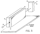
- Figs. 4 and 5 show another circuit in which improved output signals are obtained, while at the same time allowing the coupled elements to be self-biasing (which reduces domain noise).
- two magnetoresistive elements 32 and 34 are located side by side. These elements are typically separated by a thin layer of an insulating material, such as a 10-20 nm thick layer 36 of Si0 2 .
- the sensing elements 32 and 34 are close to one another but are separated by the Si0 2 layer 36 in order to prevent domain interaction between the two elements 32 and 34.
- Element 32 is comprised of a conventional magnetoresistive material exhibiting a positive Ap effect, while element 34 exhibits a negative Ap effect and it is comprised of one of the materials described hereinabove, in which Ir causes negative Ap.
- Fig. 5 illustrates the physical structure and arrangement of the magnetoresistive elements 32 and 34, as well as the insulating layer 36 (Si0 2 ) between them.
- a single lead 38 brings current to both of the elements 32 and 34, while lead 40 is taken from elements 32 and 34 to an amplifier 42, usually a differential amplifier, that provides an output on lead 44.
- a switching field H can have the direction indicated by arrow 1 while the opposite direction is indicated by arrow 2.
- Elements 32 and 34 represent two elements of a coupled magnetoresistive read head. Field H can be produced by transitions in a magnetic recording medium located close to the MR elements 32 and 34, such as tapes and disks.
- the sensing element 34 switches its magnetization into direction 2, which is transverse to the direction of current through that element. Since this is a -Ap material, its resistance will increase. The same magnetic transition will rotate the magnetization vector M into direction 2 in element 32, so that it is in the same direction as that of the current through that element. Since this is a +Ap material, an increase in resistance will occur in this element. The net result is an approximately two-fold increase in resistance compared with the use of a single magnetoresistive element in a sensing head. Again, this accounts for an approximately doubled output from the amplifier 42.
- a configuration such as that shown in Fig. 3 or Figs. 4 and 5 can have other applications, including those of current and magnetic field sensing devices.
- the coupled films 32 and 34 provide a self-biased configuration, so that the magnetization vectors are at -45 0 with respect to the current directions in the films. Additionally, an approximately two-fold increase in output is obtained. Such an increased output would not be obtained if two similar films (i.e., if both films had the same sign of Ap) were used in a parallel arrangement.
Landscapes
- Engineering & Computer Science (AREA)
- Manufacturing & Machinery (AREA)
- Hall/Mr Elements (AREA)
- Measuring Magnetic Variables (AREA)
- Magnetic Heads (AREA)
Claims (11)
Applications Claiming Priority (2)
| Application Number | Priority Date | Filing Date | Title |
|---|---|---|---|
| US509739 | 1983-06-30 | ||
| US06/509,739 US4476454A (en) | 1983-06-30 | 1983-06-30 | New magnetoresistive materials |
Publications (2)
| Publication Number | Publication Date |
|---|---|
| EP0130496A1 EP0130496A1 (fr) | 1985-01-09 |
| EP0130496B1 true EP0130496B1 (fr) | 1986-09-17 |
Family
ID=24027902
Family Applications (1)
| Application Number | Title | Priority Date | Filing Date |
|---|---|---|---|
| EP84107150A Expired EP0130496B1 (fr) | 1983-06-30 | 1984-06-22 | Dispositif pour indiquer des champs magnétiques |
Country Status (4)
| Country | Link |
|---|---|
| US (1) | US4476454A (fr) |
| EP (1) | EP0130496B1 (fr) |
| JP (1) | JPS6011182A (fr) |
| DE (1) | DE3460764D1 (fr) |
Families Citing this family (19)
| Publication number | Priority date | Publication date | Assignee | Title |
|---|---|---|---|---|
| CH659896A5 (de) * | 1982-11-22 | 1987-02-27 | Landis & Gyr Ag | Magnetfeldsensor. |
| DE3346646A1 (de) * | 1983-12-23 | 1985-07-04 | Standard Elektrik Lorenz Ag, 7000 Stuttgart | Magnetfeldsensor |
| DE3435867A1 (de) * | 1984-09-29 | 1986-04-10 | Bosch Gmbh Robert | Differentialsensor |
| US4783711A (en) * | 1985-07-12 | 1988-11-08 | Hitachi, Ltd. | Magnetoresistive sensor having magnetic shields of ferrite |
| JPH06105487B2 (ja) * | 1986-07-14 | 1994-12-21 | 株式会社日立製作所 | 磁気記録装置の信号再生回路 |
| US4879619A (en) * | 1988-03-28 | 1989-11-07 | International Business Machines Corporation | Magnetoresistive read transducer |
| US5218497A (en) * | 1988-12-02 | 1993-06-08 | Hitachi, Ltd. | Magnetic recording-reproducing apparatus and magnetoresistive head having two or more magnetoresistive films for use therewith |
| US5155642A (en) * | 1989-11-29 | 1992-10-13 | International Business Machines Corporation | Anisotropy configuration for longitudinally constrained magnetoresistive transducers |
| US5043693A (en) * | 1990-08-13 | 1991-08-27 | The United States Of America As Represented By The Secretary Of The Navy | Heterogeneous magnetoresistive layer |
| US5277991A (en) * | 1991-03-08 | 1994-01-11 | Matsushita Electric Industrial Co., Ltd. | Magnetoresistive materials |
| US5260652A (en) * | 1992-03-25 | 1993-11-09 | Seagate Technology, Inc. | Magnetoresistive sensor with electrical contacts having variable resistive regions for enhanced sensor sensitivity |
| US5440233A (en) * | 1993-04-30 | 1995-08-08 | International Business Machines Corporation | Atomic layered materials and temperature control for giant magnetoresistive sensor |
| US5576914A (en) * | 1994-11-14 | 1996-11-19 | Read-Rite Corporation | Compact read/write head having biased GMR element |
| US5552778A (en) * | 1994-11-23 | 1996-09-03 | International Business Machines Corporation | Multibit bimorph magnetic tags using acoustic or magnetic interrogation for identification of an object coupled thereto |
| US7123129B1 (en) | 1995-08-14 | 2006-10-17 | Intermec Ip Corp. | Modulation of the resonant frequency of a circuit using an energy field |
| US5812065A (en) | 1995-08-14 | 1998-09-22 | International Business Machines Corporation | Modulation of the resonant frequency of a circuit using an energy field |
| US7002475B2 (en) * | 1997-12-31 | 2006-02-21 | Intermec Ip Corp. | Combination radio frequency identification transponder (RFID tag) and magnetic electronic article surveillance (EAS) tag |
| US6278594B1 (en) | 1998-10-13 | 2001-08-21 | Storage Technology Corporation | Dual element magnetoresistive read head with integral element stabilization |
| US6744086B2 (en) | 2001-05-15 | 2004-06-01 | Nve Corporation | Current switched magnetoresistive memory cell |
Family Cites Families (9)
| Publication number | Priority date | Publication date | Assignee | Title |
|---|---|---|---|---|
| CH364296A (de) * | 1958-02-10 | 1962-09-15 | Siemens Ag | Magnetfeldempfindlicher Widerstand |
| US3691540A (en) * | 1970-10-06 | 1972-09-12 | Ibm | Integrated magneto-resistive sensing of bubble domains |
| FR2165206A5 (fr) * | 1971-12-22 | 1973-08-03 | Cii | |
| JPS5823453B2 (ja) * | 1978-02-27 | 1983-05-16 | ソニー株式会社 | 磁電変換素子用合金及びその製造方法 |
| US4296377A (en) * | 1978-03-27 | 1981-10-20 | Sony Corporation | Magnetic signal field sensor that is substantially immune to angular displacement relative to the signal field |
| NL7804377A (nl) * | 1978-04-25 | 1979-10-29 | Philips Nv | Magnetoweerstandkop. |
| NL7806568A (nl) * | 1978-06-19 | 1979-12-21 | Philips Nv | Magnetoweerstand leeskop. |
| US4242710A (en) * | 1979-01-29 | 1980-12-30 | International Business Machines Corporation | Thin film head having negative magnetostriction |
| JPS5866072A (ja) * | 1981-10-14 | 1983-04-20 | Sanyo Electric Co Ltd | 磁気検出器 |
-
1983
- 1983-06-30 US US06/509,739 patent/US4476454A/en not_active Expired - Fee Related
-
1984
- 1984-03-19 JP JP59051297A patent/JPS6011182A/ja active Granted
- 1984-06-22 DE DE8484107150T patent/DE3460764D1/de not_active Expired
- 1984-06-22 EP EP84107150A patent/EP0130496B1/fr not_active Expired
Non-Patent Citations (1)
| Title |
|---|
| Physica XVI, No. 6, June 1951, pp. 612-627 * |
Also Published As
| Publication number | Publication date |
|---|---|
| JPH0342792B2 (fr) | 1991-06-28 |
| JPS6011182A (ja) | 1985-01-21 |
| US4476454A (en) | 1984-10-09 |
| EP0130496A1 (fr) | 1985-01-09 |
| DE3460764D1 (en) | 1986-10-23 |
Similar Documents
| Publication | Publication Date | Title |
|---|---|---|
| EP0130496B1 (fr) | Dispositif pour indiquer des champs magnétiques | |
| US5193038A (en) | Shorted dual element magnetoresistive reproduce head exhibiting high density signal amplification | |
| JP2651015B2 (ja) | 強磁性薄膜を有する磁場センサ | |
| EP0288766B1 (fr) | Capteur magnétorésistif à film antiferromagnétique | |
| US5014147A (en) | Magnetoresistive sensor with improved antiferromagnetic film | |
| US5677625A (en) | Giant magnetoresistance, production process and application to a magnetic sensor | |
| EP0498668A2 (fr) | Capteur magnétorésistif | |
| JPH04247607A (ja) | 磁気抵抗効果素子 | |
| JPH0950613A (ja) | 磁気抵抗効果素子及び磁界検出装置 | |
| EP1151482A1 (fr) | Capteur a effet tunnel dependant du spin | |
| US6621666B2 (en) | Magnetoresistive-effect element having electrode layers oppositely disposed on main surfaces of a magnetoresistive-effect thin film having hard magnetic bias layers with a particular resistivity | |
| US5521500A (en) | Thin-film magnetic field detector having transverse current and voltage paths intersecting in a common plane | |
| US5696655A (en) | Self-biasing non-magnetic giant magnetoresistance | |
| KR20010078004A (ko) | 자기센서 및 이를 이용한 자기기억장치 | |
| JPH11274599A (ja) | 薄膜磁気抵抗素子 | |
| Mouchot et al. | Magnetoresistive sensors based on Ni/sub 81/Fe/sub 19//Ag multilayers | |
| US5982177A (en) | Magnetoresistive sensor magnetically biased in a region spaced from a sensing region | |
| Gorter et al. | Magnetoresistive reading of information | |
| Dibbern | Sensors based on the magnetoresistive effect | |
| JP3378549B2 (ja) | 磁気ヘッド | |
| JPS6064484A (ja) | 強磁性磁気抵抗効果合金膜 | |
| EP0755086A2 (fr) | Dispositif magnétorésistif | |
| Asama et al. | Ni–Co Film with Large Magnetoresistance for Bubble Detection | |
| JP3873375B2 (ja) | 強磁性金属化合物膜 | |
| RU2831496C1 (ru) | Островковый магниторезистивный датчик |
Legal Events
| Date | Code | Title | Description |
|---|---|---|---|
| PUAI | Public reference made under article 153(3) epc to a published international application that has entered the european phase |
Free format text: ORIGINAL CODE: 0009012 |
|
| AK | Designated contracting states |
Designated state(s): DE FR GB |
|
| 17P | Request for examination filed |
Effective date: 19841123 |
|
| GRAA | (expected) grant |
Free format text: ORIGINAL CODE: 0009210 |
|
| AK | Designated contracting states |
Kind code of ref document: B1 Designated state(s): DE FR GB |
|
| REF | Corresponds to: |
Ref document number: 3460764 Country of ref document: DE Date of ref document: 19861023 |
|
| ET | Fr: translation filed | ||
| PLBE | No opposition filed within time limit |
Free format text: ORIGINAL CODE: 0009261 |
|
| STAA | Information on the status of an ep patent application or granted ep patent |
Free format text: STATUS: NO OPPOSITION FILED WITHIN TIME LIMIT |
|
| 26N | No opposition filed | ||
| PGFP | Annual fee paid to national office [announced via postgrant information from national office to epo] |
Ref country code: DE Payment date: 19890717 Year of fee payment: 6 |
|
| PGFP | Annual fee paid to national office [announced via postgrant information from national office to epo] |
Ref country code: GB Payment date: 19900516 Year of fee payment: 7 |
|
| PGFP | Annual fee paid to national office [announced via postgrant information from national office to epo] |
Ref country code: FR Payment date: 19900529 Year of fee payment: 7 |
|
| PG25 | Lapsed in a contracting state [announced via postgrant information from national office to epo] |
Ref country code: DE Effective date: 19910301 |
|
| PG25 | Lapsed in a contracting state [announced via postgrant information from national office to epo] |
Ref country code: GB Effective date: 19910622 |
|
| GBPC | Gb: european patent ceased through non-payment of renewal fee | ||
| PG25 | Lapsed in a contracting state [announced via postgrant information from national office to epo] |
Ref country code: FR Effective date: 19920228 |
|
| REG | Reference to a national code |
Ref country code: FR Ref legal event code: ST |