EP0130687A2 - Lichtempfindliches Element und Verfahren zur Herstellung dieses Elements - Google Patents
Lichtempfindliches Element und Verfahren zur Herstellung dieses Elements Download PDFInfo
- Publication number
- EP0130687A2 EP0130687A2 EP19840303571 EP84303571A EP0130687A2 EP 0130687 A2 EP0130687 A2 EP 0130687A2 EP 19840303571 EP19840303571 EP 19840303571 EP 84303571 A EP84303571 A EP 84303571A EP 0130687 A2 EP0130687 A2 EP 0130687A2
- Authority
- EP
- European Patent Office
- Prior art keywords
- charge generating
- amine
- coating
- derivatives
- layer
- Prior art date
- Legal status (The legal status is an assumption and is not a legal conclusion. Google has not performed a legal analysis and makes no representation as to the accuracy of the status listed.)
- Granted
Links
Images
Classifications
-
- G—PHYSICS
- G03—PHOTOGRAPHY; CINEMATOGRAPHY; ANALOGOUS TECHNIQUES USING WAVES OTHER THAN OPTICAL WAVES; ELECTROGRAPHY; HOLOGRAPHY
- G03G—ELECTROGRAPHY; ELECTROPHOTOGRAPHY; MAGNETOGRAPHY
- G03G5/00—Recording-members for original recording by exposure, e.g. to light, to heat or to electrons; Manufacture thereof; Selection of materials therefor
- G03G5/02—Charge-receiving layers
- G03G5/04—Photoconductive layers; Charge-generation layers or charge-transporting layers; Additives therefor; Binders therefor
- G03G5/05—Organic bonding materials; Methods for coating a substrate with a photoconductive layer; Inert supplements for use in photoconductive layers
- G03G5/0503—Inert supplements
- G03G5/051—Organic non-macromolecular compounds
- G03G5/0521—Organic non-macromolecular compounds comprising one or more heterocyclic groups
-
- G—PHYSICS
- G03—PHOTOGRAPHY; CINEMATOGRAPHY; ANALOGOUS TECHNIQUES USING WAVES OTHER THAN OPTICAL WAVES; ELECTROGRAPHY; HOLOGRAPHY
- G03G—ELECTROGRAPHY; ELECTROPHOTOGRAPHY; MAGNETOGRAPHY
- G03G5/00—Recording-members for original recording by exposure, e.g. to light, to heat or to electrons; Manufacture thereof; Selection of materials therefor
- G03G5/02—Charge-receiving layers
- G03G5/04—Photoconductive layers; Charge-generation layers or charge-transporting layers; Additives therefor; Binders therefor
-
- G—PHYSICS
- G03—PHOTOGRAPHY; CINEMATOGRAPHY; ANALOGOUS TECHNIQUES USING WAVES OTHER THAN OPTICAL WAVES; ELECTROGRAPHY; HOLOGRAPHY
- G03G—ELECTROGRAPHY; ELECTROPHOTOGRAPHY; MAGNETOGRAPHY
- G03G5/00—Recording-members for original recording by exposure, e.g. to light, to heat or to electrons; Manufacture thereof; Selection of materials therefor
- G03G5/02—Charge-receiving layers
- G03G5/04—Photoconductive layers; Charge-generation layers or charge-transporting layers; Additives therefor; Binders therefor
- G03G5/05—Organic bonding materials; Methods for coating a substrate with a photoconductive layer; Inert supplements for use in photoconductive layers
- G03G5/0503—Inert supplements
- G03G5/051—Organic non-macromolecular compounds
- G03G5/0514—Organic non-macromolecular compounds not comprising cyclic groups
Definitions
- This invention relates to a light-sensitive member (particularly a light-sensitive member for electrophotography) and a method for preparing the same.
- a substance capable of generating carriers by absorption of a visible light can difficultly itself form a film except for very few substances such as amorphous selenium and, moreover, has the drawback of having poor retentive force for the charges given to its surface.
- a substance excellent in film-forming ability and capable of retaining charges of 500 V or higher for a long time with a thickness of about 10 um has generally the drawback of having no sufficient photoconductivity by absorption of a visible light.
- the carrier generating layer may include the case containing a resin and the case containing no resin, but improvement of sensitivity is desired in either case.
- Japanese Unexamined Patent Publication No. 55643/1977 discloses an example in which an amine is used as the solvent for the purpose of enhancing sensitivity of the light-sensitive member. According to this method, dye substances for generation of carriers soluble in an primary organic amine (azo type dye and squaric acid derivative) are dissolved in a solvent containing an organic primary amine, and the resultant solution is applied on an electroconductive substrate to form a carrier generating layer.
- azo type dye and squaric acid derivative azo type dye and squaric acid derivative
- the amine content in the coating solvent is required to be enough to dissolve completely the azo type dye, namely in an amount exceeding 20 %.
- the drying time after coating is prolonged and the coated product after drying is also inconvenient in handling on account of the sticky surface of the carrier generating layer, etc.
- many organic amines have strong stimulating odors and therefore use of much amount of an amine will worsen the environmental conditions during coating.
- the performance of an azo type dye is determined by its crystalline state, but the azo type dye becomes completely amorphous state because it is coated by dissolving according to such a method as described above, whereby no sufficient performance can be obtained.
- the absorption wavelength of the carrier generating layer is shifted toward the shorter wavelength side to result in great lowering in photosensitivity or great lowering in dark decay or acceptive potential during repeated uses of the light-sensitive member.
- the present inventor has found that the causes for the problems as mentioned above are too large amount of an amine contained in the carrier generating layer as well as the too high amine concentration in the coating solution, as the result of using a large amount of an amine for dissolving a carrier generating substance in the known technique of the prior art as described above.
- An object of the present invention is to provide a light-sensitive member which can eliminate all of the drawbacks of the prior art as mentioned above by setting an amine concentration within a specific range in the charge generating phase (carrier generating layer).
- Another object of the present invention is to provide a method for preparing such a photosensitive member with good reproducibility.
- the present invention concerns a light-sensitive member having a charge generating phase containing a charge generating substance, which comprises containing an amine in an amount of not more than 20-fold moles or less of said charge generating substance in said charge generating phase.
- the charge generating substance since the amine' content in the charge generating phase is by far smaller than that in the prior art to be specifically determined as 20-fold or less (desirably 10-fold or less, particularly 5-fold or less) moles of the charge generating substance, the charge generating substance will not substantially be dissolved by the amine during formation of the charge generating phase by coating (that is, the amine does not act as the solvent), but it can be dispersed in a coating solution.
- coating under dispersed state can be rendered possible, whereby the crystallinity in the step of synthesis can be stored and no change in absorption spectrum occurs to improve light sensitivity.
- lowering in dark decay and acceptive potential during repeated use can also effectively be prevented by the amine content as specified above.
- the drying time after coating can be shortened to give no sticky surface and also improve advantageously the environmental maintenance during coating.
- amine content according to the present invention various characteristics such as light sensitivity by amine addition can be improved. This is particularly marked in the case when the charge generating substance has an electron attracting group such as a cyano group in an azo type pigment. Further, within the amine content as specified above, it is possible to effect increase of receiving potential and reduction of dark decay, probably because the amine can be effectively adsorbed on the acceptor site in the charge generating phase, thereby reducing the acceptor concentration to increase the electrical resistance of the charge generating phase.
- the above light-sensitive member according to the present invention should desirably be formed by a process having the step of adding an amine in moles of 20-fold or less of the charge generating substance into a solvent for coating of the charge generating phase and dispersing the charge generating substance in the coating solvent, and the step of forming the charge generating phase by coating of the resultant dispersion.
- the amount of the amine added is preferred to be very small as 1/200 to 1/2000 vol. % (5 ml to 0.5 ml or less per 1000 ml of the solvent for coating solution).
- the charge generating substance may have a molecular weight of 1000, the amine a molecular weight of 80 and the dispersion concentration may be 1.5 % by weight.
- a method for preparation of a light-sensitive member having a charge generating phase (specifically a charge generating layer) and a charge transporting phase (specifically a charge transporting layer) which is in contact with the charge generating layer and contains a charge transporting substance which comprises having the step of adding an amine in moles of 20-fold or less of the charge generating substance into the coating solvent for the charge transporting layer and dissolving the charge transporting substance in the coating solvent and the step of forming the charge transporting layer by coating.
- a predetermined amount (namely within the moles as specified above) of an amine is permitted to be diffused from the coating solution into the charge generating layer, and the amine can be contained in the charge generating layer in an ammount corresponding to said amount.
- the charge generating layer after coating of the aforesaid charge generating layer, can be brought into contact with an amine atmosphere for a predetermiend period of time to have the amine diffused and contained in the charge generating layer in moles as specified above.
- the above amine should desirably have a molecular weight of 150 or less and a basicity ( K ) of 10 -12 or more. It is also preferred to use an B amine having a boiling point higher than the coating solvent for the charge generating phase or for the charge transporting phase being in contact with the charge generating phase. Further, the drying temperature after coating of the charge generating phase or the charge transporting phase should desirably be made lower than the boiling point of the amine.
- phase in addition to the case where a layer is formed, also means the case where both the substances occupy respective regions in a mixture (thereby forming the phases).
- an azo type pigment as the carrier generating substance dipsersed alone or together with a binder resin in a suitable solvent may be coated and dried.
- the azo type pigment which can be utilized in the present invention may include mono-azo type, poly-azo type, metal complex azo type, stilbene azo type, thiazole azo type and the like.
- the azo type dye which can exhibit marked effect of amine addition may include the compounds including electron attracting groups such as CN, Cl, Br, etc. in the mother nucleus as represented by the formulae [I] - [III] shown below.
- a marked effect can also be observed by use of a tris-azo type compound represented by the formula [IV] shown below.
- the amine to be added in a minute amount to a coating solution may comprise primary amines such as monoethanolamine, n-butylamine, ethylenediamine, cyclohexylamine, n-pentylamine, propylamine, iso-butylamine, etc.; secondary amines such as diethanolamine, diethylamine, di-n-propylamine, di-n-butylamine, di-n-pentylamine, di-iso-propylamine, etc.; tertiary amines such as triethanolamine, triethylamine, tributylamine etc.; and heterocyclic amines such as pyridine, piperidine, etc.
- primary amines such as monoethanolamine, n-butylamine, ethylenediamine, cyclohexylamine, n-pentylamine, propylamine, iso-butylamine, etc.
- secondary amines such as diethanolamine, die
- the dispersing medium for an azo type dye may include N,N-dimethylformamide, acetone, methyl ethyl ketone, cyclohexanone, benzene, toluene, xylene, chloroform, 1,2-dichloroethane, dichloromethane, tetrahydrofuran, dioxane, methanol, ethanol, isopropanol, ethyl acetate, butyl acetate, dimethyl sulfoxide and so on.
- the binder resin may include addition polymerization type resins, polyaddition type resins and polycondensation type resins such as polyethylene, polypropylene, acrylic resins, methacrylic resins, vinyl chloride resins, vinyl acetate resins, epoxy resins, polyurethane resins, phenol resins, polyester resins, alkyd resins, polycarbonate resins, silicone resins, melamine resins, etc.
- the proportion of the binder resin to the azo type pigment may desirably be 0 to 100 % by weight, particularly 0 to 10 % by weight.
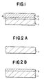
- Fig. 1 illustrates a partial view of a light-sensitive member, comprising a carrier generating layer 2 as described above formed on an electroconductive support 1 and further a carrier transportting layer 3 formed on it.
- a coating solution containing a carrier generating substance dispersed in a solvent containing a minute amount of an amine (20 mole or less of an azo type pigment) is applied on the substrate 1 and dried to form the carrier generating layer 2 as shown in Fig. 2B.
- a coating solution containing a carrier transporting substance is applied on the carrier generating layer 2 and dried to form a carrier transporting layer 3 as shown in Fig. 1.
- the carrier generating layer should have a thickness preferably of 0.05 to 10 um, more preferably 0.05 ⁇ m to 5 ⁇ m. With a thickness less than 0.05 ⁇ m or over 10 um, no sufficient light sensitivity can be obtained.
- the carrier transporting substance to be used in the present invention may be a substance which can transmit sufficiently the light for generating charges in the carrier generating layer on irradiation of light and can also retain the desired charged potential on charging to positive or negative polarity.
- examples of such substances are styryl compounds, hydrazone compounds, oxazole derivatives, oxadiazole derivatives, thiazole derivatives, thiadiazole derivatives, triazole derivatives, imidazole derivatives, imidazolone derivatives, imidazolidine derivatives, bisimidazolidine derivatives, pyrazoline derivatives, oxazolone derivatives, benzothiazole derivatives, benzothiazole derivatives, benzimidazole derivatives, quinazoline derivatives, benzofuran derivatives, acridine derivatives, phenazine derivatives, aminostilbene derivatives, poly-N-vinylcarbazole, poly-l-vinylpyrene, poly-9-viny
- carrier transporting substances may also be added into the above carrier generating layer 2, if desired.
- at least one of the carrier transporting layer and the carrier generating layer may contain the carrier transporitng substance.
- a binder resin may be also contained in the carrier transporting layer in addition to the carrier transporting substance.
- the binder resin may be, for example, polyethylene, polypropylene, acrylic resin, methacrylic resin, polycondensation resin and copolymer resin containing two or more of recurring units of these resins such as vinyl chloride-vinyl acetate resin, vinyl chloride-vinyl acetate-maleic anhydride resin, etc.
- the binder resin is not limited to these resins, but all the resins generally employed for such uses can be employed.
- additives may be inclusive of diphenyl, diphenyl chloride, o-terphenyl, p-terphenyl, dibutyl phthalate, dimethylglycol phthalate, dioctyl phthalate, triphenyl- phosphoric acid, methylnapthalene, benzophenone, chlorinated paraffin, dilaurylthiopropionate, 3,5-dinitrobenzoic acid, various kinds of fluorocarbons, etc.
- a metal plate such as of aluminum or nickel, a metal drum or a metal foil, a plastic film having aluminum, tin oxide or indium oxide vapor deposited thereon or a film or drum of paper or plastic coated with an electroconductive substance may be employed.
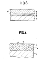
- the light-sensitive member of the present invention may also be constituted as shown in Fig. 3. That is, by providing between the carrier generating layer and the support 1 an intermediate layer 5 as a sub-layer beneath the carrier generating layer 2, the intermediate layer 5 can be endowed with a function to impede injection of free carriers from the electroconductive support 1 into the light-sensitive layer 4, or it can be endowed with an adhesive layer for adhering the light-sensitive layer 4 integrally to the electroconductive support.
- the intermediate layer 5 may be made of a material selected from metal oxides such as aluminum oxide, indium oxide and the like, polymeric compounds such as acrylic resin, methacrylic resin, vinyl chloride resin, vinyl acetate resin, epoxy resin, polyurethane resin, phenol resin, polyester resin, alkyd resin, polycarbonate resin, silicone resin, melamine resin, vinyl chloride-vinyl acetate copolymer resin, vinyl chloride-vinyl acetate-maleic anhydride copolymer resin and the like.
- metal oxides such as aluminum oxide, indium oxide and the like
- polymeric compounds such as acrylic resin, methacrylic resin, vinyl chloride resin, vinyl acetate resin, epoxy resin, polyurethane resin, phenol resin, polyester resin, alkyd resin, polycarbonate resin, silicone resin, melamine resin, vinyl chloride-vinyl acetate copolymer resin, vinyl chloride-vinyl acetate-maleic anhydride copolymer resin and the like.
- the carrier generating layer 2 is formed by coating of a coating solution containing an azo type pigment to which a minute amount of an amine is added, with a composition having an amine content of 20 mole or less of the azo type pigment, and therefore it has a structure which can accomplish sufficiently the object of the present invention.
- a minute amount namely 20 mole or less, preferably 10 mole or less, more preferably 5 mole or less per mole of the azo type pigment
- a minute amount namely 20 mole or less, preferably 10 mole or less, more preferably 5 mole or less per mole of the azo type pigment
- the amount of the amine thus diffused into the carrier can be controlled to 20 mole or less per mole of the azo type pigment similarly as described above.
- the carrier generating layer may be left to stand once in an amine solvent atmosphere for a predetermined period of time thereby attaching an amine on the surface of the carrier generating layer, followed further by diffusion of the amine into the carrier generating layer.
- the amine diffusion concentration into the carrier generating layer can be controlled to set the amine content within the range as specified above.
- Fig. 4 shows an embodiment of a light-sensitive layer 4 comprising two phases in which the particles 6 of the above azo pigment are dispersed in the above carrier transporting substance 7.
- the carrier generating substance 6 should be contained in an amount of 1 to 200 (desirably 10 to 100) parts by weight per 100 parts by weight of the binder. This is because an amount less than 1 part by weight can give only poor sensitivity, while an amount in excess of 200 parts by weight will worsen the film-forming ability.
- the amount of the carrier transporting substance should be 10 to 300 (desirably 50 to 200) parts by weight per 100 parts by weight of the binder. This is because an amount less than 10 parts by weight is poor in the effect, while an amount in excess of 300 parts by weight will lower the film-forming ability and charge retaining ability.
- an electroconductive support made of a polyethylene terephthalate with a thickness of 100 um having aluminum vapor deposited thereon an intermediate layer of a vinyl chloride-vinyl acetate-maleic anhydrice copolymer "Ethlec MF-10" (produced by Sekisui Kagaku Kogyo Co.) with a thickness of about 0.05 ⁇ m was provided.
- a bisazo compound represented by the structural formula [I] shown below was dispersed in 100 ml of a mixed dispersing medium of 1,2-dichloroethane/monoethanolamine of a volume ratio of 1000 : 1 in a ball mill for 8 hours, and the resultant dispersion was applied on the above intermediate layer, followed by sufficient drying, to form a carrier generating layer with a thickness of about 0.3 um.
- Example 1 11.25 g of a styryl compound represented by the structural formula [II] shown below and 15 g of a polycarbonate resin "Panlite L-1250" (produced by Teijin Kasei Co.) were dissolved in 100 ml of 1,2-dichloroethane, and the resulstant solution was applied on the above carrier generating layer, followed by sufficient drying, to form a carrier transporting layer with a thickness of 15 um, thus preparing an electrophotographic light-sensitive member based on the present invention. This is called as "Sample 1".
- Example 1 was repeated except for changing the volume ratio of 1,2-dichloroethane/monoethanolamine as the dispersing medium for coating to 60:1, 110:1, 200:1, 500:1, 5000:1 and 10000:1, respectively, in formation of the carrier generating layer, to prepare 6 kinds of electrophotographic light-sensitive members based on the present invention. These are called as “Sample 2", “Sample 3", “Sample 4", “Sample 5", “Sample 6” and “Sample 7", respectively.
- Example 1 was repeated except for employing as the dispersing medium for coating of the bisazo compound, mixed dispersing media at a volume ratio of 500:1 of 2-dichloroethane/ethylenediamine, l,2-dichloroethane/ piperidine, 1,2-dichloroethane/dietylamine and 1,2-dichloroethane/triethanolamine in formation of the carrier generating layer to prepare 4 kinds of the electrophotographic light-sensitive members based on the present invention. These are called as “Sample 8", “Sample 9", “Sample 10" and “Sample 10", respectively.
- Example 1 was repeated except for employing as the dispersing medium for coating of the bisazo compound, dispersing media 1,2-dichloroethane, monoethanolamine and a mixed dispersing medium at a volume ratio of 50:1 of 2-dichloroethane/monethanolamine in formation of the carrier generating layer to prepare 3 kinds of electrophotographic light-sensitive members for comparative purpose. These are called as “Comparative sample 1", “Comparative sample 2” and “Comparative sample 3", respectively.
- An electrophotographic light-sensitive member based on the present invention was prepared according to entirely the same procedure as in Example 1 except for substituting a trisazo compound represented by the structural formula [III] shown below for charge generating substance of the bisazo compound [I] in formation of the carrier generating layer and substituting a hydrazone compound represented by the structural formula [IV] for the charge transporting substance of the styryl compound [II] in formation of the carrier transporting layer. This is called as "Sample 12".
- Example 12 was repeated except that the volume ratio of 1,2-dichloroethane/monoethanolamine as the mixed dispersing medium for coating of the trisazo compound was changed to 50:1, 100:1, 200:1, 500:1, 5000:1 and 10000:1, respectively, in formation of the carrier generating layer to prepare 6 kinds of electrophotographic light-sensitive members based on the present invention. These are called as “Sample 13", “Sample 14", “Sample 15", “Sample 16", “Sample 17” and “Sample 18", respectively.
- Example 12 was repeated except that, as the mixed dispersing medium for coating of the trisazo compound, 1,2-dichloroethane, monoethanol amine and a mixed dispersing medium of 1,2-dichloroethane/monoethanolamine at a volume ratio of 25:1 were employed, respectively, in formation of the carrier generating layer to prepare 3 kinds of electrophotographic light-sensitive members. These are called as “Comparative sample 4", "Comparative sample 4" and “Comparative sample 5", respectively.
- an intermediate layer of a vinyl chloride-vinyl acetate-maleic anhydrice copolymer "Ethlec MF-10" (produced by Sekisui Kagaku Kogyo Co.) with a thickness of about 0.05 ⁇ m was provided.
- a bisazo compound represented by the structural formula [V] shown below was dispersed in 100 ml of 1,2-dichloroethane in a ball mill for 8 hours, and the resultant dispersion was applied on the above intermediate layer, followed by sufficient drying, to form a carrier generating layer with a thickness of about 0.3 ⁇ m.
- a carrier genearting layer was formed in the same manner as in Example 19, and the carrier generating layer was left to stand in a vapor of monoethanolamine at 120 °c for 5 minutes to treat the carrier generating layer with this vapor, whereby monoethanolamine was diffused into the carrier generating layer.
- a carrier transporting layer was formed similarly as in Example 1 to prepare an electrophotographic light-sensitive member based on the present invention. This is called as "Sample 20".
- Example 21 In formation of the carrier generating layer, Example 1 was repeated except for employing a bisazo compound represented by the structural formula [VII] shown below to provide a carrier generating layer with a thickness of 0.5 um. On the other hand, in formation of the carrier transporting layer, Example 1 was repeated except for employing a carrier transporting substance of a hydrazone compound represented by the structural formula [VIII] shown below to form a carrier transporting layer with a thickness of 15 ⁇ m on the above carrier generating layer, thus preparing an electrophotographic light-sensitive member based on the present invention. This is called as "Sample 21".
- An electrophotographic light-sensitive member for comparative purpose was prepared according to entirely the same procedure as in Example 21 except for using 1,2-dichloroethane as the coating solvent for the bisazo compound. This is called as "Comparative sample 7".
- Example 1 In formation of the carrier generating layer, Example 1 was repeated except for employing a bisazo compound represented by the structural formula [IX] shown below to provide a carrier generating layer with a thickness of 0.5 um. On the other hand, in formation of the carrier transporting layer, Example 1 was repeated except for employing a carrier transporting substance of a hydrazone compound represented by the structural formula [X] shown below to form a carrier transporting layer with a thickness of 15 um on the above carrier generating layer, thus preparing an electrophotographic light-sensitive member based on the present invention. This is called as "Sample 22".
- An electrophotographic light-sensitive member was prepared in enirely the same manner as in Example 22 except for using 1,2-dichloroethane as the solvent for coating of the bisazo compound in formation of the carrier generating layer. This is called as "Comparative sample No. 8".
- Example 1 In formation of the carrier generating layer, Example 1 was repeated except for employing a bisazo compound represented by the structural formula [XI] shown below to provide a carrier generating layer with a thickness of 0.5 um. On the other hand, in formation of the carrier transporting layer, Example 1 was repeated except for employing a carrier transporting substance of a styryl compound represented by the structural formula [XII] shown below to form a carrier transporting layer with a thickness of 15 ⁇ m on the above carrier generating layer, thus preparing an electrophotographic light-sensitive member based on the present invention. This is called as "Sample 22".
- An electrophotographic light-sensitive member was prepared in entirely the same manner as in Example 23 except for using 1,2-dichloroethane as the solvent for coating of the bisazo compound in formation of the carrier generating layer. This called as "Comparative sample No. 9".
- Results are shown in the following Table 1. From the results shown in Table 1, it can clearly be seen that by restricting the amine content in the charge generating layer to 20 moles or less, particularly 10 moles or less (further 5 moles or less) per mole of the charge generating substance based on the present inventon, light sensitivity as well as other electrophotographic characteristics such as dark decay can be greatly improved.
Landscapes
- Physics & Mathematics (AREA)
- General Physics & Mathematics (AREA)
- Spectroscopy & Molecular Physics (AREA)
- Photoreceptors In Electrophotography (AREA)
Applications Claiming Priority (2)
| Application Number | Priority Date | Filing Date | Title |
|---|---|---|---|
| JP58093053A JPS59218447A (ja) | 1983-05-26 | 1983-05-26 | 電子写真感光体及びその製造方法 |
| JP93053/83 | 1983-05-26 |
Publications (3)
| Publication Number | Publication Date |
|---|---|
| EP0130687A2 true EP0130687A2 (de) | 1985-01-09 |
| EP0130687A3 EP0130687A3 (en) | 1986-02-05 |
| EP0130687B1 EP0130687B1 (de) | 1991-01-02 |
Family
ID=14071761
Family Applications (1)
| Application Number | Title | Priority Date | Filing Date |
|---|---|---|---|
| EP84303571A Expired - Lifetime EP0130687B1 (de) | 1983-05-26 | 1984-05-25 | Lichtempfindliches Element und Verfahren zur Herstellung dieses Elements |
Country Status (4)
| Country | Link |
|---|---|
| US (1) | US4591542A (de) |
| EP (1) | EP0130687B1 (de) |
| JP (1) | JPS59218447A (de) |
| DE (1) | DE3483797D1 (de) |
Cited By (2)
| Publication number | Priority date | Publication date | Assignee | Title |
|---|---|---|---|---|
| EP0366308A3 (de) * | 1988-10-28 | 1991-04-03 | Lexmark International, Inc. | Organische Photoleiter mit verringerter Ermüdung |
| GB2251086A (en) * | 1990-11-27 | 1992-06-24 | Xerox Corp | Electrophotographic members |
Families Citing this family (2)
| Publication number | Priority date | Publication date | Assignee | Title |
|---|---|---|---|---|
| US4999267A (en) * | 1988-10-05 | 1991-03-12 | Minolta Camera Kabushiki Kaisha | Photosensitive member having phthalocyanine compound and additive |
| JP2990705B2 (ja) * | 1989-10-05 | 1999-12-13 | ミノルタ株式会社 | 積層型感光体 |
Family Cites Families (10)
| Publication number | Priority date | Publication date | Assignee | Title |
|---|---|---|---|---|
| BE617025A (de) * | 1961-05-01 | |||
| BE754734A (fr) * | 1969-08-28 | 1971-01-18 | Ricoh Kk | Methode de preparation d'un materiau de copie electrophotographique |
| DE2635887C3 (de) * | 1975-09-15 | 1981-11-19 | International Business Machines Corp., 10504 Armonk, N.Y. | Verfahren zur Herstellung eines elektrophotographischen Aufzeichnungsmaterial |
| US4251615A (en) * | 1975-09-19 | 1981-02-17 | Scm Corporation | Viscosity stabilized photoconductive coating material and sheet material using same |
| JPS5640839A (en) * | 1979-09-13 | 1981-04-17 | Canon Inc | Electrophotographic receptor |
| JPS5647043A (en) * | 1979-09-25 | 1981-04-28 | Canon Inc | Electrophotographic receptor |
| US4399206A (en) * | 1980-10-06 | 1983-08-16 | Canon Kabushiki Kaisha | Disazo electrophotographic photosensitive member |
| US4440845A (en) * | 1981-06-08 | 1984-04-03 | Ricoh Co., Ltd. | Disazo compound, method of making same and electrophotographic element using same |
| EP0078151B1 (de) * | 1981-10-23 | 1986-03-12 | Konica Corporation | Photorezeptoren für die Elektrophotographie |
| US4456671A (en) * | 1981-12-23 | 1984-06-26 | Canon Kabushiki Kaisha | Electrophotographic photosensitive member having a photosensitive layer containing a hydrazone compound |
-
1983
- 1983-05-26 JP JP58093053A patent/JPS59218447A/ja active Granted
-
1984
- 1984-05-21 US US06/612,373 patent/US4591542A/en not_active Expired - Lifetime
- 1984-05-25 EP EP84303571A patent/EP0130687B1/de not_active Expired - Lifetime
- 1984-05-25 DE DE8484303571T patent/DE3483797D1/de not_active Expired - Fee Related
Cited By (4)
| Publication number | Priority date | Publication date | Assignee | Title |
|---|---|---|---|---|
| EP0366308A3 (de) * | 1988-10-28 | 1991-04-03 | Lexmark International, Inc. | Organische Photoleiter mit verringerter Ermüdung |
| GB2251086A (en) * | 1990-11-27 | 1992-06-24 | Xerox Corp | Electrophotographic members |
| US5164276A (en) * | 1990-11-27 | 1992-11-17 | Xerox Corporation | Charge generation layers and charge transport, layers for electrophotographic imaging members, and processes for producing same |
| GB2251086B (en) * | 1990-11-27 | 1995-02-01 | Xerox Corp | Electrophotographic imaging members,and processes for producing same |
Also Published As
| Publication number | Publication date |
|---|---|
| EP0130687B1 (de) | 1991-01-02 |
| DE3483797D1 (de) | 1991-02-07 |
| US4591542A (en) | 1986-05-27 |
| EP0130687A3 (en) | 1986-02-05 |
| JPH034901B2 (de) | 1991-01-24 |
| JPS59218447A (ja) | 1984-12-08 |
Similar Documents
| Publication | Publication Date | Title |
|---|---|---|
| US4554231A (en) | Electrophotographic photosensitive member | |
| JPS6028342B2 (ja) | 電子写真感光体 | |
| US4487824A (en) | Electrophotographic photosensitive member containing a halogen substituted hydrazone | |
| US4971874A (en) | Photosensitive member with a styryl charge transporting material | |
| US4591542A (en) | Light-sensitive member and preparation thereof for use in electrophotography | |
| US4900645A (en) | Electrophotographic photosensitive member comprises styryl compound as transport material | |
| JP2811107B2 (ja) | 電子写真感光体 | |
| JP2858167B2 (ja) | 電子写真感光体 | |
| US5077162A (en) | Photosensitive member | |
| US4891289A (en) | Photosensitive member | |
| JP3506071B2 (ja) | 電子写真感光体 | |
| JP2858152B2 (ja) | 電子写真感光体 | |
| JPH08320581A (ja) | 電子写真感光体 | |
| JPH0394258A (ja) | 電子写真感光体 | |
| JP2852787B2 (ja) | 電子写真感光体 | |
| JPH0325776B2 (de) | ||
| JPH0146066B2 (de) | ||
| JP2791497B2 (ja) | 電子写真感光体 | |
| JP2749859B2 (ja) | 電子写真感光体 | |
| JP2601299B2 (ja) | 電子写真感光体 | |
| JPS6017449A (ja) | 感光体 | |
| JPS6059588B2 (ja) | 電子写真感光体 | |
| JPH0118415B2 (de) | ||
| JPH0118421B2 (de) | ||
| JPH0146063B2 (de) |
Legal Events
| Date | Code | Title | Description |
|---|---|---|---|
| PUAI | Public reference made under article 153(3) epc to a published international application that has entered the european phase |
Free format text: ORIGINAL CODE: 0009012 |
|
| AK | Designated contracting states |
Kind code of ref document: A2 Designated state(s): DE FR GB |
|
| PUAL | Search report despatched |
Free format text: ORIGINAL CODE: 0009013 |
|
| AK | Designated contracting states |
Designated state(s): DE FR GB |
|
| 17P | Request for examination filed |
Effective date: 19860616 |
|
| 17Q | First examination report despatched |
Effective date: 19870529 |
|
| RAP3 | Party data changed (applicant data changed or rights of an application transferred) |
Owner name: KONICA CORPORATION |
|
| GRAA | (expected) grant |
Free format text: ORIGINAL CODE: 0009210 |
|
| AK | Designated contracting states |
Kind code of ref document: B1 Designated state(s): DE FR GB |
|
| PG25 | Lapsed in a contracting state [announced via postgrant information from national office to epo] |
Ref country code: FR Effective date: 19910102 |
|
| REF | Corresponds to: |
Ref document number: 3483797 Country of ref document: DE Date of ref document: 19910207 |
|
| EN | Fr: translation not filed | ||
| PLBE | No opposition filed within time limit |
Free format text: ORIGINAL CODE: 0009261 |
|
| STAA | Information on the status of an ep patent application or granted ep patent |
Free format text: STATUS: NO OPPOSITION FILED WITHIN TIME LIMIT |
|
| 26N | No opposition filed | ||
| PGFP | Annual fee paid to national office [announced via postgrant information from national office to epo] |
Ref country code: GB Payment date: 19920429 Year of fee payment: 9 |
|
| PGFP | Annual fee paid to national office [announced via postgrant information from national office to epo] |
Ref country code: DE Payment date: 19920610 Year of fee payment: 9 |
|
| PG25 | Lapsed in a contracting state [announced via postgrant information from national office to epo] |
Ref country code: GB Effective date: 19930525 |
|
| GBPC | Gb: european patent ceased through non-payment of renewal fee |
Effective date: 19930525 |
|
| PG25 | Lapsed in a contracting state [announced via postgrant information from national office to epo] |
Ref country code: DE Effective date: 19940201 |