EP0131341B1 - Méthode de réduction des réflexions dans un écran transparent de visualisation et écran à réflexions réduites - Google Patents
Méthode de réduction des réflexions dans un écran transparent de visualisation et écran à réflexions réduites Download PDFInfo
- Publication number
- EP0131341B1 EP0131341B1 EP84200996A EP84200996A EP0131341B1 EP 0131341 B1 EP0131341 B1 EP 0131341B1 EP 84200996 A EP84200996 A EP 84200996A EP 84200996 A EP84200996 A EP 84200996A EP 0131341 B1 EP0131341 B1 EP 0131341B1
- Authority
- EP
- European Patent Office
- Prior art keywords
- screen
- viewing screen
- vapour
- reflectance
- deposition
- Prior art date
- Legal status (The legal status is an assumption and is not a legal conclusion. Google has not performed a legal analysis and makes no representation as to the accuracy of the status listed.)
- Expired
Links
- 238000000034 method Methods 0.000 title claims description 25
- 239000006117 anti-reflective coating Substances 0.000 claims abstract description 22
- 230000003667 anti-reflective effect Effects 0.000 claims abstract description 5
- 239000010410 layer Substances 0.000 claims description 24
- 238000007788 roughening Methods 0.000 claims description 22
- 238000000151 deposition Methods 0.000 claims description 21
- 239000011248 coating agent Substances 0.000 claims description 20
- 238000000576 coating method Methods 0.000 claims description 20
- ORUIBWPALBXDOA-UHFFFAOYSA-L magnesium fluoride Chemical compound [F-].[F-].[Mg+2] ORUIBWPALBXDOA-UHFFFAOYSA-L 0.000 claims description 13
- 229910001635 magnesium fluoride Inorganic materials 0.000 claims description 13
- 230000003287 optical effect Effects 0.000 claims description 5
- 239000000463 material Substances 0.000 claims description 3
- 238000005498 polishing Methods 0.000 claims description 3
- 239000002356 single layer Substances 0.000 claims description 2
- 238000004544 sputter deposition Methods 0.000 claims description 2
- 238000004519 manufacturing process Methods 0.000 abstract description 3
- 239000011521 glass Substances 0.000 description 16
- 238000002834 transmittance Methods 0.000 description 9
- 238000005530 etching Methods 0.000 description 7
- 230000007704 transition Effects 0.000 description 6
- 230000003014 reinforcing effect Effects 0.000 description 3
- HBMJWWWQQXIZIP-UHFFFAOYSA-N silicon carbide Chemical compound [Si+]#[C-] HBMJWWWQQXIZIP-UHFFFAOYSA-N 0.000 description 3
- XKRFYHLGVUSROY-UHFFFAOYSA-N Argon Chemical compound [Ar] XKRFYHLGVUSROY-UHFFFAOYSA-N 0.000 description 2
- 238000000149 argon plasma sintering Methods 0.000 description 2
- 230000001419 dependent effect Effects 0.000 description 2
- 230000008021 deposition Effects 0.000 description 2
- 230000000694 effects Effects 0.000 description 2
- 238000005516 engineering process Methods 0.000 description 2
- 229910021645 metal ion Inorganic materials 0.000 description 2
- 230000002787 reinforcement Effects 0.000 description 2
- 239000012266 salt solution Substances 0.000 description 2
- 229910010271 silicon carbide Inorganic materials 0.000 description 2
- 238000001228 spectrum Methods 0.000 description 2
- 239000000126 substance Substances 0.000 description 2
- OAICVXFJPJFONN-UHFFFAOYSA-N Phosphorus Chemical compound [P] OAICVXFJPJFONN-UHFFFAOYSA-N 0.000 description 1
- 238000005299 abrasion Methods 0.000 description 1
- 239000002253 acid Substances 0.000 description 1
- 150000007513 acids Chemical class 0.000 description 1
- 230000001154 acute effect Effects 0.000 description 1
- 229910052786 argon Inorganic materials 0.000 description 1
- 230000001427 coherent effect Effects 0.000 description 1
- 230000007423 decrease Effects 0.000 description 1
- 230000001066 destructive effect Effects 0.000 description 1
- 238000010894 electron beam technology Methods 0.000 description 1
- 230000008030 elimination Effects 0.000 description 1
- 238000003379 elimination reaction Methods 0.000 description 1
- 239000007789 gas Substances 0.000 description 1
- 238000007654 immersion Methods 0.000 description 1
- 238000007689 inspection Methods 0.000 description 1
- 238000005342 ion exchange Methods 0.000 description 1
- 150000002500 ions Chemical class 0.000 description 1
- 230000007935 neutral effect Effects 0.000 description 1
- 229910001414 potassium ion Inorganic materials 0.000 description 1
- 238000005070 sampling Methods 0.000 description 1
- 229910001415 sodium ion Inorganic materials 0.000 description 1
- 239000000243 solution Substances 0.000 description 1
- 238000003860 storage Methods 0.000 description 1
- 230000004304 visual acuity Effects 0.000 description 1
Images
Classifications
-
- H—ELECTRICITY
- H04—ELECTRIC COMMUNICATION TECHNIQUE
- H04N—PICTORIAL COMMUNICATION, e.g. TELEVISION
- H04N5/00—Details of television systems
- H04N5/64—Constructional details of receivers, e.g. cabinets or dust covers
- H04N5/65—Holding-devices for protective discs or for picture masks
-
- G—PHYSICS
- G02—OPTICS
- G02B—OPTICAL ELEMENTS, SYSTEMS OR APPARATUS
- G02B1/00—Optical elements characterised by the material of which they are made; Optical coatings for optical elements
- G02B1/10—Optical coatings produced by application to, or surface treatment of, optical elements
- G02B1/11—Anti-reflection coatings
- G02B1/113—Anti-reflection coatings using inorganic layer materials only
-
- H—ELECTRICITY
- H01—ELECTRIC ELEMENTS
- H01J—ELECTRIC DISCHARGE TUBES OR DISCHARGE LAMPS
- H01J29/00—Details of cathode-ray tubes or of electron-beam tubes of the types covered by group H01J31/00
- H01J29/02—Electrodes; Screens; Mounting, supporting, spacing or insulating thereof
- H01J29/10—Screens on or from which an image or pattern is formed, picked up, converted or stored
- H01J29/18—Luminescent screens
- H01J29/24—Supports for luminescent material
-
- H—ELECTRICITY
- H01—ELECTRIC ELEMENTS
- H01J—ELECTRIC DISCHARGE TUBES OR DISCHARGE LAMPS
- H01J29/00—Details of cathode-ray tubes or of electron-beam tubes of the types covered by group H01J31/00
- H01J29/86—Vessels; Containers; Vacuum locks
- H01J29/89—Optical or photographic arrangements structurally combined or co-operating with the vessel
- H01J29/896—Anti-reflection means, e.g. eliminating glare due to ambient light
-
- H—ELECTRICITY
- H01—ELECTRIC ELEMENTS
- H01J—ELECTRIC DISCHARGE TUBES OR DISCHARGE LAMPS
- H01J2229/00—Details of cathode ray tubes or electron beam tubes
- H01J2229/89—Optical components associated with the vessel
- H01J2229/8913—Anti-reflection, anti-glare, viewing angle and contrast improving treatments or devices
- H01J2229/8915—Surface treatment of vessel or device, e.g. controlled surface roughness
-
- H—ELECTRICITY
- H01—ELECTRIC ELEMENTS
- H01J—ELECTRIC DISCHARGE TUBES OR DISCHARGE LAMPS
- H01J2229/00—Details of cathode ray tubes or electron beam tubes
- H01J2229/89—Optical components associated with the vessel
- H01J2229/8913—Anti-reflection, anti-glare, viewing angle and contrast improving treatments or devices
- H01J2229/8918—Anti-reflection, anti-glare, viewing angle and contrast improving treatments or devices by using interference effects
Definitions
- the invention relates to a method of reducing the reflectance of a transparent viewing screen in which firstly the outer surface of the previously formed screen is mechanically roughened and subsequently provided with an anti-reflective coating in such a manner that this coating has a constant thickness and follows the surface profile after roughening.
- the invention also relates to a viewing screen with reduced reflectance, whose outer surface is mechanically roughened and provided with an anti-reflective coating.
- the viewing screen may be the screen of a cathode-ray tube, for example a television picture tube, but alternatively the screen of other display devices, such as a solid-state electroluminescent display device.
- the outer surface of the viewing screen is the side of the screen facing the viewer.
- Display tubes and devices must be suitable for use under high-intensity ambient-light conditions. Since in practice the brightness of a picture on a display tube is limited, the contrast must be as high as possible, so that even in the case of high-intensity ambient-light levels a clearly visible picture is presented to the viewer.
- German Patent Application No. DE-A1-23 21 349 which has been laid open to public inspection, describes a transparent viewing screen, which has a roughened outer surface which is provided with an interference layer with constant thickness.
- the known viewing screen is intended for use as a transparent projection screen.
- United States Patent Specification No. 3,504,212 describes a method of improving the contrast of a television picture tube in which a light-absorbing and light-scattering layer is provided between the phosphor layer and the inner surface of the faceplate. This layer serves to ensure that the ambient light which is incident via the faceplate is no longer reflected to the viewer. Before the light-absorbing layer is deposited the inner surface of the faceplate is frosted or roughened. This is achieved by immersion of the faceplate in an etching bath. This inevitably leads to the outer surface of the faceplate also being roughened.
- the profile on the outer surface of the faceplate as a result of etching has radii which cause a substantial scattering of light and an impermissible reduction in sharpness or definition and contrast of the picture to be reproduced on the faceplate.
- a further process step is applied in which both faceplate surfaces are heated and polished, so as to obtain a satin-type finish.
- the satin-finish outer surface of the faceplate is provided with an anti-reflective coating of magnesium fluoride to reduce residual reflections.
- etching is not a highly favoured process step because it requires special working conditions and because of the storage of the aggressive etching acids. Moreover, an additional process step is required after etching. Also, an additional coating must be applied, so that the method described in United States Patent Specification No. 3,504,212 is rather cumbersome.
- the parameters Ra, Rq, Rtm and Sm are the well-known roughness parameters as specified in standards such as U.S.A.-ANSIB 46.1; U.K. BS 1134 or Netherlands NEN sheets 3631, 3632, 3634, 3637, 3638, which fully define the roughening.
- Elimination of reflection from the viewing screen in accordance with the invention is completely achieved by the combination of surface-roughening and an anti-reflective coating of constant thickness and not primarily by providing an additional coating as in the viewing screens in accordance with German Patent Application No. DE 32 21 349 and United States Patent Specification No. 3,504,212. It has been found that the roughening as specified in the foregoing provides an optimum scattering which in conjunction with the interferometric effect of the thin coating yields a maximum reduction of reflections over the entire range of wavelengths of visible light.
- the inner surface of the viewing screen is also roughened mechanically. This enables the inherently low residual reflectance caused by reflections from the inner surface of the viewing screen to be reduced even further.
- mechanical roughening is effected by using the technique of loose grains on a flexible polishing base.
- the method in accordance with the invention is characterized further in that the anti-reflective coating is formed by vapour-deposition or sputtering in a vacuum system.
- the anti-reflective coating is formed by vapour-deposition or sputtering in a vacuum system.
- a coating of uniform thickness over the entire screen area can be obtained.
- an outer coating of the viewing screen which is resistant to atmospheric influences and which is scratch and wiping resistant is obtained if on the roughened outer surface of the screen a layer of magnesium fluoride is vapour-deposited as anti-reflective coating, the vapour-deposition flow towards said outer surface being directed at an angle smaller than 15° to the normal to said outer surface.
- the method in accordance with the invention may be characterized further in that during vapour-deposition the outer surface of the viewing screen is brought at a temperature of approximately 300°C. This results in a very stable coating on the viewing screen.
- Another version of the method in accordance with the invention is characterized in that before the vapour-deposition the outer surface of the screen is chemically activated by subjecting it to a glow-discharge for at least 15 minutes and during vapour-deposition this outer surface is maintained at room temperature. This again results in a very stable coating without the screen having to be heated.
- the viewing screen is a flat screen it may be weakened by roughening the outer surface.
- this is precluded if prior to deposition of the anti-reflective coating the roughened outer surface is chemically treated so as to obtain an exchange of Na-glass ions with metal ions of a salt solution, thereby reinforcing the glass.
- reinforcing glass by means of an ion exchange process is described in the Applicants' European Patent Application No. 0057952. This process described in this Application is used for reinforcing a transparent mould.
- a viewing screen whose outer surface is mechanically roughened and provided with an anti-reflective coating having a constant thickness and following the surface profile after roughening, characterized in that the anti-reflective coating comprises a single layer whose refractive index is smaller than that of the viewing-screen material and whose optical thickness is equal to a quarter of a reference wavelength for the range of wavelengths for which the reflectance must be reduced, the roughness parameters satisfying the following requirements:
- optical thickness is to be understood to mean the product of the geometrical thickness and the refractive index of the layer.
- an anti-reflective coating comprising a layer of magnesium fluoride having a geometrical thickness of approximately 85 nm.
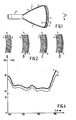
- Fig. 1 shows a cathode-ray tube 1 comprising an envelope 2 which comprises a neck portion 3, a flare portion 4 and a faceplate or viewing-screen portion 5.
- the neck portion 3 contains an electron gun, not shown, which emits electrons towards the screen. These electrons impinge on a fluorescent layer 6 provided on the inner surface 7 of the viewing screen.
- the visible light emitted by the fluorescent layer when an electron beam is incident on this layer is transmitted by the screen 5 and forms a picture which can be observed by a viewer W situated to the right of the outer surface 8 of the screen.
- Figs. 2a, 2b, 2c and 2d show different versions of the viewing screen in cross-section.
- Fig. 2a shows an "untreated" picture screen which has not been subjected to any anti-reflection treatment.
- This viewing screen has a reflectance of, for example, 4.2%.
- FIG. 2b shows a part of a viewing screen which is made anti-reflective by providing the outer surface 8 with a coating 9 which has a refractive index n c which is smaller than that of the glass.
- the reflectance can be reduced to a value well below the afore-mentioned 1.5% and can also be rendered less wavelength-dependent, which substantially reduces colour shading. All this can be achieved without an excessive reduction of the transmittance for the light produced by the fluorescent layer and the definition or resolving power of the picture.
- the outer surface of the screen is firstly roughened in a specific manner and subsequently an anti-reflective coating 9 is deposited on the roughened outer surface, for example by vapour-deposition.
- the surface profile is obtained mechanically, for example by treating the outer surface with silicon-carbide grains on a flexible polishing base. Roughening must be effected in such a manner that the resulting surface profile satisfies specific requirements. Preferably these requirements are defined by means of the known roughness parameters as specified in standards such as U.S.A. ANSIB 46.1 or U.K. Bs 1134.
- U.S.A. ANSIB 46.1 or U.K. Bs 1134.
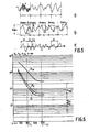
- R a , Rq, R tm and S m show how the relevant roughness parameters R a , Rq, R tm and S m are defined.
- the parameters R a and Rq, Rt m and Sm are defined with reference to Figs. 5a, 5b and 5c respectively, and are given by:
- the level I m has been selected in such a manner that of the total area between the roughness curve and the line l m the part above the level l m is equal to the part below l m .
- the sampling length L (Figs. 5a and 5b) is approximately 0.8 mm.
- the roughness of the outer surface of the viewing screen depends on the size of the grains used for roughening.
- the "Fachvic Elektrokorund und Siliziumkarbid Vietnamese Vietnamese Vietnamese soda.V.”, "F.E.P.A.” have defined a series of micrograins whose sizes range between 3 ⁇ m and 53 ⁇ m in accordance with the so-called F-series, as laid down in the "FEPA Mikrogrossen Standard für Schleifschkorn” (1965). This series ranges from F 230/50 with a grain size of 53.0 ⁇ 3.0 ⁇ m up to F 1200/3 with a grain size of 3 ⁇ 0.5 ⁇ m.
- FIG. 6 illustrates the variation of the parameters R a , Rq, R tm as a function of the grain size F thus defined on a logarithmic scale.
- R a , o , Rq, o and R tm , o are given in the left-hand part of Fig. 6.
- the roughness parameters for the outer surface of the viewing screen must satisfy the following requirements:
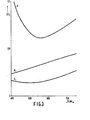
- the reflectance varies in accordance with the curve C shown in Fig. 3.
- the reflectance is now reduced to a low level: over the entire range of relevant wavelengths the reflectance R does not exceed 0.5%, whilst for a specific wavelength R it is even 0.3%.
- the wavelength-dependence is reduced substantially: the curve C is substantially flatter than the curve A.
- the scattering of light is substantially stronger for smaller wavelengths, the blue portion of the light spectrum, than for the higher wavelengths, the red portion of the light spectrum, so that the total reflectance becomes more insensitive to colour and colour shading is almost eliminated, no colour change being perceptible when the angle at which the viewed looks at the picture is varied.
- Fig. 4. shows the transmittance as a function of the wavelength for viewing screens treated in different manners.
- Curve D applies to a non-roughened viewing screen without anti-reflective coating.
- This screen has a transmittance of the order of 65%.
- the transmittance T of the screen decreases to a value which is of the order of 4% smaller, as illustrated by curve B.
- Ambient light is scattered and reflected at two locations by the viewing screen in accordance with the invention, namely at the transition from air to the coating 9 and at the transition from the coating 9 to the screen glass.
- the ambient light behaves as coherent light.
- the ambient light reflected at the transition from air to the coating 9 is reflected in phase opposition to the ambient light reflected at the transition from the coating 9 to the screen glass.
- the light which is reflected and scattered towards the viewer may be eliminated by destructive interference.
- Fig. 2d shows a small part of such a viewing screen in a cross-sectional view.
- the glass may be weakened as a result of roughening.
- the glass may be reinforced chemically before the anti-reflective coating is applied.
- the roughened surface may be brought into contact with a salt solution. This enables an exchange of Na + ions of the glass with metal ions, specifically K + ions, of the solution.
- the screen thus treated has an edge portion on the outer surface which is under stress, which portion via a neutral stress-free zone changes into an area under tensile stress. This results in a substantial reinforcement of the glass.
- European Patent Application No. 0.057.952 in which a reinforced glass mould is described.
- the outer surface of the picture screen i.e. the top coating
- magnesium-fluoride is somewhat sensitive to moisture and a layer of this material which has been vapour-deposited on the customary manner is not very hard. In normal vapour-deposition of an organic substances the vapour-deposition flow is directed at an acute angle with the surface to which the layer is to be applied. However, if magnesium-fluoride is vapour-deposited at an angle of 90° or an angle which deviates only slightly therefrom, a hard top-coating is obtained which is highly moisture-proof.
- This vapour-deposition may be applied both to a hot viewing screen, i.e. one heated to approximately 300°C, and to a cold viewing screen, which is at room temperature.
- a layer of magnesium-fluoride which has been vapour-deposited on a hot screen has slightly better properties than the same layer deposited on a cold viewing screen.
- vapour deposition on a cold screen is advantageous from the point of view of manufacturing technology.
- vapour-deposition on a cold viewing screen the roughened outer surface of the viewing screen is subjected to a glow-discharge in, for example, argon, gas for at least 15 minutes prior to vapour-deposition, so that the screen is chemically activated to ensure a correct adhesion between the screen and the coating 9.
- a hot screen is already activated in the intended sense and requires no additional treatment prior to vapour-deposition.
- the invention has been described for a television picture tube but may also be applied to other display systems using a transmissive viewing screen in which the picture to be displayed is situated close to the viewing screen.
Landscapes
- Physics & Mathematics (AREA)
- Chemical & Material Sciences (AREA)
- Inorganic Chemistry (AREA)
- General Physics & Mathematics (AREA)
- Optics & Photonics (AREA)
- Engineering & Computer Science (AREA)
- Multimedia (AREA)
- Signal Processing (AREA)
- Vessels, Lead-In Wires, Accessory Apparatuses For Cathode-Ray Tubes (AREA)
- Overhead Projectors And Projection Screens (AREA)
- Devices For Indicating Variable Information By Combining Individual Elements (AREA)
- Manufacture Of Electron Tubes, Discharge Lamp Vessels, Lead-In Wires, And The Like (AREA)
- Formation Of Various Coating Films On Cathode Ray Tubes And Lamps (AREA)
- Pharmaceuticals Containing Other Organic And Inorganic Compounds (AREA)
- Management, Administration, Business Operations System, And Electronic Commerce (AREA)
- Surface Treatment Of Optical Elements (AREA)
- Transforming Electric Information Into Light Information (AREA)
- Electrochromic Elements, Electrophoresis, Or Variable Reflection Or Absorption Elements (AREA)
Claims (9)
paramètres qui sont définis dans le American National Standard ANSI-B 46.1, chapter C3.
paramètres qui sont définis dans American National Standard ANSI-B 46.1, chapitre C3.
Priority Applications (1)
| Application Number | Priority Date | Filing Date | Title |
|---|---|---|---|
| AT84200996T ATE30985T1 (de) | 1983-07-11 | 1984-07-10 | Verfahren zum verringern der reflexionen in einem durchsichtigen bildschirm und bildschirm mit verringerter reflexion. |
Applications Claiming Priority (2)
| Application Number | Priority Date | Filing Date | Title |
|---|---|---|---|
| NL8302460 | 1983-07-11 | ||
| NL8302460A NL8302460A (nl) | 1983-07-11 | 1983-07-11 | Werkwijze voor het verminderen van de reflectie van een doorzichtig beeldscherm en beeldscherm met verminderde reflectie. |
Publications (2)
| Publication Number | Publication Date |
|---|---|
| EP0131341A1 EP0131341A1 (fr) | 1985-01-16 |
| EP0131341B1 true EP0131341B1 (fr) | 1987-11-19 |
Family
ID=19842141
Family Applications (1)
| Application Number | Title | Priority Date | Filing Date |
|---|---|---|---|
| EP84200996A Expired EP0131341B1 (fr) | 1983-07-11 | 1984-07-10 | Méthode de réduction des réflexions dans un écran transparent de visualisation et écran à réflexions réduites |
Country Status (12)
| Country | Link |
|---|---|
| US (1) | US4731558A (fr) |
| EP (1) | EP0131341B1 (fr) |
| JP (1) | JPH0679468B2 (fr) |
| KR (1) | KR920003717B1 (fr) |
| AT (1) | ATE30985T1 (fr) |
| BR (1) | BR8403407A (fr) |
| CA (1) | CA1229122A (fr) |
| DE (1) | DE3467660D1 (fr) |
| FI (1) | FI77128C (fr) |
| NL (1) | NL8302460A (fr) |
| PL (1) | PL248669A1 (fr) |
| YU (1) | YU119884A (fr) |
Families Citing this family (26)
| Publication number | Priority date | Publication date | Assignee | Title |
|---|---|---|---|---|
| NL8600184A (nl) * | 1986-01-28 | 1987-08-17 | Philips Nv | Doorzichtprojektiesysteem. |
| US4736743A (en) * | 1986-05-12 | 1988-04-12 | Surgical Laser Technology, Inc. | Vaporization contact laser probe |
| JPH058622Y2 (fr) * | 1986-07-31 | 1993-03-03 | ||
| GB8621468D0 (en) * | 1986-09-05 | 1986-10-15 | Philips Nv | Display device |
| US4884006A (en) * | 1986-12-30 | 1989-11-28 | Zenith Electronics Corporation | Inner surface specular reflection suppression in flat CRT faceplate |
| NL8700135A (nl) | 1987-01-21 | 1988-08-16 | Philips Nv | Doorzichtprojektiescherm en doorzichtprojektiesysteem voorzien van een dergelijk scherm. |
| LU86925A1 (fr) * | 1987-06-19 | 1989-03-08 | Glaverbel | Article en verre transmettant la lumiere et presentant une faible reflexion speculaire |
| JPH01117682U (fr) * | 1988-02-02 | 1989-08-09 | ||
| JPH01319232A (ja) * | 1988-06-17 | 1989-12-25 | Mitsubishi Electric Corp | 防眩処理形陰極線管 |
| EP0386235B1 (fr) * | 1988-08-08 | 1994-10-26 | NIPPON ELECTRIC GLASS COMPANY, Limited | Panneau pour tube cathodique |
| US4972117A (en) * | 1989-01-17 | 1990-11-20 | Zenith Electronics Corporation | Sparkle suppression displays |
| JPH05113505A (ja) * | 1991-10-22 | 1993-05-07 | Mitsubishi Electric Corp | 低反射膜付陰極線管およびその製造方法 |
| JP3355654B2 (ja) * | 1992-04-06 | 2002-12-09 | 松下電器産業株式会社 | 画像表示装置およびその製造方法 |
| US5455966A (en) * | 1992-12-03 | 1995-10-03 | U.S. Philips Corporation | Method of manufacturing a display window for a cathode ray tube and a cathode ray tube |
| JPH08138581A (ja) * | 1994-09-16 | 1996-05-31 | Toshiba Corp | 反射防止型陰極線管およびその製造方法 |
| JP3206713B2 (ja) * | 1995-10-27 | 2001-09-10 | 株式会社巴川製紙所 | 防眩材料及びそれを使用した偏光フィルム |
| TW337055B (en) * | 1996-03-29 | 1998-07-21 | Toshiba Co Ltd | EL screen packing film and the manufacturing method, the EL screen and the LCD module |
| US6250070B1 (en) * | 2000-05-09 | 2001-06-26 | Hughes Electronics Corporation | Ion thruster with ion-extraction grids having compound contour shapes |
| JP2003536216A (ja) * | 2000-06-07 | 2003-12-02 | コーニンクレッカ フィリップス エレクトロニクス エヌ ヴィ | 高圧放電ランプ |
| HUP0400039A3 (en) * | 2001-03-08 | 2004-10-28 | Boehringer Ingelheim Ca Ltd | Hcv polymerase inhibitor assay |
| JP3674849B2 (ja) * | 2001-11-15 | 2005-07-27 | 財団法人新産業創造研究機構 | 高効率ディスプレイ前面パネル |
| KR20050099260A (ko) * | 2004-04-09 | 2005-10-13 | 삼성전자주식회사 | 플라즈마 디스플레이 패널 |
| JP2007258672A (ja) * | 2006-02-22 | 2007-10-04 | Sharp Corp | 発光ダイオード及びその製造方法 |
| US7647881B2 (en) * | 2007-05-09 | 2010-01-19 | Visteon Global Technologies | Dimensional enhancement lens |
| CN103492336B (zh) * | 2011-04-15 | 2015-09-30 | 旭硝子株式会社 | 防反射性玻璃基体 |
| WO2021021436A1 (fr) * | 2019-07-30 | 2021-02-04 | Corning Incorporated | Procédés de revêtement d'un substrat avec du fluorure de magnésium par dépôt de couche atomique |
Family Cites Families (10)
| Publication number | Priority date | Publication date | Assignee | Title |
|---|---|---|---|---|
| US2044350A (en) * | 1934-04-13 | 1936-06-16 | Electrons Inc | Gaseous discharge tube and method of manufacture |
| US2612611A (en) * | 1950-06-23 | 1952-09-30 | Rauland Corp | Cathode-ray tube |
| FR1105039A (fr) * | 1954-05-26 | 1955-11-25 | American Optical Corp | Tube à rayons cathodiques |
| US3504212A (en) * | 1967-03-20 | 1970-03-31 | Westinghouse Electric Corp | High contrast display device incorporating a light absorption and scattering layer |
| NL6817661A (fr) * | 1968-12-10 | 1970-06-12 | ||
| JPS5171063A (ja) * | 1974-12-16 | 1976-06-19 | New Nippon Electric Co | Inkyokusenkan |
| JPS5293267A (en) * | 1976-01-30 | 1977-08-05 | Fujitsu Ltd | Reflection-proof film forming method for cathode-ray tube |
| JPS5313349A (en) * | 1976-07-22 | 1978-02-06 | Nec Home Electronics Ltd | Nonreflective cathode ray tube |
| JPS54129873A (en) * | 1978-03-31 | 1979-10-08 | Hitachi Ltd | Braun tube |
| US4410310A (en) * | 1981-04-23 | 1983-10-18 | Rca Corporation | Degassing a CRT with modified RF heating of the mount assembly thereof |
-
1983
- 1983-07-11 NL NL8302460A patent/NL8302460A/nl not_active Application Discontinuation
-
1984
- 1984-07-05 CA CA000458187A patent/CA1229122A/fr not_active Expired
- 1984-07-06 FI FI842727A patent/FI77128C/fi not_active IP Right Cessation
- 1984-07-09 YU YU01198/84A patent/YU119884A/xx unknown
- 1984-07-09 BR BR8403407A patent/BR8403407A/pt not_active IP Right Cessation
- 1984-07-10 DE DE8484200996T patent/DE3467660D1/de not_active Expired
- 1984-07-10 AT AT84200996T patent/ATE30985T1/de active
- 1984-07-10 EP EP84200996A patent/EP0131341B1/fr not_active Expired
- 1984-07-10 KR KR1019840004004A patent/KR920003717B1/ko not_active Expired
- 1984-07-11 PL PL24866984A patent/PL248669A1/xx unknown
- 1984-07-11 JP JP59142476A patent/JPH0679468B2/ja not_active Expired - Lifetime
-
1986
- 1986-11-03 US US06/926,820 patent/US4731558A/en not_active Expired - Fee Related
Also Published As
| Publication number | Publication date |
|---|---|
| US4731558A (en) | 1988-03-15 |
| KR850000870A (ko) | 1985-03-09 |
| FI77128C (fi) | 1989-01-10 |
| DE3467660D1 (en) | 1987-12-23 |
| PL248669A1 (en) | 1985-04-09 |
| NL8302460A (nl) | 1985-02-01 |
| FI842727A0 (fi) | 1984-07-06 |
| JPS6039744A (ja) | 1985-03-01 |
| FI77128B (fi) | 1988-09-30 |
| EP0131341A1 (fr) | 1985-01-16 |
| CA1229122A (fr) | 1987-11-10 |
| FI842727L (fi) | 1985-01-12 |
| KR920003717B1 (ko) | 1992-05-09 |
| JPH0679468B2 (ja) | 1994-10-05 |
| BR8403407A (pt) | 1985-06-18 |
| YU119884A (en) | 1988-02-29 |
| ATE30985T1 (de) | 1987-12-15 |
Similar Documents
| Publication | Publication Date | Title |
|---|---|---|
| US4731558A (en) | Method of reducing the reflectance of a transparent viewing screen and viewing screen with reduced reflectance | |
| US4798994A (en) | Low reflectance display device | |
| EP1490715B1 (fr) | Miroir de surface a revetement cda | |
| US4804883A (en) | Front attachment for CRT. E.G. for a monitor or video tube | |
| US4310783A (en) | Cathode ray tube face plate construction for suppressing the halo having a low reflection and method | |
| CA2150081A1 (fr) | Filtre electroconducteur accentuant les contrastes | |
| US5910333A (en) | Phosphor particle with antireflection coating | |
| US4132919A (en) | Absorbing inhomogeneous film for high contrast display devices | |
| EP0632294A1 (fr) | Miroirs | |
| US3504212A (en) | High contrast display device incorporating a light absorption and scattering layer | |
| US4540914A (en) | Absorbing graded nitride film for high contrast display devices | |
| US4310784A (en) | Cathode ray tube face plate construction for suppressing the halo and method | |
| US4465337A (en) | Reduced reflectivity member and ion implantation method of fabrication | |
| US5022726A (en) | Magnesium film reflectors | |
| IE57107B1 (en) | Rear-view mirror for vehicles,particularly motor vehicles,having a coating on the rear face | |
| CA2364533A1 (fr) | Couvercle pour source lumineuse | |
| JPH11171596A (ja) | 反射防止膜 | |
| US2918670A (en) | Luminescent presentation apparatus | |
| EP1184879A1 (fr) | Film conducteur a base de nitrures, procede de fabrication correspondant et objet antireflet | |
| US6586871B1 (en) | CRT panel glass and production method thereof and CRT | |
| JPS585855B2 (ja) | 半反射ガラス | |
| US5223765A (en) | Device for the display or projection of images or similar information with coating of adamantane carbon | |
| RU2737824C1 (ru) | Дихроическое зеркало | |
| JP2006337770A (ja) | 表面鏡 | |
| JP2002231132A (ja) | Crt用パネルガラスおよびcrt、並びにそれらの製造方法 |
Legal Events
| Date | Code | Title | Description |
|---|---|---|---|
| PUAI | Public reference made under article 153(3) epc to a published international application that has entered the european phase |
Free format text: ORIGINAL CODE: 0009012 |
|
| AK | Designated contracting states |
Designated state(s): AT DE FR GB IT |
|
| 17P | Request for examination filed |
Effective date: 19850311 |
|
| 17Q | First examination report despatched |
Effective date: 19860324 |
|
| GRAA | (expected) grant |
Free format text: ORIGINAL CODE: 0009210 |
|
| AK | Designated contracting states |
Kind code of ref document: B1 Designated state(s): AT DE FR GB IT |
|
| REF | Corresponds to: |
Ref document number: 30985 Country of ref document: AT Date of ref document: 19871215 Kind code of ref document: T |
|
| REF | Corresponds to: |
Ref document number: 3467660 Country of ref document: DE Date of ref document: 19871223 |
|
| ITF | It: translation for a ep patent filed | ||
| ET | Fr: translation filed | ||
| PLBE | No opposition filed within time limit |
Free format text: ORIGINAL CODE: 0009261 |
|
| STAA | Information on the status of an ep patent application or granted ep patent |
Free format text: STATUS: NO OPPOSITION FILED WITHIN TIME LIMIT |
|
| 26N | No opposition filed | ||
| PG25 | Lapsed in a contracting state [announced via postgrant information from national office to epo] |
Ref country code: AT Effective date: 19890710 |
|
| ITTA | It: last paid annual fee | ||
| ITPR | It: changes in ownership of a european patent |
Owner name: CAMBIO RAGIONE SOCIALE;PHILIPS ELECTRONICS N.V. |
|
| REG | Reference to a national code |
Ref country code: FR Ref legal event code: CD |
|
| PGFP | Annual fee paid to national office [announced via postgrant information from national office to epo] |
Ref country code: GB Payment date: 19970701 Year of fee payment: 14 |
|
| PGFP | Annual fee paid to national office [announced via postgrant information from national office to epo] |
Ref country code: FR Payment date: 19970722 Year of fee payment: 14 |
|
| PGFP | Annual fee paid to national office [announced via postgrant information from national office to epo] |
Ref country code: DE Payment date: 19970917 Year of fee payment: 14 |
|
| PG25 | Lapsed in a contracting state [announced via postgrant information from national office to epo] |
Ref country code: GB Free format text: LAPSE BECAUSE OF NON-PAYMENT OF DUE FEES Effective date: 19980710 |
|
| REG | Reference to a national code |
Ref country code: FR Ref legal event code: CD |
|
| GBPC | Gb: european patent ceased through non-payment of renewal fee |
Effective date: 19980710 |
|
| PG25 | Lapsed in a contracting state [announced via postgrant information from national office to epo] |
Ref country code: FR Free format text: LAPSE BECAUSE OF NON-PAYMENT OF DUE FEES Effective date: 19990331 |
|
| PG25 | Lapsed in a contracting state [announced via postgrant information from national office to epo] |
Ref country code: DE Free format text: LAPSE BECAUSE OF NON-PAYMENT OF DUE FEES Effective date: 19990501 |
|
| REG | Reference to a national code |
Ref country code: FR Ref legal event code: ST |