EP0132314A2 - Circuit mémoire avec fenêtre d'adressage - Google Patents
Circuit mémoire avec fenêtre d'adressage Download PDFInfo
- Publication number
- EP0132314A2 EP0132314A2 EP84304325A EP84304325A EP0132314A2 EP 0132314 A2 EP0132314 A2 EP 0132314A2 EP 84304325 A EP84304325 A EP 84304325A EP 84304325 A EP84304325 A EP 84304325A EP 0132314 A2 EP0132314 A2 EP 0132314A2
- Authority
- EP
- European Patent Office
- Prior art keywords
- window
- register
- circuit
- addressable memory
- input
- Prior art date
- Legal status (The legal status is an assumption and is not a legal conclusion. Google has not performed a legal analysis and makes no representation as to the accuracy of the status listed.)
- Granted
Links
Images

Classifications
-
- G—PHYSICS
- G01—MEASURING; TESTING
- G01S—RADIO DIRECTION-FINDING; RADIO NAVIGATION; DETERMINING DISTANCE OR VELOCITY BY USE OF RADIO WAVES; LOCATING OR PRESENCE-DETECTING BY USE OF THE REFLECTION OR RERADIATION OF RADIO WAVES; ANALOGOUS ARRANGEMENTS USING OTHER WAVES
- G01S7/00—Details of systems according to groups G01S13/00, G01S15/00, G01S17/00
- G01S7/02—Details of systems according to groups G01S13/00, G01S15/00, G01S17/00 of systems according to group G01S13/00
- G01S7/021—Auxiliary means for detecting or identifying radar signals or the like, e.g. radar jamming signals
-
- G—PHYSICS
- G06—COMPUTING OR CALCULATING; COUNTING
- G06F—ELECTRIC DIGITAL DATA PROCESSING
- G06F7/00—Methods or arrangements for processing data by operating upon the order or content of the data handled
- G06F7/02—Comparing digital values
- G06F7/026—Magnitude comparison, i.e. determining the relative order of operands based on their numerical value, e.g. window comparator
Definitions
- the present invention relates generally to memory circuits, and more particularly, to special-purpose memory circuits used in digital signal processing systems.
- memory circuits There is a general class of computational problems in which numerical data must be sorted in accordance with its relationship to one or more sets of dimensional limits. It is with this class of problems that the present invention is concerned.
- Pattern recognition has many well known applications in both military and commercial areas.
- each received radar signal is preprocessed into digital fields that characterize and completely define the signal.
- the fields might contain such information as time of arrival, frequency, pulse amplitude, pulse width, angle of arrival, and so forth.
- there may be many such signals whose sources are known and are of no consequence to the purpose of the signal processing. Since the characteristics of these signals from known sources are also known, a first processing step is usually to filter out these known signals from the ones of more particular interest.
- This filtering step is analogous to finding the number of people in a selected age group in a particular region of the country, but in the radar example the specified items are discarded rather than further analyzed. Both applications, however, are examples of a processing step that might be described environmental filtering.
- the present invention resides in a memory circuit capable of high speed sorting of items of input data, based on the relationship of the data to stored upper and lower limits in multiple dimensions.
- the circuit simultaneously compares each input data item with multiple pairs of upper and lower limits, and provides an indication of whether or not the item falls within the limits.
- the window-addressable memory circuit of the invention comprises input ciruit means, for inputting data words having a plurality of data fields, memory means, for storing a plurality of sets of upper and lower limits, dual comparator means, for simultaneously comparing the stored plurality of upper and lower limits with each input data word, and output circuit means, for indicating whether any of the comparisons made in the dual comparator means resulted in a match.
- the circuit also includes means for specifying a plurality of fields in the input data words.
- the comparisons with upper and lower limits are performed on the fields separately, but practically at the same time, and there has to be a match in all fields in order to produce a match signal for that particular set of limits.
- the input data item must fall between the specified limits for all fields or dimensions of the data item.
- a plurality of such comparisons is performed simultaneously for different sets of upper and lower limits, and the output provided comprises a plurality of match signals, one for each set of upper and lower limits in use, and a composite match signal indicating whether there was a match for any one or more of the sets of limits.
- the circuit of the invention also includes means for selecting the field lengths within the input data words, and means for selectively enabling and disabling the individual "windows" of upper and lower limits. Also included are means for loading and unloading the memory means with upper and lower limit data, and means for segmenting the input data words so that less than a full-length word may be optionally input.
- the circuit is intended for implementation in monolithic form, although is not necessarily limited to this form.
- the memory means holds as many as eight sets of upper and lower limits, but multiple circuits can be cascaded to allow for the use of multiples of eight windows to be simultaneously applied to the same data.
- the present invention represents a significant advance in the field of digital signal processing.
- the invention provides a high speed circuit for sorting data in accordance with the relationship between multiple fields or dimensions of the data and corresponding multiple sets of upper and lower limits.
- the present invention is concerned with digital memory circuits used in the processing of statistical and other data. It is often desired to sort or filter data in relation to windows of upper and lower limits in multiple dimensions. Although this sorting process can be performed in a digital computer, the computer processing time may be too great for some applications in which a real-time response is needed.
- such data can be compared simultaneously with multiple sets of upper and lower limits, in a special-purpose circuit that can perform the comparisons at very high speed.
- the data fallfng within the prescribed window limits in all dimensions will be retained for further processing.
- the data falling within the prescribed window limits will be discarded, while the remaining data will be retained for further processing.
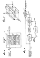
- FIG. 1 shows the basic function of the window-addressable memory circuit, which is indicated by reference numeral 10.
- the circuit receives a sequence of 48-bit input words. It will be understood, of course, that the size of the input word is not a limiting factor.
- each input word is compared with up to eight sets of upper and lower limits stored in the circuit. Match signals are provided on eight output lines 16, to indicate whether the input word fell within the eight sets of upper and lower limits. A single composite match signal is also provided, on line 18, to indicate whether a match occurred for any of the eight sets of limits.
- the circuit 10 also includes a field-length control register 20, and a window enable register 22.
- the field-length control register 20 defines how the 48-bit data word is divided into logical fields of data. In the illustrative embodiment, there may be as many as twelve fields of four bits each, or a smaller number of fields having multiples of four bits each.
- the field-length control register 20 defines the field boundaries within the data word and within the corresponding upper and lower limits.
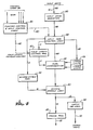
- FIG. 4 shows the window-addressable memory (WAM) circuit in more detail.
- the principal components are a dual comparator 24, a random access memory 25 for the storage of sets of upper and lower limits, input data registers 26, input register control logic 28, window enable logic 30, match OR logic 32, a match register 34, and function control and input control logic 36.
- Data is input over the lines 12 to the input register 26, and is input to the dual comparator 24 through the input register control logic 28, which also functions to transmit upper and lower limit data to the memory 25, and to transmit new data to the field length control register 20 and the window enable register 22.
- Selection of the circuits various functions is effected by means of a plurality of control lines 38, to be described in detail, and the function control and input control logic 36, as indicated by the broken lines 40 and 42.
- the dual comparator 24 compares the input data word with each set of upper and lower limits. If any field of the data word does not fall within the upper and lower limits of that field, no match is found as a result of the comparison.
- the function of the field-length control register 20 is to define the fields of the data word. Each bit of the field-length control register corresponds to a boundary between two adjacent four-bit segments of the data word. If the register bit is a one, this indicates a continuation of a data field from one four-bit segment to the next. If the register bit is a zero, this indicates a data field boundary. The bit position to the right of the boundary is treated as the most significant bit of its data field, and the bit to the left of the boundary is treated as the least significant bit of the next data field.
- the window enable register 22 is a mask register that permits a user of the circuit to examine or ignore the results of each of the eight window comparisons.
- the window enable logic 30 is basically a plurality of AND gates. One input of each AND gate is derived from the match outputs, and the other is derived from the window enable register.
- the dual comparator 24 is constructed in the presently preferred embodiment of the invention as a plurality of pairs of subtractor circuits, each of which has as one input the input data word.
- the other inputs of each pair of subtractor circuits are the upper and lower limits, respectively, of a set of window data taken from the memory 25.
- An appropriate signal from one subtractor of a pair of such circuits indicates that the data is less than or equal to the upper limit, and a signal from the other subtractor in the pair indicates that the data is greater than or equal to the lower limit.
- the two signals are ANDed together to produce a match signal for that particular window.
- the same function is performed simultaneously for the other seven windows, and the eight match signals are next presented to the window enable logic 30, and then to the match register 34.
- the data fields in the input words are variable, and may be redefined by changing the field-length control register 20.
- the effect of the register 20 is to treat certain designated bits of the data word and the upper and lower limit words as though they were the most significant bits of a field.
- the result of a subtraction is positive only if the subtraction of each of the separate fields yields a positive result. In other words, if one field is out of limits, the entire data word is said to be out of limits.
- FIG. 2 shows in graphical form the application of the circuit to the processing of data relating to coordinates in three spatial dimensions, X, Y and Z.
- the upper and lower limits in the X direction are X and X L , respectively, while those in the Y and Z directions are Y U , Y L r Z U ' and Z L .
- a match signal will be obtained on all three bits of line 18, corresponding to the three spatial dimensions only for coordinate sets falling inside the rectangular box indicated at 50 in FIG. 2. These coordinates may be either discarded or further processed, depending on the requirements of the particular problem.
- the WAM circuit is not limited to the processing of data in the form of spatial dimensions.
- the "dimensional" properties of the data may be representative of physical variables, such as frequency, direction, amplitude, or time; demographic variables such as age, geographical area, religion, occupation, or income; or any other types of variables.
- FIG. 3 illustrates another application of the WAM circuit, for the sorting of radar signal pulses in accordance with their physical characteristics.
- data is being received over line 52 at a very high rate, such as two megapulses per second.
- Each pulse is initially processed into digital form and is defined by a total of 72 bits of data, of which 24 bits are used to store the time of arrival of the pulse. The remaining 48 bits completely characterize the pulse, and therefore its source.
- it is desired to focus attention on those pulses whose characteristics are not known in advance. There will be some pulses in the stream that are derived from known sources, and the processing of which may not be important to the problem. Accordingly, it is desired to eliminate those known pulses as identified by their characteristics or "dimensions," a task for which the WAM circuit is extremely well suited.
- the inputs on line 52 are passed through a switch chip 54, which functions as a multiplexer, and thence to a WAM chip 56 for processing in the manner described above.
- the 48 bits of data is divided into a total of six fields, including the band, frequency, pulse amplitude, pulse width, angle of arrival, and a set of flag bits.
- Operation of the WAM chip 56 and the switch chip 54 is directed by a control chip 58, which is responsible for storing in the WAM chip 56 upper and lower limits relating to known radar sources. The upper and lower limits are transmitted over line 60 to the switch chip 54, and thence to the WAM chip 56.
- control signals are transmitted over line 64 to the WAM chip 56, to instruct it to receive and store limit data rather than data to be compared.
- a match signal is generated on line 66, a match has been found with respect to one of the windows of limits.
- the signal on line 66 is used to inhibit the storing of information relating to the currently processed pulse in a buffer memory chip 68, to which the input data on line 52 is also connected.
- the output from the buffer memory chip 68, on line 70 represents only the pulses whose characteristics did not fit any of the plurality of stored limits in the WAM chip 56.
- the information on line 70 can then be subject to further processing, such as counting in a histogrammer circuit (not shown).
- the WAM chip 56 performs a very high speed filtering step on the incoming data in real time, something that could not be achieved using conventional processing methods without a significant sacrifice in the speed of response.
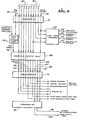
- FIG. 5 is a block diagram of the entire WAM circuit, including more than the principal components shown in FIG. 4.
- the function control and input control logic 36 includes three registers 74, 75 and 76, the function of which will be further explained in relation to FIG. 6.
- the control lines 38 include a single instruction inhibit (II) line 78, three input data register control lines 80, six function select lines 82, and five input select lines 84, all of which are input to the first register 74.
- the control logic 36 functions as a timing sequencer, producing control signals on line 40 to control the input register 26, on line 42 to control loading of the field length control register 20 and the window enable register 22, and on line 86 to control loading of the match register 34.
- control logic 36 generates a control signal on line 88 to tri-state control logic 90.
- the latter controls a 48-bit tri-state output register 92, which receives inputs over lines 94 from the memory, and provides outputs over lines 96 to the data input lines 12.
- the data input lines are shown as divided into three segments of sixteen bits each.
- the tri-state output register 92 provides an output path from the memory 25, permitting a user of the circuit to read the upper and lower limits stored in the memory.
- Tri-state register devices are widely used in digital circuit design where external connections to a circuit are to serve two or more separate purposes, such as input and output, at different times.
- the tri-state output register 92 presents a high impedance to the input lines 12 when input data is impressed on the input lines, but presents a relatively low-impedance path when output data is being transferred from the memory 25 to the input lines 12a, 12b and 12c.
- each circuit may be assigned a chip address, as stored in a chip address register 100.
- An output enable compare circuit 102 compares this local chip address with a chip address selected by means of a set of output selection lines 104, which are coupled to a register 106 and thence to the output enable compare circuit.
- a match signal is transmitted over line 108 to a transparent flip-flop 110, and thence to a tri-state control circuit 112, which controls a tri-state match buffer 114.
- the match buffer 114 is coupled to receive the contents of the match register 34, and when appropriately instructed by the tri-state control circut 112, to couple the contents of the match register out onto output lines 116.
- the circuit has to be properly addressed by the output select signals on lines 104 before the tri-state buffer 114 will couple the match signals onto the output lines 116.
- the two tri-state control circuits 90 and 112 include as inputs a reset signal designated RS/ (shown in the drawing as RS), an enable signal line EN1 and an auxiliary control line AUX.
- the EN1 and AUX signals are used only in a special maintenance mode of operation, which does not relate to the invention.
- the reset signal RS/ forces the tri-state outputs to a high impedance and generates a delayed reset signal, which is applied to the window enable register 22, to the control register 74 in the control circuitry 36, to the match register 34, and to the tri-state output register 92.
- Register 74 part of register 76, output select register 106, flip-flop 110, and the match register 34, are all designated as transparent registers in FIG. 5.
- This aspect of the circuit design is of no direct consequence to the invention, but rather relates to detailed timing considerations important to users of the circuit.
- These registers are transparent in a timing sense, since they interpose practically no timing delay between their inputs and outputs.
- each of the five transparent registers may be selectively rendered non-transparent by separate control signals (not shown), available to the user of the circuit.
- This transparency control may be desirable in certain applications of the WAM circuit. Basically, register transparency control is an operational option that is closely related to the specific application of the circuit.
- Control lines 80, 82 and 84, and the instruction inhibit line 78 together provide inputs to register 76, also referred to as control register #1.
- the outputs from register 74 are variously coupled to a load instruction decoder 120, to operation decode logic 122, and to an input address comparator 124.
- the input register control signals derived from the control lines 80, designated ICO, IC1 and IC2 are directed to the load instruction decoder 120, together with the instruction inhibit signal (II), and the decoder generates a segment MUX control signal on line 126 and three segment enable signals on lines 128, 129 and 130.
- II instruction inhibit signal
- the segment MUX control signal on line 126 is derived directly from the ICl control signal, since it will be noted that IC1 is a logical "1" only when segment #2 or segment #3 is being loaded separately.
- IC1 is a logical "1" only when segment #2 or segment #3 is being loaded separately.
- the input data is applied to the sixteen input lines 12a (FIG. 5) for segment #1.
- the data is also applied to the segment #1 input lines 12a, but the data must be directed to the appropriate input register segment.
- multiplexers 132 and 133 which are normally switched to transmit data from input lines 12b and 12c, respectively, to the corresponding input register stages.
- a logical "1" control signal is applied to the multiplexers, over line 126 from the load instruction decoder 120, the multiplexers are switched to accept data from the segment #1 input lines 12a.
- the input selection control lines 84 are transmitted through the first register 74 to the input chip address comparator 124, which serves the same function for input as the address comparator 102 (FIG. 5) serves for output. If the address coded on the input selection lines 84 matches the address in the chip address register 100, a chip enable signal is generated on line 134 from the input chip comparator 124 to the operation decode logic 122.
- the operation decode logic 122 receives as inputs the six function selection lines 82, designated IFO through IF5, together with the chip enable line 134, the instruction inhibit line 78, and the input selection line 80 designated IC2.
- the operation decode logic 122 generates control signal outputs in accordance with the functions set forth in TABLE II below.
- the operation decode logic 122 generates ten output signals for transmission to control register #2 (75), including four lines 136 that are derived directly from function control lines IFO - IF3, and one line 138 that is derived directly from the instruction inhibit line 78.
- the other five outputs of the operation decode logic 122 are a read memory line 140 (READEN), a write memory line 142 (WRITEN), a field length load line 144 (FLTH L D), a window enable load line 146 (WENLD), and a compare line 148 (COMPAR). After all of these signals have been passed through the second register 75, they are used as control signals in the following manner.
- the memory control signals are the read memory line 140 and the write memory line 142 to convey the memory function to be performed, and lines 136 to convey the memory address.
- the line derived from function input IF3 indicates whether a memory address containing an upper limit or a lower limit is to be addressed, and the lines derived from IFO - IF2 indicate the window number (0 through 7) being addressed.
- Loading of the field length control register 20 is initiated by means of a signal on control line 144, and loading of the window enable register is initiated by means of a signal on control line 146.
- ADREN is the address enable signal supplied on line 134.
- WRTAND, WRTOR, OTHR, OTHRAND, and OTHROR are intermediate signals used as set forth in the logic equations.
- the present invention represents a significant advance in the field of memory circuits used in certain types of signal processing systems.
- the invention provides a high speed circuit for filtering data in relation to prescribed windows of upper and lower limits.
- the data may include a plurality of fields or dimensions, and the comparisons are simultaneously performed for a plurality of limit windows.
Landscapes
- Engineering & Computer Science (AREA)
- Physics & Mathematics (AREA)
- General Physics & Mathematics (AREA)
- Radar, Positioning & Navigation (AREA)
- Remote Sensing (AREA)
- Theoretical Computer Science (AREA)
- Mathematical Optimization (AREA)
- Mathematical Analysis (AREA)
- Computational Mathematics (AREA)
- Pure & Applied Mathematics (AREA)
- General Engineering & Computer Science (AREA)
- Computer Networks & Wireless Communication (AREA)
- Logic Circuits (AREA)
- Information Retrieval, Db Structures And Fs Structures Therefor (AREA)
- Radar Systems Or Details Thereof (AREA)
- Image Processing (AREA)
Applications Claiming Priority (2)
| Application Number | Priority Date | Filing Date | Title |
|---|---|---|---|
| US06/517,083 US4627024A (en) | 1983-07-21 | 1983-07-21 | Window-addressable memory circuit |
| US517083 | 1990-05-01 |
Publications (3)
| Publication Number | Publication Date |
|---|---|
| EP0132314A2 true EP0132314A2 (fr) | 1985-01-30 |
| EP0132314A3 EP0132314A3 (en) | 1989-02-22 |
| EP0132314B1 EP0132314B1 (fr) | 1991-07-24 |
Family
ID=24058283
Family Applications (1)
| Application Number | Title | Priority Date | Filing Date |
|---|---|---|---|
| EP84304325A Expired EP0132314B1 (fr) | 1983-07-21 | 1984-06-26 | Circuit mémoire avec fenêtre d'adressage |
Country Status (4)
| Country | Link |
|---|---|
| US (1) | US4627024A (fr) |
| EP (1) | EP0132314B1 (fr) |
| JP (1) | JPS6043741A (fr) |
| DE (1) | DE3484830D1 (fr) |
Families Citing this family (13)
| Publication number | Priority date | Publication date | Assignee | Title |
|---|---|---|---|---|
| US5050067A (en) * | 1987-08-20 | 1991-09-17 | Davin Computer Corporation | Multiple sliding register stacks in a computer |
| US5053991A (en) * | 1989-10-06 | 1991-10-01 | Sanders Associates, Inc. | Content-addressable memory with soft-match capability |
| US5125098A (en) * | 1989-10-06 | 1992-06-23 | Sanders Associates, Inc. | Finite state-machine employing a content-addressable memory |
| US5572682A (en) * | 1992-04-03 | 1996-11-05 | Cyrix Corporation | Control logic for a sequential data buffer using byte read-enable lines to define and shift the access window |
| JPH06119146A (ja) * | 1992-10-07 | 1994-04-28 | Nippon Motorola Ltd | データのソート回路 |
| US5477227A (en) * | 1993-11-19 | 1995-12-19 | Trw Inc. | Advanced parameter encoder with environmental filter capability |
| JP2677202B2 (ja) * | 1994-08-12 | 1997-11-17 | 日本電気株式会社 | マイクロプロセッサ |
| US7133400B1 (en) | 1998-08-07 | 2006-11-07 | Intel Corporation | System and method for filtering data |
| US7333484B2 (en) * | 1998-08-07 | 2008-02-19 | Intel Corporation | Services processor having a packet editing unit |
| US6721842B2 (en) | 1999-01-29 | 2004-04-13 | Intel Corporation | Boundary addressable memory |
| US6625440B1 (en) | 2000-01-31 | 2003-09-23 | Trw Inc. | Drum memory controller |
| US6252790B1 (en) * | 2000-10-16 | 2001-06-26 | Nicholas Shectman | Large-capacity content addressable memory with sorted insertion |
| WO2002043069A2 (fr) * | 2000-11-07 | 2002-05-30 | Fast-Chip, Inc. | Memoire adressable par la limite |
Family Cites Families (6)
| Publication number | Priority date | Publication date | Assignee | Title |
|---|---|---|---|---|
| US3845465A (en) * | 1973-01-12 | 1974-10-29 | Us Air Force | Associative storage apparatus for comparing between specified limits |
| US3931612A (en) * | 1974-05-10 | 1976-01-06 | Triad Systems Corporation | Sort apparatus and data processing system |
| JPS5127036A (ja) * | 1974-08-30 | 1976-03-06 | Yokogawa Electric Works Ltd | Deijitarumaruchireberukonpareeta |
| IT1131177B (it) * | 1980-05-14 | 1986-06-18 | Consiglio Nazionale Ricerche | Comparator a banda programmabile,multicanale,per unita' cardiochirurgiche |
| NL8005136A (nl) * | 1980-09-12 | 1982-04-01 | Philips Nv | Inrichting voor het associatief zoeken in een sekwentiele informatiestroom die is opgebouwd uit informatievakken. |
| US4475237A (en) * | 1981-11-27 | 1984-10-02 | Tektronix, Inc. | Programmable range recognizer for a logic analyzer |
-
1983
- 1983-07-21 US US06/517,083 patent/US4627024A/en not_active Expired - Lifetime
-
1984
- 1984-06-26 DE DE8484304325T patent/DE3484830D1/de not_active Expired - Fee Related
- 1984-06-26 EP EP84304325A patent/EP0132314B1/fr not_active Expired
- 1984-07-20 JP JP59151145A patent/JPS6043741A/ja active Pending
Also Published As
| Publication number | Publication date |
|---|---|
| EP0132314B1 (fr) | 1991-07-24 |
| EP0132314A3 (en) | 1989-02-22 |
| JPS6043741A (ja) | 1985-03-08 |
| DE3484830D1 (de) | 1991-08-29 |
| US4627024A (en) | 1986-12-02 |
Similar Documents
| Publication | Publication Date | Title |
|---|---|---|
| US4559618A (en) | Content-addressable memory module with associative clear | |
| EP0132314B1 (fr) | Circuit mémoire avec fenêtre d'adressage | |
| US5010516A (en) | Content addressable memory | |
| US4314356A (en) | High-speed term searcher | |
| US4628483A (en) | One level sorting network | |
| US4607331A (en) | Method and apparatus for implementing an algorithm associated with stored information | |
| US5303200A (en) | N-dimensional multi-port memory | |
| US4597009A (en) | Method and circuit arrangement for video-rapid determination of the median of an evaluation window | |
| US3845465A (en) | Associative storage apparatus for comparing between specified limits | |
| JPS58121460A (ja) | プログラム可能な範囲識別器 | |
| US3109162A (en) | Data boundary cross-over and/or advance data access system | |
| US5440714A (en) | Method and system configuration for simplifying the decoding system for access to an register file with overlapping windows | |
| US3289171A (en) | Push-down list storage using delay line | |
| US5659755A (en) | Method and system in a data processing system for efficiently compressing data using a sorting network | |
| EP0167959A2 (fr) | Traitement pour registres de vecteur de calculateur | |
| US4327407A (en) | Data driven processor | |
| RU2067317C1 (ru) | Устройство сортировки символов | |
| US4764895A (en) | Data processor for changing the sequential format of inputted records | |
| US5450526A (en) | Fuzzy neuron having pixel address memory | |
| JPS62256035A (ja) | 可変のデ−タバス幅をもつプログラム装置におけるプログラム制御のシフト機構 | |
| US4584664A (en) | Sorting apparatus | |
| JPS63187334A (ja) | 文字列パタ−ンマツチング装置 | |
| US3594731A (en) | Information processing system | |
| SU1683034A1 (ru) | Устройство дл анализа параметров графа | |
| US20080079483A1 (en) | Circuit and device for processing digital data |
Legal Events
| Date | Code | Title | Description |
|---|---|---|---|
| PUAI | Public reference made under article 153(3) epc to a published international application that has entered the european phase |
Free format text: ORIGINAL CODE: 0009012 |
|
| AK | Designated contracting states |
Designated state(s): BE DE FR GB NL |
|
| PUAL | Search report despatched |
Free format text: ORIGINAL CODE: 0009013 |
|
| AK | Designated contracting states |
Kind code of ref document: A3 Designated state(s): BE DE FR GB NL |
|
| 17P | Request for examination filed |
Effective date: 19890710 |
|
| 17Q | First examination report despatched |
Effective date: 19900327 |
|
| GRAA | (expected) grant |
Free format text: ORIGINAL CODE: 0009210 |
|
| AK | Designated contracting states |
Kind code of ref document: B1 Designated state(s): BE DE FR GB NL |
|
| REF | Corresponds to: |
Ref document number: 3484830 Country of ref document: DE Date of ref document: 19910829 |
|
| ET | Fr: translation filed | ||
| PLBE | No opposition filed within time limit |
Free format text: ORIGINAL CODE: 0009261 |
|
| STAA | Information on the status of an ep patent application or granted ep patent |
Free format text: STATUS: NO OPPOSITION FILED WITHIN TIME LIMIT |
|
| 26N | No opposition filed | ||
| PGFP | Annual fee paid to national office [announced via postgrant information from national office to epo] |
Ref country code: NL Payment date: 19970331 Year of fee payment: 14 |
|
| PGFP | Annual fee paid to national office [announced via postgrant information from national office to epo] |
Ref country code: GB Payment date: 19970506 Year of fee payment: 14 |
|
| PGFP | Annual fee paid to national office [announced via postgrant information from national office to epo] |
Ref country code: FR Payment date: 19970610 Year of fee payment: 14 |
|
| PGFP | Annual fee paid to national office [announced via postgrant information from national office to epo] |
Ref country code: DE Payment date: 19970627 Year of fee payment: 14 |
|
| PGFP | Annual fee paid to national office [announced via postgrant information from national office to epo] |
Ref country code: BE Payment date: 19970708 Year of fee payment: 14 |
|
| PG25 | Lapsed in a contracting state [announced via postgrant information from national office to epo] |
Ref country code: GB Free format text: LAPSE BECAUSE OF NON-PAYMENT OF DUE FEES Effective date: 19980626 |
|
| PG25 | Lapsed in a contracting state [announced via postgrant information from national office to epo] |
Ref country code: BE Free format text: LAPSE BECAUSE OF NON-PAYMENT OF DUE FEES Effective date: 19980630 |
|
| BERE | Be: lapsed |
Owner name: TRW INC. Effective date: 19980630 |
|
| PG25 | Lapsed in a contracting state [announced via postgrant information from national office to epo] |
Ref country code: NL Free format text: LAPSE BECAUSE OF NON-PAYMENT OF DUE FEES Effective date: 19990101 |
|
| GBPC | Gb: european patent ceased through non-payment of renewal fee |
Effective date: 19980626 |
|
| PG25 | Lapsed in a contracting state [announced via postgrant information from national office to epo] |
Ref country code: FR Free format text: LAPSE BECAUSE OF NON-PAYMENT OF DUE FEES Effective date: 19990226 |
|
| NLV4 | Nl: lapsed or anulled due to non-payment of the annual fee |
Effective date: 19990101 |
|
| PG25 | Lapsed in a contracting state [announced via postgrant information from national office to epo] |
Ref country code: DE Free format text: LAPSE BECAUSE OF NON-PAYMENT OF DUE FEES Effective date: 19990401 |
|
| REG | Reference to a national code |
Ref country code: FR Ref legal event code: ST |