EP0133010A2 - Circuit céramique multicouche - Google Patents
Circuit céramique multicouche Download PDFInfo
- Publication number
- EP0133010A2 EP0133010A2 EP84305023A EP84305023A EP0133010A2 EP 0133010 A2 EP0133010 A2 EP 0133010A2 EP 84305023 A EP84305023 A EP 84305023A EP 84305023 A EP84305023 A EP 84305023A EP 0133010 A2 EP0133010 A2 EP 0133010A2
- Authority
- EP
- European Patent Office
- Prior art keywords
- ceramic
- circuit board
- thermal expansion
- amount
- layers
- Prior art date
- Legal status (The legal status is an assumption and is not a legal conclusion. Google has not performed a legal analysis and makes no representation as to the accuracy of the status listed.)
- Granted
Links
Images
Classifications
-
- H—ELECTRICITY
- H10—SEMICONDUCTOR DEVICES; ELECTRIC SOLID-STATE DEVICES NOT OTHERWISE PROVIDED FOR
- H10W—GENERIC PACKAGES, INTERCONNECTIONS, CONNECTORS OR OTHER CONSTRUCTIONAL DETAILS OF DEVICES COVERED BY CLASS H10
- H10W70/00—Package substrates; Interposers; Redistribution layers [RDL]
- H10W70/60—Insulating or insulated package substrates; Interposers; Redistribution layers
- H10W70/611—Insulating or insulated package substrates; Interposers; Redistribution layers for connecting multiple chips together
-
- H—ELECTRICITY
- H05—ELECTRIC TECHNIQUES NOT OTHERWISE PROVIDED FOR
- H05K—PRINTED CIRCUITS; CASINGS OR CONSTRUCTIONAL DETAILS OF ELECTRIC APPARATUS; MANUFACTURE OF ASSEMBLAGES OF ELECTRICAL COMPONENTS
- H05K1/00—Printed circuits
- H05K1/02—Details
- H05K1/03—Use of materials for the substrate
- H05K1/0306—Inorganic insulating substrates, e.g. ceramic, glass
-
- H—ELECTRICITY
- H10—SEMICONDUCTOR DEVICES; ELECTRIC SOLID-STATE DEVICES NOT OTHERWISE PROVIDED FOR
- H10W—GENERIC PACKAGES, INTERCONNECTIONS, CONNECTORS OR OTHER CONSTRUCTIONAL DETAILS OF DEVICES COVERED BY CLASS H10
- H10W70/00—Package substrates; Interposers; Redistribution layers [RDL]
- H10W70/60—Insulating or insulated package substrates; Interposers; Redistribution layers
- H10W70/62—Insulating or insulated package substrates; Interposers; Redistribution layers characterised by their interconnections
- H10W70/63—Vias, e.g. via plugs
- H10W70/635—Through-vias
-
- H—ELECTRICITY
- H10—SEMICONDUCTOR DEVICES; ELECTRIC SOLID-STATE DEVICES NOT OTHERWISE PROVIDED FOR
- H10W—GENERIC PACKAGES, INTERCONNECTIONS, CONNECTORS OR OTHER CONSTRUCTIONAL DETAILS OF DEVICES COVERED BY CLASS H10
- H10W70/00—Package substrates; Interposers; Redistribution layers [RDL]
- H10W70/60—Insulating or insulated package substrates; Interposers; Redistribution layers
- H10W70/62—Insulating or insulated package substrates; Interposers; Redistribution layers characterised by their interconnections
- H10W70/66—Conductive materials thereof
- H10W70/666—Organic materials or pastes
-
- H—ELECTRICITY
- H10—SEMICONDUCTOR DEVICES; ELECTRIC SOLID-STATE DEVICES NOT OTHERWISE PROVIDED FOR
- H10W—GENERIC PACKAGES, INTERCONNECTIONS, CONNECTORS OR OTHER CONSTRUCTIONAL DETAILS OF DEVICES COVERED BY CLASS H10
- H10W70/00—Package substrates; Interposers; Redistribution layers [RDL]
- H10W70/60—Insulating or insulated package substrates; Interposers; Redistribution layers
- H10W70/67—Insulating or insulated package substrates; Interposers; Redistribution layers characterised by their insulating layers or insulating parts
- H10W70/69—Insulating materials thereof
-
- H—ELECTRICITY
- H10—SEMICONDUCTOR DEVICES; ELECTRIC SOLID-STATE DEVICES NOT OTHERWISE PROVIDED FOR
- H10W—GENERIC PACKAGES, INTERCONNECTIONS, CONNECTORS OR OTHER CONSTRUCTIONAL DETAILS OF DEVICES COVERED BY CLASS H10
- H10W70/00—Package substrates; Interposers; Redistribution layers [RDL]
- H10W70/60—Insulating or insulated package substrates; Interposers; Redistribution layers
- H10W70/62—Insulating or insulated package substrates; Interposers; Redistribution layers characterised by their interconnections
- H10W70/63—Vias, e.g. via plugs
-
- H—ELECTRICITY
- H10—SEMICONDUCTOR DEVICES; ELECTRIC SOLID-STATE DEVICES NOT OTHERWISE PROVIDED FOR
- H10W—GENERIC PACKAGES, INTERCONNECTIONS, CONNECTORS OR OTHER CONSTRUCTIONAL DETAILS OF DEVICES COVERED BY CLASS H10
- H10W90/00—Package configurations
- H10W90/701—Package configurations characterised by the relative positions of pads or connectors relative to package parts
- H10W90/721—Package configurations characterised by the relative positions of pads or connectors relative to package parts of bump connectors
- H10W90/724—Package configurations characterised by the relative positions of pads or connectors relative to package parts of bump connectors between a chip and a stacked insulating package substrate, interposer or RDL
Definitions
- the present invention relates to a multilayered ceramic circuit board for example a multilayered printed ceramic circuit board on which LSIs can be directly mounted.
- Ceramic circuit boards are often used for the mounting of semiconductor elements, in line with the trend towards constructing electronic circuits in a highly integrated form.
- Alumina porcelain has hitherto been chosen for the production of ceramic boards, in view of its thermal conductivity, mechanical strength and electrical insulation.
- alumina ceramic materials have a dielectric constant (herein also referred to as specific inductive capacity) as large as about 9, which means that signal transmission within electronic circuits is delayed, which is a disadvantage when transmitting signals at high speeds.
- Alumina ceramic materials are fired at temperatures of as high as 1500° to 1650°C and only metal materials of a high melting point, such as tungsten, molybdenum or the like, can be used for forming wiring circuits simultaneously with the firing of the ceramic material.
- Tungsten and molybdenum are materials that are difficult to bake, and exhibit electrical resistances of as much as 5.2 and 5.5 microohms.cm at room temperature.
- the wiring When circuits are formed at a high density, the wiring must have reduced width, so that the electrical resistance thereof per unit length increases. Accordingly, the signal transmission speed is reduced by voltage drop.
- Another problem which arises is the formation of cracks at the edges of through-holes in the ceramic layers, there being electrically conductive material in the through-holes making inter-layer connections between the conductive layers.
- An object of the invention is to provide a multi-layer ceramic circuit board in which at least one of the dielectric constant of the ceramic material and the resistance of the conductive material is reduced.
- the glass composition preferably consists essentially of SiO 2 in an amount of 10 to 80%, B 2 0 3 in an amount of 15 to 65%, Al 2 O 3 in an amount of 3 to 27%, up to 15% of MgO, up to 35% of BaO, up to 45% of AlPO 4 , up to 18% of MgF 2 , up to 10% of K 2 0, up to 5% of Na 2 0, and up to 17% of Bi 2 O 3 .
- the SiO 2 -containing additive preferably has a linear thermal expansion coefficient of less than 100 x 10 -7 /°C over the temperature range of 25 to 850°C.
- the glass composition consists essentially of SiO 2 in an amount of 30 to 50%, B 2 0 3 in an amount of 20 to 50%, Al 2 O 3 in an amount of 5 to 15%, up to 10% of MgO, up to 20% of BaO, up to 30% of AlPO 4 , up to 10% of MgF 2 , up to 10% of K 2 0, up to 5% of Na 2 0, and up to 10% of Bi203, and has a softening point lower than 850°C.
- the Si0 2 -containing additive may be a member selected from the group consisting of quartz (100 x 10 -7 /°C), quartz glass (0.5 x 10 -7 /°C), cristobalite (100 x 10 -7 /°C), tridymite (80 x 10 -7 /°C) and mixtures thereof.
- quartz 100 x 10 -7 /°C
- quartz glass 0.5 x 10 -7 /°C
- cristobalite 100 x 10 -7 /°C
- tridymite 80 x 10 -7 /°C
- the glass composition may alternatively consist essentially of 30 to 60% of SiO 2 , 10 to 40% of B 2 O 3 , 5 to 15% of A1 2 0 3' 2 to 15% of BaO and/or MgO, and up to 5% of Na 2 0 and/or K 2 0.
- the conductive layers may have a coefficient of thermal expansion larger than that of the ceramic material, but the materials for the conductor and ceramic material are preferably selected so that the difference between the coefficients of thermal expansion of the conductor and the ceramic material is less than 100 x 10 -7 /°C.
- the metal is preferably selected from the group consisting of silver, copper, gold, their alloys and mixtures thereof.
- the glass composition in said conductive layers is preferably the same glass compositions as that of the ceramic layers.
- Known examples of materials with an excellent electric conductivity include silver (1.6'microohms.cm), copper (1.7 microohms.cm) and gold (2.2 microohms.cm). These materials melt at 961°C, 1083°C and 1063°C, respectively.
- To use these conductors on a ceramic multilayer circuit board it is necessary to select a ceramic material that can be sintered at a temperature lower than these melting points. If fired at a temperature higher than the melting point of the electrically conductive material, the conductors formed by a printing method would melt, which would result in line breakages or short circuits.
- Silver, copper and gold have small resistivities, but have coefficients of thermal expansion of as much as 193 x 10 -7 /°C, 173 x 10 7 /°C, and 150 x 10 -7 /°C, respectively.
- the coefficient of thermal expansion of the ceramic material should not differ much from the coefficient of thermal expansion (35 x 10 -7 /°C) of silicon, so that reliability of the connection portions is not lost. It is therefore desired that the ceramic material has a coefficient of thermal expansion which is less than the coefficient of thermal expansion (about 70 x 10 -7 /°C) of alumina which is currently used in practice. On the other hand, if the ceramic material has a coefficient of thermal expansion which is less than 70 x 10 /°C, the difference between it and the coefficient of thermal expansion of silver, copper or gold increases, and cracks may develop in the boundaries between through holes and the ceramic material.
- the electrically conductive material should have a small resistivity and should preferably have a coefficient of thermal expansion such that cracks do not develop in the boundaries between through holes and the ceramic material.
- conductors must be fomed in through holes so as to connect the wiring conductors through the ceramic materials that act as insulators. It is possible to reduce the pitch of the through holes in order to prevent the occurrence of cracks in the boundaries between the through holes and the ceramic material, when using silver, copper or gold, which have small resistivities but large coefficients of thermal expansion, as the electrically conductive material.
- the electrically conductive material contains silver, copper or gold
- the ceramic material has a coefficient of thermal expansion of less than 70 x 10 -7 /°C
- arcuate cracks develop in the boundaries between through holes and the ceramic material when the through holes have a diameter of 0.1 mm and a pitch of more than 0.5 mm, in contrast with the use of an alumina'ceramic material and tungsten, or an alumina ceramic material and molybdenum. It has, however, been discovered that no cracks develop when the pitch of the through holes is reduced to less than 0.5 mm.
- an electrically conductive material composed chiefly of a metal which has a low resistivity, such as copper, gold or the like, and which also contains a material with a small coefficient of thermal expansion as a filler, in order to reduce the coefficient of thermal expansion of the resultant electrically conductive material.
- the ceramic material has a coefficient of thermal expansion of less than 70 x 10 -7 /°C
- the difference between the coefficient of thermal expansion of the ceramic material and the coefficient of thermal expansion of the electrically conductive material could exceed 100 x 10 -7 /°C.
- cracks may develop to some extent in the boundaries between through holes and the ceramic material. It has, however, been found that no cracks develop when the difference between the coefficients of thermal expansion of the ceramic material and the electrically conductive material is less than 100 x 10 -7 /°C.
- Thermal stresses caused by differences in coefficients of thermal expansion were analyzed by a finite element method, using a system in which through holes were provided in a ceramic material at equal distances. It was found that when the coefficient of thermal expansion of the ceramic material is less than the coefficient of thermal expansion of the electrically conductive material, tensile stresses are exerted in the radial direction from the centers of the through holes, and compressive stresses are exerted in the circumferential direction thereof. It is known that ceramic materials are generally strong against compressive stresses but are weak against tensile stresses. In this case, the stresses act to separate the boundaries between the through holes and the ceramic material.
- the pitch of the through holes should be reduced when the coefficient of thermal expansion of the ceramic material is less than that of the electrically conductive material. That is, by forming the wiring at a high density, the generation of thermal stresses can be reduced and the development of cracks restrained.
- the present invention can provide a multilayered ceramic circuit board in which the electrically conductive material has a coefficient of thermal expansion larger than that of the ceramic material, the materials for the conductor and ceramic material being selected so that the difference between their respective coefficients of thermal expansion is less than 100 x 10 -7 /°C.
- the pitch of through holes is less than 0.5 mm.
- the electrically conductive material is preferably silver, copper, gold, or an alloy which contains at least one of these elements, and the ceramic material preferably has a coefficient of thermal expansion of between 30 to 70 x 10 -7 /°C.
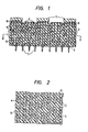
- Figs. 1 and 2 show one form of multilayered ceramic circuit board to which the invention can be applied.
- Semiconductor devices 1 e.g. chips
- Between the ceramic layers 5 are wiring layers 4 of electrically conductive material and connections between the layers 4 are made by electrically conductive material 3 in through-holes in the ceramic layers.
- terminals 2 At the top face of the board, there are terminals 2 and at the bottom face there are pin terminals 7. Examples of the Invention
- the conductive material used in the through-holes was the same as that used for the conductive layers between the ceramic layers.
- the materials other than Si0 2 and B 2 0 3 constitute the refractory additive.
- Silicon oxide exists in a variety of forms such as quartz, quartz glass, cristobalite, tridymite, etc., which have different coefficients of thermal expansion. A desired coefficient of thermal expansion can be obtained by using these various silicon oxides as fillers.
- each of starting ceramic materials 100 parts were mixed at the mixture ratios shown in Table 2 in a ball mill for 24 hours.
- 6.0 parts of a polyvinyl butyral resin, 2.4 parts dioctyl phthalate, 23.0 parts trichloroethylene, 9.0 parts perchloroethylene and 6.0 parts butyl alcohol were introduced into the ball mill and mixed therein for 10 hours.
- the mixtures assumed a slurry form.
- the slurries were continuously applied at a thickness of 0.25 mm onto polyester film using a doctor blade.
- the sheets were heated at a maximum temperature of 120°C so that solvents therein were evaporated. Green sheets were thus obtained, which were cut into pieces of a predetermined shape.
- Through holes 0.1 mm in diameter were formed by a punching method at a pitch of between 0.2 and 2.0 mm, and the through holes were filled with an electrically conductive paste of silver by a printing method to form conductors for connecting wiring between the layers.
- Wiring conductors of a predetermined pattern were printed onto the surfaces of the sheets.
- Six green sheets on which silver conductors had been printed were stacked with the aid of guide holes, and were stuck together at 120°C under a pressure of 10 kg/ cm 2 .
- Ceramic circuit boards with six electrically conductive layers was obtained through these steps. Since silver was used as the conductor for the circuit boards, the resistivity of the wiring was 0.4 ohm/cm at a wiring width of 80 um.
- Through holes 0.1 mm in diameter were formed by a punching method at a pitch of between 0.2 and2.0 mm, and six green sheets on which an electrically conductive paste of copper had bean formed were stacked with the aid of guide holes, and were stuck together at 120°C under a pressure of 15 kg/cm 2 .
- the stacked green sheets were introduced into a furnace and were fired in a nitrogen atmosphere containing between 3 to 7 % hydrogen. Small amounts of water vapor were introduced into the atmosphere to promote the thermal decomposition of the organic binders. Firing was effected at the same temperatures as in Example 1.
- Circuit boards with six electrically conductive layers were obtained through these steps. Since copper was used as the conductor for the circuit boards, the resistivity of the wiring was 0.4 ohm/cm at a wiring width of 80 um.
- each of starting ceramic materials 100 parts were mixed at the mixture ratios shown in Table 3 in a ball mill for 24 hours.
- 6.0 parts of a polyvinyl butyral resin, 2.4 parts dioctyl phthalate, 23.0 parts trichloroethylene, 9.0 parts perchloroethylene and 6.0 parts butyl alcohol were introduced into the ball mill and mixed therein for 10 hours.
- the mixtures assumed a slurry form.
- the slurries were continuously applied at a thickness of 0.25 mm onto polyester film using a doctor blade.
- the sheets were heated at a maximum temperature of 120°C to evaporate the solvents therein. Green sheets were thus obtained, which were cut into pieces of a predetermined shape. Predetermined through holes were formed therein by a punching method.
- Electrically conductive pastes were prepared at the mixture ratios shown in Table 4, and con- ' ductors were formed in the through holes by a printing method, to connect the wiring layers. Wiring conductors of a predetermined pattern were also printed on the surfaces of the sheets. Six green sheets on which conductors of silver- or gold-types had been printed were stacked with the aid of guide holes, and were stuck together at 120°C under a pressure of 10 kg/ cm 2 .
- the stacked green sheets were introduced into a furnace and were fired in an atmosphere of air.
- the firing was effected at the sintering temperature shown in Table 3 for about 30 minutes.
- Ceramic circuit boards with six electrically conductive layers were obtained through these steps.
- each starting ceramic materials 100 parts were mixed at the mixture ratios shown in Table 3 in a ball mill for 24 hours, in the same manner as in Example 1. 5.9 parts methacrylic acid resin, 2.4 parts dioctyl phthalate, 23.0 parts ethyl acetate, 9.0 parts butyl acetate and 6.0 parts butyl alcohol were introduced into the ball mill and mixed therein for 10 hours. The mixtures assumed a slurry form. The slurries were continuously applied at a thickness of 0.25 mm onto polyester film using a doctor blade. The sheets were heated at a maximum temperature of 120°C to evaporate the solvents therein.
- Green sheets were thus formed, which were then cut into pieces of a predetermined shape, and predetermined through holes were formed therein by a punching method. Electrically conductive pastes were prepared at the mixture ratios shown in Table 5, and conductors were formed in the through holes by a printing method to connect the wiring layers. Wiring conductors of a predetermined pattern were also printed onto the surfaces of the sheets. Six green sheets on which conductors of the copper-type had been printed were stacked with the aid of guide holes, and were stuck together at 120°C under a pressure of 10 kg/cm 2 .
- the stacked green sheets were introduced into a furnace and were fired in a nitrogen atmosphere containing between 3 to 7 % hydrogen. Small quantities of water vapor were introduced into the atmosphere to promote the thermal decomposition of the organic binders. The firing was effected at the same temperatures as in Example 1.
- Ceramic circuit boards were obtained according to the same procedure as that of Example 3, with the exception of using, as the electrically conductive material, a silver-type paste containing the same low-temperature softening glass as that used for the ceramic starting material.
- Table 6 shows the blending ratios of the electrically conductive materials, the coefficients of thermal expansion, and the presence of cracks in the vicinities of the through holes when these electrically conductive materials were used.
- Ceramic circuit boards were obtained according to the same procedure as that of Example 4, with the exception of using, as the electrically conductive material, a copper-type paste containing the same low-temperature softening glass as was used for the ceramic starting materials.
- Table 7 shows the blending ratios of the electrically conductive materials, the coefficients of thermal expansion, and the presence of cracks in the vicinities of the through holes when these electrically conductive materials were used.
Landscapes
- Engineering & Computer Science (AREA)
- Chemical & Material Sciences (AREA)
- Ceramic Engineering (AREA)
- Inorganic Chemistry (AREA)
- Microelectronics & Electronic Packaging (AREA)
- Production Of Multi-Layered Print Wiring Board (AREA)
- Laminated Bodies (AREA)
Applications Claiming Priority (2)
| Application Number | Priority Date | Filing Date | Title |
|---|---|---|---|
| JP135882/83 | 1983-07-27 | ||
| JP58135882A JPS6028296A (ja) | 1983-07-27 | 1983-07-27 | セラミツク多層配線回路板 |
Publications (3)
| Publication Number | Publication Date |
|---|---|
| EP0133010A2 true EP0133010A2 (fr) | 1985-02-13 |
| EP0133010A3 EP0133010A3 (en) | 1986-06-25 |
| EP0133010B1 EP0133010B1 (fr) | 1990-09-26 |
Family
ID=15161979
Family Applications (1)
| Application Number | Title | Priority Date | Filing Date |
|---|---|---|---|
| EP84305023A Expired EP0133010B1 (fr) | 1983-07-27 | 1984-07-24 | Circuit céramique multicouche |
Country Status (4)
| Country | Link |
|---|---|
| US (1) | US4598167A (fr) |
| EP (1) | EP0133010B1 (fr) |
| JP (1) | JPS6028296A (fr) |
| DE (1) | DE3483292D1 (fr) |
Cited By (6)
| Publication number | Priority date | Publication date | Assignee | Title |
|---|---|---|---|---|
| EP0207466A3 (fr) * | 1985-06-27 | 1987-08-12 | Kabushiki Kaisha Toshiba | Substrat pour circuits |
| FR2604716A1 (fr) * | 1986-10-02 | 1988-04-08 | Rca Corp | Encres de remplissage d'interconnexions entre couches en cuivre en film epais |
| EP0262975A3 (fr) * | 1986-10-02 | 1989-02-08 | General Electric Company | Encres pour conducteur cuivré à film épais |
| EP0245770A3 (en) * | 1986-05-14 | 1989-03-15 | Narumi China Corporation | Multilayer ceramic substrate with circuit patterns |
| EP0569799A3 (fr) * | 1992-05-14 | 1994-01-05 | Matsushita Electric Industrial Co Ltd | |
| EP1083600A3 (fr) * | 1994-08-19 | 2005-05-25 | Hitachi, Ltd. | Substrat de circuit multi-couche |
Families Citing this family (34)
| Publication number | Priority date | Publication date | Assignee | Title |
|---|---|---|---|---|
| US4632846A (en) * | 1984-09-17 | 1986-12-30 | Kyocera Corporation | Process for preparation of glazed ceramic substrate and glazing composition used therefor |
| JPH0634452B2 (ja) * | 1985-08-05 | 1994-05-02 | 株式会社日立製作所 | セラミツクス回路基板 |
| JPS6273799A (ja) * | 1985-09-27 | 1987-04-04 | 日本電気株式会社 | 多層セラミツク配線基板 |
| JPS62287658A (ja) * | 1986-06-06 | 1987-12-14 | Hitachi Ltd | セラミックス多層回路板 |
| JPH0797703B2 (ja) * | 1986-09-04 | 1995-10-18 | 松下電器産業株式会社 | セラミツク多層基板 |
| WO1988003087A1 (fr) * | 1986-10-30 | 1988-05-05 | Olin Corporation | Composite en ceramique-verre-metal |
| US5024883A (en) * | 1986-10-30 | 1991-06-18 | Olin Corporation | Electronic packaging of components incorporating a ceramic-glass-metal composite |
| US4883778A (en) * | 1986-10-30 | 1989-11-28 | Olin Corporation | Products formed of a ceramic-glass-metal composite |
| US4882212A (en) * | 1986-10-30 | 1989-11-21 | Olin Corporation | Electronic packaging of components incorporating a ceramic-glass-metal composite |
| JPH01248593A (ja) * | 1988-03-30 | 1989-10-04 | Ngk Insulators Ltd | セラミック多層配線基板 |
| US4910643A (en) * | 1988-06-06 | 1990-03-20 | General Electric Company | Thick film, multi-layer, ceramic interconnected circuit board |
| US5164342A (en) * | 1988-10-14 | 1992-11-17 | Ferro Corporation | Low dielectric, low temperature fired glass ceramics |
| US5258335A (en) * | 1988-10-14 | 1993-11-02 | Ferro Corporation | Low dielectric, low temperature fired glass ceramics |
| US5071794A (en) * | 1989-08-04 | 1991-12-10 | Ferro Corporation | Porous dielectric compositions |
| JPH05500584A (ja) * | 1989-09-25 | 1993-02-04 | イー・アイ・デユポン・ドウ・ヌムール・アンド・カンパニー | 改良された複合誘電体 |
| JPH0461293A (ja) * | 1990-06-29 | 1992-02-27 | Toshiba Corp | 回路基板及びその製造方法 |
| US5283104A (en) * | 1991-03-20 | 1994-02-01 | International Business Machines Corporation | Via paste compositions and use thereof to form conductive vias in circuitized ceramic substrates |
| US5264399A (en) * | 1992-04-28 | 1993-11-23 | International Business Machines Corporation | Ceramic composite body |
| US5342999A (en) * | 1992-12-21 | 1994-08-30 | Motorola, Inc. | Apparatus for adapting semiconductor die pads and method therefor |
| US5587885A (en) * | 1994-05-18 | 1996-12-24 | Dell Usa, L.P. | Mechanical printed circuit board/laminated multi chip module interconnect apparatus |
| US5400220A (en) * | 1994-05-18 | 1995-03-21 | Dell Usa, L.P. | Mechanical printed circuit board and ball grid array interconnect apparatus |
| US6323549B1 (en) * | 1996-08-29 | 2001-11-27 | L. Pierre deRochemont | Ceramic composite wiring structures for semiconductor devices and method of manufacture |
| JP2001507867A (ja) * | 1996-12-30 | 2001-06-12 | デロシェモント,エル.ピエール | 半導体装置用セラミックコンポジットワイヤ構造体及び製造方法 |
| US6162997A (en) * | 1997-06-03 | 2000-12-19 | International Business Machines Corporation | Circuit board with primary and secondary through holes |
| US7474536B2 (en) | 2000-10-27 | 2009-01-06 | Ridley Ray B | Audio sound quality enhancement apparatus and method |
| US7186461B2 (en) * | 2004-05-27 | 2007-03-06 | Delaware Capital Formation, Inc. | Glass-ceramic materials and electronic packages including same |
| US7387838B2 (en) * | 2004-05-27 | 2008-06-17 | Delaware Capital Formation, Inc. | Low loss glass-ceramic materials, method of making same and electronic packages including same |
| US7561436B2 (en) | 2005-06-06 | 2009-07-14 | Delphi Technologies, Inc. | Circuit assembly with surface-mount IC package and heat sink |
| WO2007122548A2 (fr) * | 2006-04-20 | 2007-11-01 | Nxp B.V. | Isolation thermique de dispositifs électroniques dans une embase pour applications d'éclairage à del |
| AT503706B1 (de) * | 2006-06-07 | 2011-07-15 | Mikroelektronik Ges Mit Beschraenkter Haftung Ab | Schaltungsträger |
| JP4935217B2 (ja) * | 2006-07-18 | 2012-05-23 | 富士通株式会社 | 多層配線基板 |
| JP2007173857A (ja) * | 2007-02-13 | 2007-07-05 | Kyocera Corp | 多層基板およびその製造方法 |
| US8904631B2 (en) | 2011-04-15 | 2014-12-09 | General Electric Company | Method of fabricating an interconnect device |
| EP2750141B1 (fr) | 2012-12-28 | 2018-02-07 | Heraeus Deutschland GmbH & Co. KG | Pâte électroconductrice comprenant des particules d'oxyde inorganiques grossières dans la préparation d'électrodes pour cellules solaires MWT |
Family Cites Families (19)
| Publication number | Priority date | Publication date | Assignee | Title |
|---|---|---|---|---|
| US3450545A (en) * | 1966-05-31 | 1969-06-17 | Du Pont | Noble metal metalizing compositions |
| US3762936A (en) * | 1967-07-31 | 1973-10-02 | Du Pont | Manufacture of borosilicate glass powder essentially free of alkali and alkaline earth metals |
| DE2218283A1 (de) * | 1971-04-24 | 1972-11-23 | N.V. Philips Gloeilampenfabrieken, Eindhoven (Niederlande) | Verfahren zur Herstellung eines Gemenges für ein Borsilikatglas |
| DE2306236C2 (de) * | 1973-02-08 | 1982-11-25 | Siemens AG, 1000 Berlin und 8000 München | Verfahren zur Herstellung von Schichtschaltungen mit leitenden Schichten auf beiden Seiten eines Keramiksubstrates |
| DE2517743C3 (de) * | 1975-04-22 | 1980-03-06 | Jenaer Glaswerk Schott & Gen., 6500 Mainz | Passivierender Schutzüberzug für Siliziumhalbleiterbauelemente |
| US4072771A (en) * | 1975-11-28 | 1978-02-07 | Bala Electronics Corporation | Copper thick film conductor |
| US4029605A (en) * | 1975-12-08 | 1977-06-14 | Hercules Incorporated | Metallizing compositions |
| US4109377A (en) * | 1976-02-03 | 1978-08-29 | International Business Machines Corporation | Method for preparing a multilayer ceramic |
| US4301324A (en) * | 1978-02-06 | 1981-11-17 | International Business Machines Corporation | Glass-ceramic structures and sintered multilayer substrates thereof with circuit patterns of gold, silver or copper |
| JPS5563900A (en) * | 1978-11-08 | 1980-05-14 | Fujitsu Ltd | Multilyaer ceramic circuit board |
| JPS55133597A (en) * | 1979-04-06 | 1980-10-17 | Hitachi Ltd | Multilayer circuit board |
| US4355114A (en) * | 1979-11-05 | 1982-10-19 | Rca Corporation | Partially devitrified porcelain containing BaO.2MgO.2SiO2 and 2MgO.B2 O3 crystalline phases obtained from alkali metal free divalent metal oxide borosilicate glass |
| US4256796A (en) * | 1979-11-05 | 1981-03-17 | Rca Corporation | Partially devitrified porcelain composition and articles prepared with same |
| JPS5729185U (fr) * | 1980-07-28 | 1982-02-16 | ||
| US4369254A (en) * | 1980-10-17 | 1983-01-18 | Rca Corporation | Crossover dielectric inks |
| GB2102026B (en) * | 1981-06-05 | 1985-07-10 | Matsushita Electric Industrial Co Ltd | Conductive pastes |
| US4415624A (en) * | 1981-07-06 | 1983-11-15 | Rca Corporation | Air-fireable thick film inks |
| JPS5817651A (ja) * | 1981-07-24 | 1983-02-01 | Hitachi Ltd | 多層回路板とその製造方法 |
| JPS5911700A (ja) * | 1982-07-12 | 1984-01-21 | 株式会社日立製作所 | セラミツク多層配線回路板 |
-
1983
- 1983-07-27 JP JP58135882A patent/JPS6028296A/ja active Granted
-
1984
- 1984-07-24 DE DE8484305023T patent/DE3483292D1/de not_active Expired - Lifetime
- 1984-07-24 EP EP84305023A patent/EP0133010B1/fr not_active Expired
- 1984-07-25 US US06/634,066 patent/US4598167A/en not_active Expired - Lifetime
Cited By (7)
| Publication number | Priority date | Publication date | Assignee | Title |
|---|---|---|---|---|
| EP0207466A3 (fr) * | 1985-06-27 | 1987-08-12 | Kabushiki Kaisha Toshiba | Substrat pour circuits |
| EP0245770A3 (en) * | 1986-05-14 | 1989-03-15 | Narumi China Corporation | Multilayer ceramic substrate with circuit patterns |
| FR2604716A1 (fr) * | 1986-10-02 | 1988-04-08 | Rca Corp | Encres de remplissage d'interconnexions entre couches en cuivre en film epais |
| EP0262975A3 (fr) * | 1986-10-02 | 1989-02-08 | General Electric Company | Encres pour conducteur cuivré à film épais |
| EP0569799A3 (fr) * | 1992-05-14 | 1994-01-05 | Matsushita Electric Industrial Co Ltd | |
| US5496619A (en) * | 1992-05-14 | 1996-03-05 | Matsushita Electric Industrial Co., Ltd. | Assembly formed from conductive paste and insulating paste |
| EP1083600A3 (fr) * | 1994-08-19 | 2005-05-25 | Hitachi, Ltd. | Substrat de circuit multi-couche |
Also Published As
| Publication number | Publication date |
|---|---|
| DE3483292D1 (de) | 1990-10-31 |
| US4598167A (en) | 1986-07-01 |
| JPS6028296A (ja) | 1985-02-13 |
| EP0133010A3 (en) | 1986-06-25 |
| EP0133010B1 (fr) | 1990-09-26 |
| JPH0326554B2 (fr) | 1991-04-11 |
Similar Documents
| Publication | Publication Date | Title |
|---|---|---|
| EP0133010A2 (fr) | Circuit céramique multicouche | |
| EP0131242B1 (fr) | Substrat céramique multi-couches et procédé pour sa fabrication | |
| EP0211619B1 (fr) | Plaquette de circuit céramique multicouche | |
| KR930000881B1 (ko) | 세라믹 다층 회로판 및 반도체 모듈 | |
| US5757611A (en) | Electronic package having buried passive components | |
| JPS6244879B2 (fr) | ||
| JPS599992A (ja) | 多層配線基板の製造方法 | |
| JP3528037B2 (ja) | ガラスセラミック基板の製造方法 | |
| EP0478971A2 (fr) | Composition diélectrique contenant de la cordiérite et du verre | |
| EP0532842A1 (fr) | Composition inorganique faiblement diélectrique pour un assemblage céramique multicouche | |
| EP0997941B1 (fr) | Pâte conductrice et substrat céramique imprimé | |
| EP0247617A2 (fr) | Substrat multi-couche en céramique ayant une configuration de circuits | |
| JPH025315B2 (fr) | ||
| JPH0816021B2 (ja) | 多層ガラスセラミック基板およびその製造方法 | |
| JP3093601B2 (ja) | セラミック回路基板 | |
| KR100744855B1 (ko) | 높은 열적 사이클 전도체 시스템 | |
| JPH06334351A (ja) | 導体ペーストおよびそれを用いたセラミック多層配線基板 | |
| JPH11284296A (ja) | 配線基板 | |
| JPH06120633A (ja) | セラミック配線基板 | |
| JP3426920B2 (ja) | 配線基板 | |
| JP3164664B2 (ja) | 多層回路基板 | |
| JP3905991B2 (ja) | ガラスセラミック配線基板 | |
| JP3176258B2 (ja) | 多層配線基板 | |
| JP2002015620A (ja) | 導体組成物およびこれを用いた配線基板 | |
| JPH0470124B2 (fr) |
Legal Events
| Date | Code | Title | Description |
|---|---|---|---|
| PUAI | Public reference made under article 153(3) epc to a published international application that has entered the european phase |
Free format text: ORIGINAL CODE: 0009012 |
|
| 17P | Request for examination filed |
Effective date: 19840828 |
|
| AK | Designated contracting states |
Designated state(s): DE FR GB |
|
| PUAL | Search report despatched |
Free format text: ORIGINAL CODE: 0009013 |
|
| AK | Designated contracting states |
Kind code of ref document: A3 Designated state(s): DE FR GB |
|
| 17Q | First examination report despatched |
Effective date: 19880812 |
|
| GRAA | (expected) grant |
Free format text: ORIGINAL CODE: 0009210 |
|
| AK | Designated contracting states |
Kind code of ref document: B1 Designated state(s): DE FR GB |
|
| REF | Corresponds to: |
Ref document number: 3483292 Country of ref document: DE Date of ref document: 19901031 |
|
| ET | Fr: translation filed | ||
| PLBE | No opposition filed within time limit |
Free format text: ORIGINAL CODE: 0009261 |
|
| STAA | Information on the status of an ep patent application or granted ep patent |
Free format text: STATUS: NO OPPOSITION FILED WITHIN TIME LIMIT |
|
| 26N | No opposition filed | ||
| PGFP | Annual fee paid to national office [announced via postgrant information from national office to epo] |
Ref country code: FR Payment date: 19980619 Year of fee payment: 15 |
|
| PGFP | Annual fee paid to national office [announced via postgrant information from national office to epo] |
Ref country code: GB Payment date: 19980624 Year of fee payment: 15 |
|
| PGFP | Annual fee paid to national office [announced via postgrant information from national office to epo] |
Ref country code: DE Payment date: 19980930 Year of fee payment: 15 |
|
| PG25 | Lapsed in a contracting state [announced via postgrant information from national office to epo] |
Ref country code: GB Free format text: LAPSE BECAUSE OF NON-PAYMENT OF DUE FEES Effective date: 19990724 |
|
| PG25 | Lapsed in a contracting state [announced via postgrant information from national office to epo] |
Ref country code: FR Free format text: THE PATENT HAS BEEN ANNULLED BY A DECISION OF A NATIONAL AUTHORITY Effective date: 19990731 |
|
| GBPC | Gb: european patent ceased through non-payment of renewal fee |
Effective date: 19990724 |
|
| PG25 | Lapsed in a contracting state [announced via postgrant information from national office to epo] |
Ref country code: DE Free format text: LAPSE BECAUSE OF NON-PAYMENT OF DUE FEES Effective date: 20000503 |
|
| REG | Reference to a national code |
Ref country code: FR Ref legal event code: ST |