EP0133080A1 - Frequenzunabhängiger Impedanzanpassungsvierpol und Wanderwellenverstärker der diesen verwendet - Google Patents
Frequenzunabhängiger Impedanzanpassungsvierpol und Wanderwellenverstärker der diesen verwendet Download PDFInfo
- Publication number
- EP0133080A1 EP0133080A1 EP84401410A EP84401410A EP0133080A1 EP 0133080 A1 EP0133080 A1 EP 0133080A1 EP 84401410 A EP84401410 A EP 84401410A EP 84401410 A EP84401410 A EP 84401410A EP 0133080 A1 EP0133080 A1 EP 0133080A1
- Authority
- EP
- European Patent Office
- Prior art keywords
- impedance
- circuit
- quadrupole
- value
- input
- Prior art date
- Legal status (The legal status is an assumption and is not a legal conclusion. Google has not performed a legal analysis and makes no representation as to the accuracy of the status listed.)
- Granted
Links
- 230000006978 adaptation Effects 0.000 claims abstract description 32
- 239000003990 capacitor Substances 0.000 claims description 6
- 230000010349 pulsation Effects 0.000 claims description 3
- 238000010586 diagram Methods 0.000 description 26
- 235000021183 entrée Nutrition 0.000 description 10
- 230000005669 field effect Effects 0.000 description 8
- 230000003321 amplification Effects 0.000 description 5
- 238000003199 nucleic acid amplification method Methods 0.000 description 5
- 230000010287 polarization Effects 0.000 description 5
- 238000000034 method Methods 0.000 description 4
- JBRZTFJDHDCESZ-UHFFFAOYSA-N AsGa Chemical compound [As]#[Ga] JBRZTFJDHDCESZ-UHFFFAOYSA-N 0.000 description 3
- 229910001218 Gallium arsenide Inorganic materials 0.000 description 3
- 230000007423 decrease Effects 0.000 description 2
- 238000005516 engineering process Methods 0.000 description 2
- 229910052751 metal Inorganic materials 0.000 description 2
- 239000002184 metal Substances 0.000 description 2
- 238000001465 metallisation Methods 0.000 description 2
- 238000004377 microelectronic Methods 0.000 description 2
- 239000000758 substrate Substances 0.000 description 2
- 240000008042 Zea mays Species 0.000 description 1
- 230000015572 biosynthetic process Effects 0.000 description 1
- 238000009792 diffusion process Methods 0.000 description 1
- 238000002513 implantation Methods 0.000 description 1
- 239000000463 material Substances 0.000 description 1
- 230000000737 periodic effect Effects 0.000 description 1
- 230000010363 phase shift Effects 0.000 description 1
- 230000000750 progressive effect Effects 0.000 description 1
- 238000003786 synthesis reaction Methods 0.000 description 1
Images



Classifications
-
- H—ELECTRICITY
- H03—ELECTRONIC CIRCUITRY
- H03H—IMPEDANCE NETWORKS, e.g. RESONANT CIRCUITS; RESONATORS
- H03H7/00—Multiple-port networks comprising only passive electrical elements as network components
- H03H7/38—Impedance-matching networks
-
- H—ELECTRICITY
- H03—ELECTRONIC CIRCUITRY
- H03F—AMPLIFIERS
- H03F3/00—Amplifiers with only discharge tubes or only semiconductor devices as amplifying elements
- H03F3/60—Amplifiers in which coupling networks have distributed constants, e.g. with waveguide resonators
-
- H—ELECTRICITY
- H03—ELECTRONIC CIRCUITRY
- H03H—IMPEDANCE NETWORKS, e.g. RESONANT CIRCUITS; RESONATORS
- H03H11/00—Networks using active elements
- H03H11/02—Multiple-port networks
- H03H11/28—Impedance matching networks
Definitions
- the present invention relates to a device of the resistive quadrupole adaptation type, intended to adapt a reactance of the self-capacity resistance type, in series or in parallel, and ensuring a zero standing wave ratio or in any case very low whatever the input frequency, in a very wide range of frequencies.
- the invention applies more particularly to microwave frequencies and the adapted reactance is advantageously a microwave transistor or amplifier.
- the design of such an amplifier is based on lossless filter synthesis techniques.
- these adapters are, like the transistors or amplifiers, comparable to quadrupoles.
- ROS standing wave ratios
- a balanced amplifier The most important limitation for a "balanced" amplifier comes mainly from the coupler. With the present technologies, the amplification band of a balanced stage is limited to approximately 2 octaves. In addition, a balanced stage requires 2 times the continuous polarization power compared to a simple adapted stage, since there are two amplifiers in parallel.
- a quadrupole according to the invention has a pure impedance, free of reactance, at the input and / or output.
- the adapter according to the invention is that of a transistor, but a transistor being a resistance -self-capacitance RLC circuit, the quadrupole according to the invention also applies and more generally to the impedance adaptation of any reactance.
- the general diagram of the adapter according to the invention is given in the form of a block diagram in FIG. 1.
- the adapter groups together four impedances dances Z 1 , Z 2 , Z 3 , Z 4 .
- the impedances Z and Z 2 are connected in series, between the first input 1 and output 3 terminals, and the impedance Z 3 is connected in parallel with Z 1 and Z 2 , between the same terminals 1 and 3.
- L the impedance Z 4 is mounted between the point 5 common to the impedances Z 1 and Z 2 and the point 6, common to the second input 2 and output 4 terminals.
- the branch Z 3 or the branch Z 4 being imposed by the nature of the device whose impedance must be adapted, the other two branches are calculated: Z 1 , Z 2 and Z 4 if Z 3 is imposed, Z 1 , Z 2 and Z 3 if Z 4 is imposed.
- the input impedance is constant whatever the frequency and equal to Z o .
- Equation A can be rewritten in admittances and is put in the following form, which will be designated by “equation B":
- This equation B has exactly the same form as equation A by permuting the role played by the elements 3 and 4, the admittance Y o in this equation B corresponding to the impedance Z in equation A.
- Figures 3 and 6 show two adaptation diagrams without frequency limitation, of a device whose equivalent diagram is RLC in parallel, which, in the general diagram of Figure 1, constitutes the impedance Z 3 .
- the impedances Z 1 and Z 2 are constituted by two inductors L 1 and L 2 and the impedance Z 4 is constituted by a capacitance y, linked by relationships:
- the impedances Z 1 and Z2 are constituted by two capacitors Y 1 and Y 2 and the impedance Z 4 is constituted by a self L, linked by the relationships :
- FIGS. 2, 4, 5 and 6 relate to devices, active or passive, which correspond to an equivalent diagram RLC in series or RLC in parallel.
- the applications of these diagrams are particularly interesting when the device whose impedance has to be adapted is a transistor.
- a first example is given by the embodiment of a wideband field effect transistor amplifier.
- FIG. 7 gives the electrical diagram of an amplifier stage adapted in input impedance, according to the general diagram of FIG. 2, in which the field effect transistor constitutes the impedance Z4 equivalent to an RLC circuit in series , and the impedances Z 1 , Z 2 , Z 3 have respectively the values L I , L 2 and y defined on the occasion of FIG. 2.
- Such an amplification stage has a gain of 4.5 dB + 0, 5 dB between 2 GHz and 14 GHz, thanks to the adaptation of the input ROS.
- FIG. 8 An embodiment of this stage in a hybrid or monolithic microelectronic circuit is represented in FIG. 8.
- the metallizations constituting the self s L and L 2 , the capacitance y and the resistance Z are supported by a insulating substrate 8, while the output circuit of the transistor, the wafer of which is insulated with respect to the ground plane 7, is supported by an insulating substrate 9.
- the insulating regions 8 and 9 are obtained by corresponding techniques: diffusion, implantation ... etc.
- the capacity produced there in interdigitated technology can be achieved in a sandwich structure: Metal-insulator-Metal, known under the name Overlay structure.
- the impedance adapter according to the invention is also used to adapt the output impedance.
- one or other of the adaptation circuits represented in FIGS. 5 and 6 is suitable, but, depending on whether terminal 1 corresponds to the source or to the drain of the transistor, this terminal 1 is then either ground or the outlet of the adapter according to the invention.
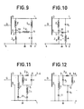
- Figures 9 to 12 show the electrical diagrams of these four cases of output impedance matching.
- the source is grounded and it is possible to decouple the parallel choke l by a capacitance 11 of high value to ground, which makes polarization very easy over a very wide band.
- the choke l which corresponds to the wiring wire of the transistor, can even be deleted and the polarization is effected by means of the two chokes L 1 and L 2 .
- FIG. 11 An embodiment of FIG. 11 in microelectronic technique or in monolithic is shown in FIG. 13.
- the capacity here is produced in interdigitated metallizations while the two decoupling capacities 11 are produced in a structure called overlay, metal-insulator-metal.
- FIG. 14 A second example of application of the impedance adapter according to the invention is given in FIG. 14: since there is an iterative impedance, it is possible to generate a periodic structure, adapted in impedance at input and at output on the same impedance Z, thanks to the adapter according to the invention, and thus to produce a traveling wave amplifier.
- This amplifier thus consists of a plurality of cells connected in cascade, each cell being constituted by a quadrupole according to the invention, whose output impedance Z constitutes the input impedance Z of the next quadrupole in the cascade.
- the input of this traveling wave amplifier is on terminal 12 and the output on terminal 13.
- the values L l , L 2 and ⁇ of the impedances of the adapter according to the invention are calculated to obtain a flat gain as a function of frequency.
- the power of each stage of the traveling wave amplifier is adjusted by varying the value of the self l of each transistor, as a function of the value of the capacitance y, which modifies the slope of the curve and consequently the power absorbed for a frequency f.
- the resonance frequencies f 0 are maximum on the side of the input terminal 12, and minimum on the side of the output terminal 13.
- Such a traveling wave amplifier is preferably produced according to the quadrupole of FIG. 2, because it allows polarization of the transistors easier than with the quadrupole of FIG. 4.
- the impedance adapter according to the invention is specified by the following claims.
Landscapes
- Engineering & Computer Science (AREA)
- Power Engineering (AREA)
- Amplifiers (AREA)
- Microwave Amplifiers (AREA)
- Filters And Equalizers (AREA)
Applications Claiming Priority (2)
| Application Number | Priority Date | Filing Date | Title |
|---|---|---|---|
| FR8311613A FR2549314B1 (fr) | 1983-07-12 | 1983-07-12 | Quadrupole d'adaptation, independante de la frequence de fonctionnement, d'une reactance, et amplificateur a ondes progressives utilisant un tel quadrupole |
| FR8311613 | 1983-07-13 |
Publications (2)
| Publication Number | Publication Date |
|---|---|
| EP0133080A1 true EP0133080A1 (de) | 1985-02-13 |
| EP0133080B1 EP0133080B1 (de) | 1988-03-09 |
Family
ID=9290763
Family Applications (1)
| Application Number | Title | Priority Date | Filing Date |
|---|---|---|---|
| EP84401410A Expired EP0133080B1 (de) | 1983-07-12 | 1984-07-03 | Frequenzunabhängiger Impedanzanpassungsvierpol und Wanderwellenverstärker der diesen verwendet |
Country Status (6)
| Country | Link |
|---|---|
| US (1) | US4635005A (de) |
| EP (1) | EP0133080B1 (de) |
| JP (1) | JPS6038911A (de) |
| CA (1) | CA1223051A (de) |
| DE (1) | DE3469833D1 (de) |
| FR (1) | FR2549314B1 (de) |
Cited By (1)
| Publication number | Priority date | Publication date | Assignee | Title |
|---|---|---|---|---|
| EP0600548A1 (de) * | 1992-12-03 | 1994-06-08 | Philips Electronics Uk Limited | In Kaskade verwendbare kompakte Mikrowellenverstärkerschaltung |
Families Citing this family (10)
| Publication number | Priority date | Publication date | Assignee | Title |
|---|---|---|---|---|
| FR2618610B1 (fr) * | 1987-07-20 | 1989-12-22 | Dassault Electronique | Dispositif de retard hyperfrequence |
| JPH04225601A (ja) * | 1990-12-27 | 1992-08-14 | Sharp Corp | 帯域除去フィルタ回路 |
| GB2258778B (en) * | 1991-08-15 | 1995-07-12 | Amulet Electronics Ltd | Impedance matching |
| US7006553B1 (en) * | 2000-10-10 | 2006-02-28 | Freescale Semiconductor, Inc. | Analog signal separator for UWB versus narrowband signals |
| DE10207070A1 (de) * | 2002-02-20 | 2003-08-28 | Varta Microbattery Gmbh | Verfahren zur Herstellung von galvanischen Elementen |
| DE602006010377D1 (de) * | 2006-08-28 | 2009-12-24 | Laird Technologies Ab | Ein raucharmer Eingangsverstärker für eine elektrische kleine Antenne |
| CN103259501B (zh) * | 2013-05-31 | 2016-06-29 | 电子科技大学 | 一种通信系统用带阻滤波器 |
| JP5695712B2 (ja) * | 2013-08-29 | 2015-04-08 | 住友電気工業株式会社 | 変圧装置 |
| WO2018165337A1 (en) * | 2017-03-10 | 2018-09-13 | Mission Microwave Components, Llc | Passive non-ferromagnetic circulator |
| CN111181500A (zh) * | 2020-02-13 | 2020-05-19 | 深圳飞骧科技有限公司 | 功率分合电路、功率放大电路、芯片及电子设备 |
Citations (1)
| Publication number | Priority date | Publication date | Assignee | Title |
|---|---|---|---|---|
| US3879689A (en) * | 1974-06-21 | 1975-04-22 | Bell Telephone Labor Inc | Matched phase shifter |
Family Cites Families (6)
| Publication number | Priority date | Publication date | Assignee | Title |
|---|---|---|---|---|
| NL39540C (de) * | 1933-01-30 | |||
| US2029014A (en) * | 1934-01-31 | 1936-01-28 | Bell Telephone Labor Inc | Wave transmission network |
| NL51737C (de) * | 1936-11-19 | |||
| FR1064891A (fr) * | 1952-10-18 | 1954-05-18 | Csf | Perfectionnements aux réseaux transformateurs d'impédances |
| BE527031A (de) * | 1953-03-16 | |||
| US3302133A (en) * | 1961-01-03 | 1967-01-31 | Telefunken Patent | Circuit |
-
1983
- 1983-07-12 FR FR8311613A patent/FR2549314B1/fr not_active Expired
-
1984
- 1984-07-03 EP EP84401410A patent/EP0133080B1/de not_active Expired
- 1984-07-03 DE DE8484401410T patent/DE3469833D1/de not_active Expired
- 1984-07-09 US US06/628,774 patent/US4635005A/en not_active Expired - Fee Related
- 1984-07-11 CA CA000458660A patent/CA1223051A/en not_active Expired
- 1984-07-12 JP JP59145204A patent/JPS6038911A/ja active Pending
Patent Citations (1)
| Publication number | Priority date | Publication date | Assignee | Title |
|---|---|---|---|---|
| US3879689A (en) * | 1974-06-21 | 1975-04-22 | Bell Telephone Labor Inc | Matched phase shifter |
Non-Patent Citations (1)
| Title |
|---|
| WIRELESS WORLD, vol. 85, no. 1524, août 1979, pages 63-66,86, Londres, GB; G. KALANIT: "Passive notch filters - 1" * |
Cited By (2)
| Publication number | Priority date | Publication date | Assignee | Title |
|---|---|---|---|---|
| EP0600548A1 (de) * | 1992-12-03 | 1994-06-08 | Philips Electronics Uk Limited | In Kaskade verwendbare kompakte Mikrowellenverstärkerschaltung |
| US5412347A (en) * | 1992-12-03 | 1995-05-02 | U.S. Philips Corporation | Compact cascadable microwave amplifier circuits |
Also Published As
| Publication number | Publication date |
|---|---|
| CA1223051A (en) | 1987-06-16 |
| US4635005A (en) | 1987-01-06 |
| FR2549314A1 (fr) | 1985-01-18 |
| JPS6038911A (ja) | 1985-02-28 |
| DE3469833D1 (en) | 1988-04-14 |
| EP0133080B1 (de) | 1988-03-09 |
| FR2549314B1 (fr) | 1985-11-08 |
Similar Documents
| Publication | Publication Date | Title |
|---|---|---|
| EP1097509B1 (de) | Vektormodulator | |
| EP0078187B1 (de) | Hochfrequenz-subharmonische-Mischanordnung und deren Verwendung in einem H.F.-Frequenzumsetzer | |
| FR2652197A1 (fr) | Transformateurs du type symetrique-dissymetrique perfectionnes. | |
| FR2696295A1 (fr) | Dispositif pour corriger les distorsions non-linéaires d'un amplificateur électronique. | |
| EP0133080B1 (de) | Frequenzunabhängiger Impedanzanpassungsvierpol und Wanderwellenverstärker der diesen verwendet | |
| EP0795957B1 (de) | Vorrichtung mit einer passiven um 180 Grad phasenverschiebenden Kopplungsschaltung | |
| EP0836271B1 (de) | Integrierter Oszillator und einen solchen Oszillator verwendendes Funktelefon | |
| EP0012093B1 (de) | Verteilter Mikrowellenverstärker und diesen Verstärker enthaltende Verstärkervorrichtung | |
| EP0148706A2 (de) | Variables Impedanzglied und sein Regelkreis | |
| FR2721156A1 (fr) | Circuit de linéarisation à prédistorsion. | |
| EP0124423A1 (de) | Hyperfrequenter Leistungsverstärker | |
| FR2862158A1 (fr) | Balun distribue a rapport d'impedance non unitaire | |
| EP0078188B1 (de) | Breitband-Hochfrequenzanordnung zur Erzeugung von harmonischer gerader Ordnung eines Eingangssignals und deren Verwendung in einem H.F.-System | |
| EP0401906B1 (de) | Phasenschieber | |
| EP0318379A1 (de) | Ultrahochfrequenzverstärker mit sehr breitem Durchlassbereich | |
| EP0237099A1 (de) | Breitbandkettenverstärkerschaltung im Ultrahochfrequenzbereich | |
| EP0596568A1 (de) | Halbleitervorrichtung mit einer monolithisch integrierten Kettenverstärkerschaltung mit grosser Bandbreite und hohem Verstärkungsgrad | |
| FR3120758A1 (fr) | Circuit de polarisation en bande de base et rf, et circuit amplificateur de puissance rf le comprenant | |
| EP0387949B1 (de) | Integrierte Halbleitervorrichtung mit einer aktiven Isolatorschaltung | |
| FR2672449A1 (fr) | Dephaseur variable analogique pour signaux hyperfrequence. | |
| EP0347985B1 (de) | Allpasstyp-Schaltung für ultrahohe Frequenzen | |
| EP0032332B1 (de) | Hochfrequenzleistungsteiler und Hochfrequenzschaltungen, insbesondere Halbleiterschaltungen mit einem solchen Teiler | |
| EP0372643B1 (de) | Integrierte Halbleiterschaltung mit einer Leistungsverstärkerstufe für Ultrahochfrequenz | |
| EP1251634A1 (de) | Transkonduktanzstufe und RF Kommunikationsvorrichtung, die eine solche Stufe umfasst | |
| EP0203663A1 (de) | Hyperfrequenzleistungsoszillator, der in einem grossen Frequenzgebiet linear moduliert ist |
Legal Events
| Date | Code | Title | Description |
|---|---|---|---|
| PUAI | Public reference made under article 153(3) epc to a published international application that has entered the european phase |
Free format text: ORIGINAL CODE: 0009012 |
|
| AK | Designated contracting states |
Designated state(s): DE GB IT NL SE |
|
| 17P | Request for examination filed |
Effective date: 19850306 |
|
| 17Q | First examination report despatched |
Effective date: 19861107 |
|
| GRAA | (expected) grant |
Free format text: ORIGINAL CODE: 0009210 |
|
| AK | Designated contracting states |
Kind code of ref document: B1 Designated state(s): DE GB IT NL SE |
|
| ITF | It: translation for a ep patent filed | ||
| REF | Corresponds to: |
Ref document number: 3469833 Country of ref document: DE Date of ref document: 19880414 |
|
| GBT | Gb: translation of ep patent filed (gb section 77(6)(a)/1977) | ||
| PLBE | No opposition filed within time limit |
Free format text: ORIGINAL CODE: 0009261 |
|
| STAA | Information on the status of an ep patent application or granted ep patent |
Free format text: STATUS: NO OPPOSITION FILED WITHIN TIME LIMIT |
|
| 26N | No opposition filed | ||
| PGFP | Annual fee paid to national office [announced via postgrant information from national office to epo] |
Ref country code: GB Payment date: 19930617 Year of fee payment: 10 |
|
| PGFP | Annual fee paid to national office [announced via postgrant information from national office to epo] |
Ref country code: SE Payment date: 19930618 Year of fee payment: 10 |
|
| PGFP | Annual fee paid to national office [announced via postgrant information from national office to epo] |
Ref country code: DE Payment date: 19930622 Year of fee payment: 10 |
|
| ITTA | It: last paid annual fee | ||
| PGFP | Annual fee paid to national office [announced via postgrant information from national office to epo] |
Ref country code: NL Payment date: 19930731 Year of fee payment: 10 |
|
| PG25 | Lapsed in a contracting state [announced via postgrant information from national office to epo] |
Ref country code: GB Effective date: 19940703 |
|
| PG25 | Lapsed in a contracting state [announced via postgrant information from national office to epo] |
Ref country code: SE Effective date: 19940704 |
|
| EUG | Se: european patent has lapsed |
Ref document number: 84401410.0 Effective date: 19950210 |
|
| PG25 | Lapsed in a contracting state [announced via postgrant information from national office to epo] |
Ref country code: NL Effective date: 19950201 |
|
| GBPC | Gb: european patent ceased through non-payment of renewal fee |
Effective date: 19940703 |
|
| NLV4 | Nl: lapsed or anulled due to non-payment of the annual fee | ||
| PG25 | Lapsed in a contracting state [announced via postgrant information from national office to epo] |
Ref country code: DE Effective date: 19950401 |
|
| EUG | Se: european patent has lapsed |
Ref document number: 84401410.0 |