EP0596568A1 - Halbleitervorrichtung mit einer monolithisch integrierten Kettenverstärkerschaltung mit grosser Bandbreite und hohem Verstärkungsgrad - Google Patents
Halbleitervorrichtung mit einer monolithisch integrierten Kettenverstärkerschaltung mit grosser Bandbreite und hohem Verstärkungsgrad Download PDFInfo
- Publication number
- EP0596568A1 EP0596568A1 EP93203038A EP93203038A EP0596568A1 EP 0596568 A1 EP0596568 A1 EP 0596568A1 EP 93203038 A EP93203038 A EP 93203038A EP 93203038 A EP93203038 A EP 93203038A EP 0596568 A1 EP0596568 A1 EP 0596568A1
- Authority
- EP
- European Patent Office
- Prior art keywords
- ground
- transistor
- pad
- source
- circuit
- Prior art date
- Legal status (The legal status is an assumption and is not a legal conclusion. Google has not performed a legal analysis and makes no representation as to the accuracy of the status listed.)
- Granted
Links
Images




Classifications
-
- H—ELECTRICITY
- H03—ELECTRONIC CIRCUITRY
- H03F—AMPLIFIERS
- H03F3/00—Amplifiers with only discharge tubes or only semiconductor devices as amplifying elements
- H03F3/60—Amplifiers in which coupling networks have distributed constants, e.g. with waveguide resonators
- H03F3/605—Distributed amplifiers
- H03F3/607—Distributed amplifiers using FET's
Definitions
- the invention relates to a semiconductor device comprising a circuit of the monolithically distributed type integrated on a substrate, operating in the high and / or microwave domain, this distributed circuit comprising a plurality of coupled stages each having at least one transistor with electrodes. , of which at least one of these electrodes, called the first electrode, is individually connected to ground alternately.
- the invention finds its application in the production of monolithically integrated microwave circuits (in English MMICS for Monolithic Microwave Integrated Circuits) for use in the field of telecommunications.
- a distributed amplifier is already known from US Pat. No. 4,853,649.
- This document describes an amplifier comprising a plurality of stages with coupled field effect transistors, the gates of which are connected to a grid line and the drains connected to a line of drain, these grid and drain lines being formed of inductances.
- the sources of the transistors are provided with a self-polarization circuit to adjust the DC source potential to a given value.
- This source self-polarization circuit which is applied individually to each transistor of the distributed amplifier, comprises a capacitor and a resistor arranged in parallel between each source and the ground.
- the capacity is used to put the source at the microwave. It must therefore have a value sufficient to produce a microwave short-circuit, for example 3 to 4 times the value of the gate-source capacitance of the transistor.
- the resistance is used to adjust the value of the source DC potential with respect to the mass. It must therefore have a value large enough for a suitable, non-negligible potential to be established at its limits.
- This resistance-capacitance arrangement produces a harmful effect which consists in the creation, or the amplification, of oscillations which already have only too much tendency to occur in a distributed amplifier with strong gain.
- this arrangement is applied to transistors of the so-called interdigital type, having a drain finger, two gate fingers arranged on either side of the drain finger, and in addition two source fingers arranged on both sides. else of the whole.
- the transistors are arranged in line on a substrate, with the electrodes parallel from one transistor to the other, the source fingers of a transistor thus being opposite a finger of source of the preceding transistor and a source finger of the following transistor, except for the first and the last transistors.
- each transistor is a metallization to form a ground pad.
- This metallization is connected to a ground plane, produced on the opposite face of the substrate, by means of a metallized hole.
- each source finger is connected by an air bridge to a planar capacitance produced on the surface of the ground stud, which therefore provides two capacitors produced in opposite between the transistors and in line with them.
- each transistor only one of the source fingers is extended by a conductive line to connect this source finger to a resistor arranged in a part of the surface of the substrate between the conductive line and the ground pad, but not in line with transistors.
- this arrangement was chosen to avoid modifying the dimensions of the microwave lines forming inductors which interconnect the drains of the transistors to form the drain line, as well as those of the microwave lines having a similar function to form the grid line.
- the capacities of the self-polarization circuits to be produced between source fingers and ground pads have, due to their function, fairly substantial dimensions; but by their planar structure they can be produced on the surface of the ground stud, and, by means of the formation of an insulation groove practiced between two facing capacities, they can be integrated without causing too great an increase in the distance between transistors.
- the two source fingers of the same transistor are not connected to each other, and only one of these fingers is provided with the RC self-polarization circuit. So the transistors in Figure 15 of the cited document each work as a half of a transistor.
- the resistances of the self-polarization circuits are arranged exactly between the sources of the transistors and the ground, because the inductances of the metallized holes connecting the ground pads to the ground plane are negligible compared to the impedances constituting these self-polarization circuits and are therefore not taken into account in their operation.
- the technology chosen to produce the distributed amplifier known from the cited document is of the microstrip type (in English MICROSTRIP).
- a first face called the front face of the substrate, which is here in GaAs, carries the active elements, conductive tapes to form the transmission lines, and metallized pads to form the ground pads.
- the second face of the substrate called the rear face, carries a metallized plane to form the mass. So that the impedance of the lines is a function of the width and the length of the conductive tapes of the first face, and of the thickness of the substrate.
- metallized holes in English VIA HOLES, located in the central parts of the ground studs are formed through the substrate, to bring the potential of the ground plane from the rear face up to these ground studs on the front face. of the substrate.
- the stray gate-drain capacitance (Cg d ) becomes a very critical parameter, and oscillations appear at frequencies higher than that of the passband of the amplifier.
- An object of the invention is to provide means for producing a device having a distributed integrated circuit, by guarding against the appearance of oscillations on the side of the high frequencies of the operating frequency band.
- said first electrode is connected to ground by two branches, a said first branch connected directly to a first stud of ground, and a second branch connected through a resistor to a second ground stud.
- An object of the invention is to provide a device having an easily integrated distributed circuit.
- this object is achieved by means of this device further characterized in that, in the distributed circuit, the stages are mounted opposite one another in such a way that, for each stage considered, the first ground stud is common with the second ground stud of the preceding stage or the following stage, and the second ground stud is common with the first ground stud of the following stage or the preceding stage respectively, so that, by this arrangement, as an alternative, in each stage considered, said first electrode of the transistor is connected on the one hand to ground by the inductance of the first ground pad, and on the other hand to said first electrodes of the preceding and following stages by the resistors of their respective second branches.
- Another object of the invention is to provide a device having an amplifier circuit whose performance is improved compared to that of the circuit known from the prior art.
- the distributed circuit is a broadband amplifier with high gain, this amplifier circuit comprising a plurality of coupled stages each having at least one field effect transistor whose source constitutes said first electrode and the gate and the drain of which are connected respectively to a so-called gate line and to a so-called drain line, formed of inductances.
- Another object of the invention is to propose a device having an amplifier circuit which is easily integrated into a very efficient technology.
- each transistor is of the interdigitated type according to which the source consists of at least two source electrode pads, called external pads, topologically arranged on either side of the other interdigitated electrode pads of this transistor, in that for each transistor, all of the source electrode pads are connected directly to each other by means of a conductor, and in that the one of the two external source electrode pads said first pad forms said first branch directly connected to the first ground pad and the other of these two external source electrode pads said second pad forms said second branch connected to the second pad mass through said resistor.
- this device is characterized in that, the transistors for forming the distributed amplifier are topologically arranged in line on the surface of the substrate, with their pads of interdigitated electrodes arranged perpendicular to this line, each transistor having said second source electrode pad facing said first source electrode pad of the next transistor of the amplifier circuit, in that the ground pads shared by these two transistors are topologically arranged between these transistors and aligned with them, so adjacent to said second and to said first facing source electrode pads, and in that for each transistor said low value resistance is topologically produced by overlapping between said second source electrode pad and the ground pad which is adjacent thereto .
- Another object of the invention is to provide means for producing a device having a distributed amplifier circuit whose bandwidth is increased towards the high frequencies, without however showing a risk of oscillations on the side of the high frequencies.
- each stage of the distributed amplifier is of the cascode type in which one associates with each transistor said low transistor of the distributed amplifier mounted as a common source to ground , a so-called high transistor, which is mounted in a grid common to ground at high and / or microwave, grid which constitutes said first electrode of this cascode stage and which is isolated from ground continuously by capacitors.
- the invention applies to many distributed circuits operating at high and / or microwave frequencies and in particular to distributed amplifiers and to distributed mixers.
- the latter have a structure comparable to that of distributed amplifiers of the cascode type.
- the description below relates, by way of example, to a distributed amplifier circuit integrated in a semiconductor device.
- a distributed amplifier shown by way of nonlimiting example, comprises a plurality of field effect transistors Ti, T 2 ... T N ... mounted as a common source, a first line L G formed of sections of microwave impedance lines LG ,, LG 2 ... LG N + L respectively, and a second line L o formed of sections of microwave lines of impedance LD 1 , LD 2 ... respectively.
- the gates of the transistors T 1 , T 2 ... are connected periodically to the line L G called the gate line, between the sections of microwave lines LG,, LG 2 ... respectively.
- the drains of the transistors T 1 , T 2 ... are connected periodically to the line L o called the drain line, between the sections of microwave lines LD 1 , LD 2 ... respectively.
- a microwave input signal E is applied to this amplifier on the end of the grid line L G , and the amplified microwave output O is taken from the end of the drain line.
- the inherent impedances LG ,, LG 2 of the grid line L G form, with the intrinsic gate-source capacities of the field effect transistors Ti, T 2, etc., a distributed microwave line called the artificial transmission line.
- drain line L D between the own impedances LD 1 , LD 2 and the drain-source capacities of the field effect transistors Ti, T 2 ...
- the operating principle of the distributed amplifier is based on the propagation of the signals along the artificial transmission lines thus formed.
- the microwave signal E When the microwave signal E is applied to the gate line, it propagates by exciting each transistor which then provides an output power capable of propagating on the drain line. If the phase speed of the two artificial transmission lines is identical, the power is added in phase during propagation along the drain line. It is then possible to obtain an amplification in a frequency band, which is limited inter alia by the cut-off frequency of the transmission lines.
- the sections LG 1 , LG 2 , .. LD 1 , LD 2 ... can represent small sections of transmission lines for frequencies such as 20 GHz.
- the length of these sections is calculated so as to ensure the phase shift necessary for the proper functioning of the amplifier.
- the amplifier further comprises at least one bias circuit.
- a polarization circuit P is provided at the end of the line L o opposite the output O.
- This polarization circuit P consists for example of sections of microwave transmission lines L 21 , L 22 , L 23 ... and of capacities C 21 , C 22 , C 23 mounted between the mass and the connection nodes between each of these sections L 21 , L 22 , L 23 ...
- the grid and drain lines L G and L o are further closed on a load respectively Z G and Z D.
- the load applied to the grid line L G can be formed by a resistor R 30 and a capacitor C 30 connected in series and placed between the output of the line L G and the ground.
- the operating frequency of such a distributed amplifier is theoretically limited on the one hand by the cut-off frequency of the field effect transistors, and on the other hand by the cut-off frequency of the artificial lines as said above.
- the actual cutoff frequency of the circuit is much lower than these theoretical frequencies, because this cutoff frequency is limited by multiple reflections and resonance phenomena which result therefrom. These phenomena are due to the variation of the characteristic impedances of the lines when the operating frequency varies, and the mere improvement of the polarization is not enough to eliminate these phenomena. These reflective phenomena appear in particular on the grid line at the level of the plane AA 'between the last section of line LN + and the load Z G , the wave on the grid line propagating from the input E in the direction of this charge Z G.
- Each cascode stage comprises, mounted between the drain of transistor T 1 , T 2 , T N of a stage of the conventional distributed amplifier, and the drain line L D , an additional transistor T ' 1 , T' 2 .. T ' N , the grid of which is connected to ground through a capacity, respectively Ci, C 2 , C N.
- the cascode assembly therefore consists in associating, in each stage of the distributed amplifier, a high transistor T ' 1 , T' 2 ... T ' N mounted in a common gate, which is grounded at microwave frequencies through the capacitance d 'continuous insulation Ci ... C N , to a low transistor T 1 , T 2 , ... T N mounted as a common source.
- the advantage is obtained that the coupling between the gate and drain lines is reduced, and that, in this way, the bandwidth of the distributed amplifier circuit is notably increased on the side of the high frequencies without loss of gain.
- the different active elements are linked to each other and to the grid line and drain line by sections of microwave lines.
- drains of the high transistors T ' 1 , T' 2 , ... T ' N are connected to the drain line by lines, respectively P 1 , P 2 ... P N , the drain line then being consisting of line sections PD 1 , PD 2 , ... PD N +1.
- the high and low transistors, T'i and T 1 , T ' 2 and T 2 , T' N and T N are connected by lines PA 1 , PA2, PA N respectively .
- the gates of the high transistors are connected to each other by line sections PG 1 , PG 2 , PG N.
- the grid line consists of line sections LG 1 , LG 2 ... LG N + 1 .
- the section of line placed on the drain of the transistor T 1 in the position LG 1 is not part of the load Z D but indeed of the drain line L D.
- the line section placed on the gate of the transistor T N in the position of LG N + 1 is not part of the load Z G , but indeed of the gate line L G. This is due to the very principle of a distributed amplifier.
- the amplifier distributed according to FIG. 2b is formed of a number of 5 field effect transistors.
- the transmission line sections are of the microstrip type.
- the drain line is biased through a circuit P connected to a direct voltage V D , applied at the end opposite to the output O
- the gate line is biased through a circuit P 'connected to a DC voltage V G1 applied at the end opposite the input E
- the gate line of the high transistors mounted in cascode is biased at its output end through a circuit P "connected to a continuous supply V G2 .
- the bias circuits P, P ', P" are preferably constituted by inductors.
- the values of the DC bias voltages V D , V G1 , V G2 are given in table I.
- resistors R 2 .... R N + 1 into the grid line of the cascode transistors is an important factor of stability.
- the present invention offers a solution to this problem insofar as the amplifier is produced in a technology including intergity transistors of which one of the electrodes, called the first electrode, in this case the source electrode, is connected to ground by mass pads of large area.
- the distributed amplifier circuits are preferably produced by means of a technology of interdigitated transistors, these transistors can be both MESFETs and HEMTs with several gate fingers ( at least two), one or more drain fingers and several source fingers (at least two) of which at least one source finger is disposed on either side of the other fingers.
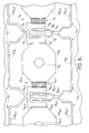
- a transistor of the Nth stage of the amplifier comprises at least one drain finger D N , disposed between two gate fingers G N , G ' N and G “ N respectively ; it also includes two contacts (or pads) of source electrode S N , respectively S ' N and S " N , called first and second pads of source electrode, arranged on the other side of the gate fingers G' N , G" N , with respect to the drain finger D N.
- the drain finger D N is connected to the line sections LD N and LD N + L of the drain line L o by portions of line, and the two gate fingers G ' N , G " N are first joined , then connected to the line sections LG N and LG N + 1 of the grid line L G also by line portions.
- the source contacts said peripheral (or external) S ' N and S " N are respectively adjacent to the ground pads VH N and VH N + 1 respectively.
- FIG. 3c shows two successive stages comprising the transistors T N - 1 and T N , of a distributed amplifier as shown diagrammatically in FIG. 1, and not, for reasons of simplicity of drawing, corresponding to the cascode mount amplifier of Figures 2a or 2b. Those skilled in the art will easily make the necessary transposition to apply the invention to all kinds of amplifiers.
- the substrates are chosen from semiconductor materials, favorably from the III-V group such as for example gallium arsenide (GaAs), but many other semiconductor or ceramic materials are possible.
- the technology is chosen of the microstrip type, (in English MICROSTRIP) in which the ribbon-shaped conductors constituting lines, and the active elements, are on one of the faces of the substrate, the other face of this substrate carrying a ground plan.
- the integration density of the elements can be high.
- all the electrodes of the corresponding transistors of all the stages are arranged in parallel, and moreover these transistors are in line, so that the peripheral source electrodes are each opposite a electrode. source from a previous or next floor, except for the first and last floors.
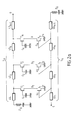
- FIG. 3a schematically represents the two circuit stages corresponding to the topology of FIG. 3c
- FIG. 3b shows the diagram equivalent to the circuit part of FIG. 3a.
- the metallized holes Hi, H 2 ... H N associated with the studs VH ,, VH 2 ... VH N , arranged in accordance with the topology of FIG. 3c, have, as shown in FIG. 3b, a low inductance value, which does not significantly degrade, the performance of the transistor of the corresponding stage, in its high and / or microwave operating range.
- microstrip technology which includes ground studs with metallized holes as illustrated in Figures 3, is not limiting.
- the invention can be implemented in any technology where the mass pads of large area Hi ... H N + 1 are connected to ground lines of low characteristic impedance as in coplanar technology for example.
- each transistor source therefore sees an impedance of:
- FIG. 4 which shows the amplitude in dB of the coefficient S21 of a distributed amplifier with cascode stage, it appears on curve A in broken line of the oscillations at high frequencies, when no measurement is taken for the remove.
- the distributed amplifier must see both its increased bandwidth, a high gain maintained, and the possibility of the appearance of oscillations at frequencies higher than those of the bandwidth, completely eliminated.
- the solution found for preventing oscillations, without degrading the gain resides in a means which consists in placing a resistance r of low value between only one of the source fingers and its corresponding metallized ground pad.
- a resistor of small value r N will be placed in the stage of the transistor T N , between the source electrode pad S " N , called the second source electrode pad, and the ground stud VH N.
- the two (or more) fingers (or pads) of source S ' N -S " N will be connected to each other by a conductor S N produced at a level other than the other parts of the transistor (in FIG. 3c the drain finger D N ) that this conductor must cross, and the same in all stages of the amplifier.
- the source of a transistor sees on the one hand in a branch a direct connection with a ground pad provided with a hole metallized by one of the electrode fingers (or pads) source (for example said first pad S ' N and H N - VH N ) and on the other hand, in parallel, in another branch, a connection of the source electrode with a second ground pad provided with a metallized hole (for example said second pad S " N and H N + 1 - VH N + 1 ), through a resistance r N of low value.
- each transistor T N is connected on the one hand to ground by a branch containing only a low inductance of 20 pH, that is to say 2.5 ⁇ at 20 GHz, and on the other hand to the sources of the preceding and following transistors by branches containing said low resistance r N.
- the source S N of the transistor T N sees an impedance given below by Z N and which is relative to a low inductance L N corresponding to H N - VH N arranged between the source node S N and the ground, with in parallel, a low inductance LN + corresponding to H N + 1 - VH N + 1 in series with said low resistance r N arranged between the source node S N and the mass.
- Z N the impedance given below by Z N and which is relative to a low inductance L N corresponding to H N - VH N arranged between the source node S N and the ground, with in parallel, a low inductance LN + corresponding to H N + 1 - VH N + 1 in series with said low resistance r N arranged between the source node S N and the mass.
- ground studs have a structure different from that which is presented in FIGS. 3, for example ground studs not provided with metallized holes, but connected to ground lines of low characteristic impedance as in coplanar technology for example.
Landscapes
- Engineering & Computer Science (AREA)
- Power Engineering (AREA)
- Microwave Amplifiers (AREA)
Applications Claiming Priority (2)
| Application Number | Priority Date | Filing Date | Title |
|---|---|---|---|
| FR9213242A FR2697698A1 (fr) | 1992-11-04 | 1992-11-04 | Dispositif semiconducteur comprenant un circuit amplificateur distribué monolithiquement intégré, à large bande et fort gain. |
| FR9213242 | 1992-11-04 |
Publications (2)
| Publication Number | Publication Date |
|---|---|
| EP0596568A1 true EP0596568A1 (de) | 1994-05-11 |
| EP0596568B1 EP0596568B1 (de) | 1998-04-29 |
Family
ID=9435196
Family Applications (1)
| Application Number | Title | Priority Date | Filing Date |
|---|---|---|---|
| EP93203038A Expired - Lifetime EP0596568B1 (de) | 1992-11-04 | 1993-10-29 | Halbleitervorrichtung mit einer monolithisch integrierten Kettenverstärkerschaltung mit grosser Bandbreite und hohem Verstärkungsgrad |
Country Status (5)
| Country | Link |
|---|---|
| US (1) | US5386130A (de) |
| EP (1) | EP0596568B1 (de) |
| JP (1) | JPH06224663A (de) |
| DE (1) | DE69318253T2 (de) |
| FR (1) | FR2697698A1 (de) |
Families Citing this family (10)
| Publication number | Priority date | Publication date | Assignee | Title |
|---|---|---|---|---|
| US6026286A (en) * | 1995-08-24 | 2000-02-15 | Nortel Networks Corporation | RF amplifier, RF mixer and RF receiver |
| JPH09121127A (ja) * | 1995-10-26 | 1997-05-06 | Murata Mfg Co Ltd | 高周波増幅集積回路装置 |
| US6049250A (en) * | 1998-04-03 | 2000-04-11 | Trw Inc. | Dittributed feed back distributed amplifier |
| US6081006A (en) * | 1998-08-13 | 2000-06-27 | Cisco Systems, Inc. | Reduced size field effect transistor |
| KR100378676B1 (ko) * | 2000-09-07 | 2003-03-31 | 광주과학기술원 | 파이형 출력 전송선 구조를 갖는 진행파 증폭기 |
| FR2826802B1 (fr) * | 2001-06-28 | 2003-09-26 | Cit Alcatel | Dispositif de polarisation a large bande de frequences d'un circuit electronique et amplificateur l'incorporant |
| JP2003174338A (ja) * | 2001-12-05 | 2003-06-20 | Murata Mfg Co Ltd | 分布増幅器および分布差動増幅器 |
| JP6430806B2 (ja) * | 2014-12-18 | 2018-11-28 | 日本電信電話株式会社 | 分布ミキサ |
| BR112018015791A2 (pt) | 2016-02-04 | 2018-12-26 | Fraunhofer Ges Forschung | amplificador de potência em matriz |
| JP6837602B2 (ja) | 2018-05-09 | 2021-03-03 | 三菱電機株式会社 | 分布型増幅器 |
Citations (5)
| Publication number | Priority date | Publication date | Assignee | Title |
|---|---|---|---|---|
| GB2146195A (en) * | 1981-03-26 | 1985-04-11 | Raytheon Co | Radio frequency network having plurality electrically interconnected field effect transistor cells |
| DE3726743A1 (de) * | 1986-09-01 | 1988-03-03 | Mitsubishi Electric Corp | Fet-kettenverstaerker |
| US4853649A (en) * | 1987-02-12 | 1989-08-01 | Mitsubishi Denki Kabushiki | Distributed fet amplifier and bias voltage supply circuit therefor |
| US4864250A (en) * | 1987-01-29 | 1989-09-05 | Harris Corporation | Distributed amplifier having improved D.C. biasing and voltage standing wave ratio performance |
| EP0472357A2 (de) * | 1990-08-22 | 1992-02-26 | Mitsubishi Denki Kabushiki Kaisha | Integrierter Halbleiterschaltkreis |
Family Cites Families (6)
| Publication number | Priority date | Publication date | Assignee | Title |
|---|---|---|---|---|
| IT1038800B (it) * | 1975-06-10 | 1979-11-30 | Ates Componenti Elettron | Tranistore planare di potenza |
| US4456888A (en) * | 1981-03-26 | 1984-06-26 | Raytheon Company | Radio frequency network having plural electrically interconnected field effect transistor cells |
| JPS594175A (ja) * | 1982-06-30 | 1984-01-10 | Fujitsu Ltd | 電界効果半導体装置 |
| GB2211988B (en) * | 1987-11-03 | 1992-04-01 | Stc Plc | Current matching of bipolar transistors |
| US4939485A (en) * | 1988-12-09 | 1990-07-03 | Varian Associates, Inc. | Microwave field effect switch |
| JP3063167B2 (ja) * | 1989-12-29 | 2000-07-12 | 日本電気株式会社 | 電流検出端子付mos fetおよびその製造方法 |
-
1992
- 1992-11-04 FR FR9213242A patent/FR2697698A1/fr not_active Withdrawn
-
1993
- 1993-10-29 EP EP93203038A patent/EP0596568B1/de not_active Expired - Lifetime
- 1993-10-29 DE DE69318253T patent/DE69318253T2/de not_active Expired - Lifetime
- 1993-11-02 US US08/146,765 patent/US5386130A/en not_active Expired - Lifetime
- 1993-11-04 JP JP5275550A patent/JPH06224663A/ja active Pending
Patent Citations (5)
| Publication number | Priority date | Publication date | Assignee | Title |
|---|---|---|---|---|
| GB2146195A (en) * | 1981-03-26 | 1985-04-11 | Raytheon Co | Radio frequency network having plurality electrically interconnected field effect transistor cells |
| DE3726743A1 (de) * | 1986-09-01 | 1988-03-03 | Mitsubishi Electric Corp | Fet-kettenverstaerker |
| US4864250A (en) * | 1987-01-29 | 1989-09-05 | Harris Corporation | Distributed amplifier having improved D.C. biasing and voltage standing wave ratio performance |
| US4853649A (en) * | 1987-02-12 | 1989-08-01 | Mitsubishi Denki Kabushiki | Distributed fet amplifier and bias voltage supply circuit therefor |
| EP0472357A2 (de) * | 1990-08-22 | 1992-02-26 | Mitsubishi Denki Kabushiki Kaisha | Integrierter Halbleiterschaltkreis |
Non-Patent Citations (1)
| Title |
|---|
| M.M. ODA: "A STABLE GAAS 6-20 GHZ HIGH GAIN AND POWER TWA", 1991 IEEE MTT-S INTERNATIONAL MICROWAVE SYMPOSIUM DIGEST, vol. 2, 10 June 1991 (1991-06-10), BOSTON US, pages 437 - 440, XP000260461 * |
Also Published As
| Publication number | Publication date |
|---|---|
| FR2697698A1 (fr) | 1994-05-06 |
| US5386130A (en) | 1995-01-31 |
| EP0596568B1 (de) | 1998-04-29 |
| DE69318253D1 (de) | 1998-06-04 |
| DE69318253T2 (de) | 1998-11-19 |
| JPH06224663A (ja) | 1994-08-12 |
Similar Documents
| Publication | Publication Date | Title |
|---|---|---|
| EP0459571B1 (de) | Langsam-Wellen-Mikrostreifenübertragungsleitung und Anordnung mit einer solchen Leitung | |
| EP0872954B1 (de) | Akustische Oberflächenwellenanordnung mit Nahfeldkopplung und differentiellen Ein- und Ausgängen | |
| EP0596568B1 (de) | Halbleitervorrichtung mit einer monolithisch integrierten Kettenverstärkerschaltung mit grosser Bandbreite und hohem Verstärkungsgrad | |
| EP0012093B1 (de) | Verteilter Mikrowellenverstärker und diesen Verstärker enthaltende Verstärkervorrichtung | |
| EP0800211A1 (de) | Integriertes Schaltungsgehäuse | |
| EP0545809A1 (de) | Vorrichtung zum Montieren von breitbandigen monolitisch integrierten Mikrowellenschaltungen | |
| EP0047690A1 (de) | Mehrere Transistoren enthaltender, monolithischer Verstärker mit Leistungsteilung und Leistungszusammenführung | |
| EP0133080B1 (de) | Frequenzunabhängiger Impedanzanpassungsvierpol und Wanderwellenverstärker der diesen verwendet | |
| EP0078188B1 (de) | Breitband-Hochfrequenzanordnung zur Erzeugung von harmonischer gerader Ordnung eines Eingangssignals und deren Verwendung in einem H.F.-System | |
| FR2964499A1 (fr) | Ligne de transmission haute frequence accordable | |
| EP0237099A1 (de) | Breitbandkettenverstärkerschaltung im Ultrahochfrequenzbereich | |
| EP0199332B1 (de) | Empfänger für optische Breitbandsignale | |
| EP0387949B1 (de) | Integrierte Halbleitervorrichtung mit einer aktiven Isolatorschaltung | |
| EP0321046A1 (de) | Hyperfrequenzschaltung mit mindestens einem belasteten Feldeffekt-Transistor | |
| EP0347985B1 (de) | Allpasstyp-Schaltung für ultrahohe Frequenzen | |
| EP0801467B1 (de) | Kettenverstärkender Adapter niedriger Impedanz für einen optoelektronischen Mikrowellensender mit sehr grosser Bandbreite | |
| EP1017171B1 (de) | Phasensteuervorrichtung mit einer Vielzahl von Kettenverstärkerstrukturen mit schaltbaren aktiven Elementen zur Erstellung einer Übertragungsleitung mit programmierbarer Länge | |
| WO1993013595A1 (fr) | Filtre a ondes de surface | |
| EP0986170A1 (de) | Schnittstelle zwischen einem breitbandigen optoelektronischen Sensor für Hyperfrequenzen und einer Last | |
| FR2550889A1 (fr) | Dispositif amplificateur a effet de champ, fonctionnant dans les hyperfrequences, par transfert d'electrons | |
| EP1271767A1 (de) | Vorrichtung zur Einstellung der Vorspannung für eine breitbandige elektronische Vorrichtung und zugehöriger Verstärker | |
| FR2640444A1 (de) | ||
| FR2597680A1 (fr) | Dispositif semiconducteur incluant un circuit amplificateur-melangeur distribue. | |
| FR2507017A1 (fr) | Microassemblage utilisable en hyperfrequences | |
| EP0656685B1 (de) | Verstärkervorrichtung mit Rückkopplung |
Legal Events
| Date | Code | Title | Description |
|---|---|---|---|
| PUAI | Public reference made under article 153(3) epc to a published international application that has entered the european phase |
Free format text: ORIGINAL CODE: 0009012 |
|
| AK | Designated contracting states |
Kind code of ref document: A1 Designated state(s): DE FR GB IT |
|
| RAP1 | Party data changed (applicant data changed or rights of an application transferred) |
Owner name: N.V. PHILIPS' GLOEILAMPENFABRIEKEN Owner name: LABORATOIRES D'ELECTRONIQUE PHILIPS |
|
| 17P | Request for examination filed |
Effective date: 19941019 |
|
| RAP1 | Party data changed (applicant data changed or rights of an application transferred) |
Owner name: PHILIPS ELECTRONICS N.V. Owner name: LABORATOIRES D'ELECTRONIQUE PHILIPS S.A.S. |
|
| GRAG | Despatch of communication of intention to grant |
Free format text: ORIGINAL CODE: EPIDOS AGRA |
|
| 17Q | First examination report despatched |
Effective date: 19970630 |
|
| GRAG | Despatch of communication of intention to grant |
Free format text: ORIGINAL CODE: EPIDOS AGRA |
|
| GRAH | Despatch of communication of intention to grant a patent |
Free format text: ORIGINAL CODE: EPIDOS IGRA |
|
| GRAH | Despatch of communication of intention to grant a patent |
Free format text: ORIGINAL CODE: EPIDOS IGRA |
|
| GRAA | (expected) grant |
Free format text: ORIGINAL CODE: 0009210 |
|
| AK | Designated contracting states |
Kind code of ref document: B1 Designated state(s): DE FR GB IT |
|
| REF | Corresponds to: |
Ref document number: 69318253 Country of ref document: DE Date of ref document: 19980604 |
|
| ITF | It: translation for a ep patent filed | ||
| GBT | Gb: translation of ep patent filed (gb section 77(6)(a)/1977) |
Effective date: 19980603 |
|
| RAP4 | Party data changed (patent owner data changed or rights of a patent transferred) |
Owner name: KONINKLIJKE PHILIPS ELECTRONICS N.V. Owner name: LABORATOIRES D'ELECTRONIQUE PHILIPS S.A.S. |
|
| PLBE | No opposition filed within time limit |
Free format text: ORIGINAL CODE: 0009261 |
|
| 26N | No opposition filed | ||
| REG | Reference to a national code |
Ref country code: FR Ref legal event code: TP |
|
| REG | Reference to a national code |
Ref country code: GB Ref legal event code: IF02 |
|
| PG25 | Lapsed in a contracting state [announced via postgrant information from national office to epo] |
Ref country code: IT Free format text: LAPSE BECAUSE OF NON-PAYMENT OF DUE FEES Effective date: 20051029 |
|
| REG | Reference to a national code |
Ref country code: GB Ref legal event code: 732E |
|
| REG | Reference to a national code |
Ref country code: GB Ref legal event code: 732E |
|
| REG | Reference to a national code |
Ref country code: FR Ref legal event code: TP |
|
| REG | Reference to a national code |
Ref country code: FR Ref legal event code: GC |
|
| REG | Reference to a national code |
Ref country code: FR Ref legal event code: RG |
|
| PGFP | Annual fee paid to national office [announced via postgrant information from national office to epo] |
Ref country code: DE Payment date: 20100930 Year of fee payment: 18 |
|
| PGFP | Annual fee paid to national office [announced via postgrant information from national office to epo] |
Ref country code: GB Payment date: 20110926 Year of fee payment: 19 |
|
| PGFP | Annual fee paid to national office [announced via postgrant information from national office to epo] |
Ref country code: FR Payment date: 20111118 Year of fee payment: 19 |
|
| GBPC | Gb: european patent ceased through non-payment of renewal fee |
Effective date: 20121029 |
|
| REG | Reference to a national code |
Ref country code: FR Ref legal event code: ST Effective date: 20130628 |
|
| PG25 | Lapsed in a contracting state [announced via postgrant information from national office to epo] |
Ref country code: GB Free format text: LAPSE BECAUSE OF NON-PAYMENT OF DUE FEES Effective date: 20121029 Ref country code: DE Free format text: LAPSE BECAUSE OF NON-PAYMENT OF DUE FEES Effective date: 20130501 |
|
| REG | Reference to a national code |
Ref country code: DE Ref legal event code: R119 Ref document number: 69318253 Country of ref document: DE Effective date: 20130501 |
|
| PG25 | Lapsed in a contracting state [announced via postgrant information from national office to epo] |
Ref country code: FR Free format text: LAPSE BECAUSE OF NON-PAYMENT OF DUE FEES Effective date: 20121031 |