EP0133771A2 - Amplificateur à champs croisés à signal d'entrée appliqué sur la cathode - Google Patents
Amplificateur à champs croisés à signal d'entrée appliqué sur la cathode Download PDFInfo
- Publication number
- EP0133771A2 EP0133771A2 EP84305032A EP84305032A EP0133771A2 EP 0133771 A2 EP0133771 A2 EP 0133771A2 EP 84305032 A EP84305032 A EP 84305032A EP 84305032 A EP84305032 A EP 84305032A EP 0133771 A2 EP0133771 A2 EP 0133771A2
- Authority
- EP
- European Patent Office
- Prior art keywords
- cathode
- slow
- wave
- anode
- circuit
- Prior art date
- Legal status (The legal status is an assumption and is not a legal conclusion. Google has not performed a legal analysis and makes no representation as to the accuracy of the status listed.)
- Withdrawn
Links
Images

Classifications
-
- H—ELECTRICITY
- H01—ELECTRIC ELEMENTS
- H01J—ELECTRIC DISCHARGE TUBES OR DISCHARGE LAMPS
- H01J25/00—Transit-time tubes, e.g. klystrons, travelling-wave tubes, magnetrons
- H01J25/34—Travelling-wave tubes; Tubes in which a travelling wave is simulated at spaced gaps
- H01J25/42—Tubes in which an electron stream interacts with a wave travelling along a delay line or equivalent sequence of impedance elements, and with a magnet system producing an H-field crossing the E-field
- H01J25/44—Tubes in which an electron stream interacts with a wave travelling along a delay line or equivalent sequence of impedance elements, and with a magnet system producing an H-field crossing the E-field the forward travelling wave being utilised
Definitions
- the invention pertains to crossed-field amplifier tubes particularly tubes in which the input signal is applied to a slow-wave interaction circuit which is part of the cathode electrode.
- a stream of electrons flows between an extended cathode surface and a generally parallel anode surface. At least a part of the anode is a wave propagating circuit with a wave velocity matched to the drift velocity of the electron stream in the crossed electric and magnetic fields.
- the electron stream is substantially confined to a thin layer near the cathode surface.
- An input wave on the anode circuit has small rf electric fields near the cathode, so the build-up of the trajectory modulation to produce electrons striking the cathode with energy to produce secondary emission multiplication is slow. Also the formation of charge spokes which induce waves in the output part of the circuit is delayed.
- Energy reflected from the output of the anode circuit can be coupled back to form a backward wave in the cathode circuit.
- This backward wave •can be partially re-reflected at the input of the cathode circuit.
- the resulting forward wave is regenerative and can lead to instabilities.
- a second problem is that waves on the anode circuit set up fields near the cathode circuit which can interfere with the build up of space charge under control of the input circuit.
- FIG. 1 illustrates a prior-art CFA which comprises an input slow-wave circuit in the cathode and an output slow-wave circuit in the anode.
- the cathode structure 10 comprises a metallic block 12 as of OFHC copper, extended in the direction of electron drift in the crossed D.C. electric and magnetic fields in the open space 14 between cathode structure 12 and a parallel opposed anode structure 16.
- Anode structure 16 is typically operated at ground potential and forms a part of the tube's vacuum envelope 18.
- Cathode structure 10 is operated at a negative potential such that electron are drawn from it toward anode structure 16.
- a magnetic field is applied perpendicular to the plane of FIG. 1 causing the electrons to drift toward the right in the well-known crossed-field interaction.
- Cathode block 12 is supported by one or more rods 20 mounted through dielectric insulating cylinders 22 forming part of vacuum envelope 18.
- Rods 20 may be replaced by hollow tubes (not shown) for carrying a fluid to cool cathode block 12.
- a portion 24 of cathode structure 10, embedded in cathode block 12, is constructed as a slow-wave circuit having a wave velocity comparable to the drift velocity of electrons in the crossed fields.
- slow-wave circuit 24 is a meander line formed by a meandering conductor 26 attached along its bottom side to cathode block 12 via ceramic supports 27.
- An input rf signal is coupled to the upstream end of slow wave circuit 24 through a coaxial transmission line 28.
- the outer conductor 30 of transmission line 28 is electrically integral with cathode block 12.
- the center conductor 32 passes inside outer conductor 30 and connects directly with the end of meandering conductor 26 to introduce the rf drive signal.
- Coaxial line 28 is vacuum-sealed by a transverse dielectric window 34 and is mounted on and insulated from vacuum envelope 18 by a high-voltage coaxial dielectric seal 36.
- the initial electron stream for the amplifier comes from a thermionic cathode 38 mounted in a recess 40 in cathode block 12. It is heated by a radiant heater 42 which is supplied with heating current via an insulating vacuum seal 44.
- This electron current passes between the slow-wave circuits 24, 52 and is interacted on by the rf wave on the cathode circuit 24 in such a way as to produce rf electron bunching and selective bombardment of the cathode 10 by the electrons bunched in that phase of the rf wave wherein they gain energy from the rf wave.
- the surface 46 of cathode structure 10 facing the electron stream may be coated with a material having high secondary emission to increase the available electron current.
- a block of lossy dielectric 50 absorbs any remaining wave energy in the circuit.
- the high- level amplification and power extraction is provided by a second slow-wave interaction circuit 52 embedded in anode block 16.
- Output circuit 52 is similar to input circuit 24. Its input end is terminated by a second lossy dielectric block 54. The downstream, output end of circuit 52 is directly connected via a coaxial-to-waveguide transducer 56 to an output waveguide 58 sealed by a dielectric vacuum window 60. The output power is carried by waveguide 58 to the external useful load (not shown). Beyond the output end of slow-wave circuit 52 the surface 62 of anode block 16 facing cathode block 12 is tapered closer to cathode 12. This causes collection of the spent electron stream over an extended area to spread out the heat dissipation.
- Anode block 16 may be cooled by fluid coolant passages or external air fins (not shown).
- the purpose of the prior-art arrangement of FIG. 1 is to provide a crossed-field amplifier with isolated input and output circuits and with high gain.
- the cathode was a smooth surface.
- the anode contained the slow-wave circuit, connected to an input transmission line at one end and the output transmission line at the other. Near the input, where the rf signal was small, the electron stream is confined to a thin ribbon near the cathode by the transverse magnetic field.
- the small rf electric field from the slow-wave circuit is a fringing field from the main electric field between adjacent anode segments. It decays somewhat exponentially with distance from the anode tips and is practically short-circuited by the conductive smooth cathode.
- the amplifier of FIG. 1 has however proven to be unsatisfactory due to regenerative instability.
- One basic cause is that matches between slow-wave circuits and external transmission lines are always imperfect. Particularly if a wide frequency range is to be covered, there is some residual wave reflection at the junction. Also, mismatches to the external signal generator and load create reflections.
- a large reflected wave in the output circuit 52 can, by electromagnetic coupling, generate a small backward wave in input circuit 24. This may be partially reflected at the input end of circuit 24 to produce a regenerated forward wave. Thus the spurious signal can build up until oscillation is produced.
- Another distorting process is interference by a large reverse directed wave on the anode circuit with the build-up of charge through the secondary emission multiplication process near the input.
- a large reverse directed wave can occur as a result of reflections of the output wave from the load.
- the reverse directed wave is non-synchronous with the forward directed electron flow at the input, its fields still exert a significant influence on the relatively short electron trajectories in the charge build-up region.
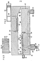
- FIG. 2 illustrates a crossed-field amplifier tube embodying the invention.
- the parts are structurally and functionally similar to those of FIG. 1, but the tube has a very important distinction.
- the portion 64 of anode block 16 opposite cathode slow-wave circuit 24 is smooth, so it does not carry waves at any velocity near that of the electron stream or the input circuit 24.
- the output circuit 52 is removed downstream of input circuit 24 and the surface 66 of cathode block 12 opposite anode circuit 52 is smooth.
- the electron stream is modulated by cathode circuit 24. After passing beyond circuit 24 the stream carries the signal as a spatially modulated travelling charge pattern.
- the beam charge induces an electromagnetic wave in anode circuit 52. This wave is amplified by interaction of circuit 52 and the beam and coupled to the useful load by output waveguide 58.
- No wave, forward or backward, on anode circuit 52 can couple energy back to cathode circuit 24 because they are spatially removed and because the electron stream moves only from input to output and cannot carry retrograde modulation.
- the amplifier is made much more stable and greatly increased gain may be obtained.
- part 68 of the surface facing anode block 16 may be formed of a material with low secondary emission yield. Electrons returning to this surface will not be fully replenished through secondary emission multiplication. As a consequence, charge will be drained from the space between electrodes and only a reduced number of electrons will enter the collector region to be collected on the high-potential anode where their bombarding energy is much higher.
- F IG. 3 is a partial section of the CFA of FIG. 2 taken on the horizontal plane 3. It illustrates the form of the meander-line slow-wave circuit formed by the meandering conductor 26. The input coupling via coaxial line 28 attached directly to the end of conductor 26 is also shown.
- the described embodiment of the invention is in a non-reentrant CFA. It is intended to be illustrative and not limiting. Many other embodiments will become obvious to those skilled in the art.
- the crossed-field amplifier may be in a circular form and/or with a recirculating electron stream. In this case a long drift space free of rf waves would follow the output circuit. It could incorporate irregular geometries to "scramble" the electron stream to remove any residual modulation.
- the meander-line circuits may be replaced by any of the other known slow-wave circuits, for example, coupled individual vanes, helix coupled bars, stub-supported meander lines, etc.
- the degree of displacement of the anode circuit beyond the end of the cathode circuit may vary, depending on the particular tube design. For moderate gain tubes, the circuits may overlap to some extent. The scope of the invention is to be limited only by the following claims and their legal equivalents.
Landscapes
- Microwave Tubes (AREA)
- Microwave Amplifiers (AREA)
- Amplifiers (AREA)
Applications Claiming Priority (2)
| Application Number | Priority Date | Filing Date | Title |
|---|---|---|---|
| US06/518,719 US4608520A (en) | 1983-07-29 | 1983-07-29 | Cathode driven crossed-field amplifier |
| US518719 | 1983-07-29 |
Publications (2)
| Publication Number | Publication Date |
|---|---|
| EP0133771A2 true EP0133771A2 (fr) | 1985-03-06 |
| EP0133771A3 EP0133771A3 (fr) | 1986-10-08 |
Family
ID=24065182
Family Applications (1)
| Application Number | Title | Priority Date | Filing Date |
|---|---|---|---|
| EP84305032A Withdrawn EP0133771A3 (fr) | 1983-07-29 | 1984-07-24 | Amplificateur à champs croisés à signal d'entrée appliqué sur la cathode |
Country Status (4)
| Country | Link |
|---|---|
| US (1) | US4608520A (fr) |
| EP (1) | EP0133771A3 (fr) |
| JP (1) | JPS6044944A (fr) |
| IL (1) | IL72071A (fr) |
Cited By (1)
| Publication number | Priority date | Publication date | Assignee | Title |
|---|---|---|---|---|
| EP0273713A3 (fr) * | 1986-12-24 | 1989-11-29 | Raytheon Company | Amplificateur à champs croisés à faible bruit |
Families Citing this family (2)
| Publication number | Priority date | Publication date | Assignee | Title |
|---|---|---|---|---|
| US5962219A (en) * | 1990-06-11 | 1999-10-05 | Nexstar Pharmaceuticals, Inc. | Systematic evolution of ligands by exponential enrichment: chemi-selex |
| US7559298B2 (en) | 2006-04-18 | 2009-07-14 | Cleeves Engines Inc. | Internal combustion engine |
Family Cites Families (11)
| Publication number | Priority date | Publication date | Assignee | Title |
|---|---|---|---|---|
| US3123735A (en) * | 1964-03-03 | Broadband crossed-field amplifier with slow wave structure | ||
| BE512834A (fr) * | 1951-07-30 | |||
| FR1100854A (fr) * | 1954-03-04 | 1955-09-26 | Csf | Perfectionnements aux tubes à onde progressive à champs électrique et magnétique croisés |
| GB871086A (en) * | 1958-08-15 | 1961-06-21 | Ass Elect Ind | Improvements relating to magnetrons |
| GB875263A (en) * | 1958-08-15 | 1961-08-16 | Ass Elect Ind | Improvements relating to magnetrons |
| US3073991A (en) * | 1958-09-29 | 1963-01-15 | Raytheon Co | Electron sorting devices |
| NL301596A (fr) * | 1963-01-30 | |||
| US3450932A (en) * | 1966-03-02 | 1969-06-17 | Us Army | Reentrant beam crossed-field amplifier with electronic feedback inhibiting filter |
| US3646388A (en) * | 1970-06-01 | 1972-02-29 | Raytheon Co | Crossed field microwave device |
| US3619709A (en) * | 1970-07-06 | 1971-11-09 | Ratheon Co | Gridded crossed field traveling wave device |
| US4087718A (en) * | 1976-05-06 | 1978-05-02 | Varian Associates, Inc. | High gain crossed field amplifier |
-
1983
- 1983-07-29 US US06/518,719 patent/US4608520A/en not_active Expired - Fee Related
-
1984
- 1984-06-11 IL IL72071A patent/IL72071A/xx not_active IP Right Cessation
- 1984-06-20 JP JP59125397A patent/JPS6044944A/ja active Granted
- 1984-07-24 EP EP84305032A patent/EP0133771A3/fr not_active Withdrawn
Cited By (1)
| Publication number | Priority date | Publication date | Assignee | Title |
|---|---|---|---|---|
| EP0273713A3 (fr) * | 1986-12-24 | 1989-11-29 | Raytheon Company | Amplificateur à champs croisés à faible bruit |
Also Published As
| Publication number | Publication date |
|---|---|
| US4608520A (en) | 1986-08-26 |
| IL72071A (en) | 1988-01-31 |
| JPH041453B2 (fr) | 1992-01-13 |
| JPS6044944A (ja) | 1985-03-11 |
| IL72071A0 (en) | 1984-10-31 |
| EP0133771A3 (fr) | 1986-10-08 |
Similar Documents
| Publication | Publication Date | Title |
|---|---|---|
| US2725499A (en) | High frequency amplifying device | |
| US2687777A (en) | Thermionic tube for ultrashort waves | |
| US2812467A (en) | Electron beam system | |
| EP0181214B1 (fr) | Tube à faisceau d'électrons focalisé avec modulation de densité ainsi que de vitesse | |
| US3504223A (en) | High power wide band cross field amplifier with ceramic supported helix | |
| US2802135A (en) | Traveling wave electron tube | |
| US2974252A (en) | Low noise amplifier | |
| CA1136691A (fr) | Tube electronique a emission secondaire reduite | |
| US4608520A (en) | Cathode driven crossed-field amplifier | |
| US3123735A (en) | Broadband crossed-field amplifier with slow wave structure | |
| US2945981A (en) | Magnetron-type traveling wave tube | |
| US3231780A (en) | Meandering slow wave circuit having high impedance stub support means | |
| US2843790A (en) | Traveling wave amplifier | |
| US2823333A (en) | Traveling wave tube | |
| US3050657A (en) | Slow wave structures | |
| US2620458A (en) | Microwave amplifier | |
| US3388281A (en) | Electron beam tube having a collector electrode insulatively supported by a cooling chamber | |
| US3292033A (en) | Ultra-high-frequency backward wave oscillator-klystron type amplifier tube | |
| US4742271A (en) | Radial-gain/axial-gain crossed-field amplifier (radaxtron) | |
| US3082351A (en) | Crossed-field amplifier | |
| US2820172A (en) | High frequency amplifying device | |
| JPH0119224B2 (fr) | ||
| US3924152A (en) | Electron beam amplifier tube with mismatched circuit sever | |
| US3702413A (en) | Shielded meander line slow wave circuit and tubes using same | |
| US3054018A (en) | Traveling wave amplifier tube |
Legal Events
| Date | Code | Title | Description |
|---|---|---|---|
| PUAI | Public reference made under article 153(3) epc to a published international application that has entered the european phase |
Free format text: ORIGINAL CODE: 0009012 |
|
| AK | Designated contracting states |
Designated state(s): DE FR GB SE |
|
| 17P | Request for examination filed |
Effective date: 19850815 |
|
| PUAL | Search report despatched |
Free format text: ORIGINAL CODE: 0009013 |
|
| AK | Designated contracting states |
Kind code of ref document: A3 Designated state(s): DE FR GB SE |
|
| 17Q | First examination report despatched |
Effective date: 19880208 |
|
| STAA | Information on the status of an ep patent application or granted ep patent |
Free format text: STATUS: THE APPLICATION IS DEEMED TO BE WITHDRAWN |
|
| 18D | Application deemed to be withdrawn |
Effective date: 19910730 |
|
| RIN1 | Information on inventor provided before grant (corrected) |
Inventor name: MCDOWELL, HUNTER LEE |