EP0133789B1 - Elektronischer Schalter - Google Patents
Elektronischer Schalter Download PDFInfo
- Publication number
- EP0133789B1 EP0133789B1 EP84305174A EP84305174A EP0133789B1 EP 0133789 B1 EP0133789 B1 EP 0133789B1 EP 84305174 A EP84305174 A EP 84305174A EP 84305174 A EP84305174 A EP 84305174A EP 0133789 B1 EP0133789 B1 EP 0133789B1
- Authority
- EP
- European Patent Office
- Prior art keywords
- transistor
- switch
- gate
- path
- trip means
- Prior art date
- Legal status (The legal status is an assumption and is not a legal conclusion. Google has not performed a legal analysis and makes no representation as to the accuracy of the status listed.)
- Expired
Links
Images

Classifications
-
- H—ELECTRICITY
- H03—ELECTRONIC CIRCUITRY
- H03K—PULSE TECHNIQUE
- H03K17/00—Electronic switching or gating, i.e. not by contact-making and –breaking
- H03K17/08—Modifications for protecting switching circuit against overcurrent or overvoltage
- H03K17/082—Modifications for protecting switching circuit against overcurrent or overvoltage by feedback from the output to the control circuit
- H03K17/0822—Modifications for protecting switching circuit against overcurrent or overvoltage by feedback from the output to the control circuit in field-effect transistor switches
Definitions
- the invention relates to electronic switches. Though of use in a variety of applications, it is of particular interest for the subscriber line interfaces of digital telephone exchanges where electromechanical relays are still widely used owing to the stringent requirements at this point in terms of isolation and voltage, current and surge capacity.
- a switch is known in accordance with the prior art portion of claim 1 (offenlegungsschift DE 3034927) in which a switch comprises a switch transistor having a controlled path for connection in a circuit to be switched, means for applying control signals to a control electrode thereof to render the controlled path conductive, and trip means actuable by the potential difference across the controlled path exceeding a threshold value to render the switch transistor non-conducting.
- the trip means is further described to receive the control signals via delay means so as to permit operation of the trip means only after expiration of a predetermined delay period following application of the said control signals to the control electrode of the switch transistor.
- an electronic switch protected against surge currents comprising a switch transistor having a controlled path for connection in a circuit to be switched, means for supplying control signals to a control electrode thereof to render the controlled path conductive, and trip means actuable by the potential difference across the controlled path exceeding a threshold value to render the transistor non-conducting, the trip means being arranged in operation to receive the said control signals via delay means so as to permit operation of the trip means only after the expiration of a predetermined delay period following application of the said control signals to the control electrode of the switch transistor; characterised in that the trip means includes control means arranged in operation to permit the switch transistor to be rendered at least partially conductive at the expiration of a predetermined delay period following actuation of the trip means.
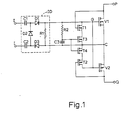
- MOS power transistors V1, V2 are connected, in reverse series across switch terminals P, Q.
- the gates and sources of the transistors are connected respectively to points G and C across which the drive signals from the isolation and drive circuit ID are connected.
- the transistor V1 When turned on by a positive potential applied at G, the transistor V1 will pass conventional current from P to Q, transistor V2 passing current by virtue of the inherent diode action of the VMOS transistor in the reverse direction.
- Two field-effect transistors T1, T2 have their drains connected to G, sources to C via T3 an T4 respectively, and their gates to P and Q respectively. Assuming for the present that T3 and T4 are in the 'on' state, in the event of a current surge through the switch, the voltage PC or QC rises: when its threshold voltage is exceeded, transistor T1 or T2 turns on, reducing the voltage GC to zero, and the switch turns off.
- the further transistors T3, T4, in series with transistors T1, T2, have their gate electrodes supplied from the control output of the drive circuit ID via an R-C circuit R2, C3.
- the R2/C3 element serves to delay the turn-on of transistors T3 and T4 on initial switch-on, ensuring that V1 and V2 are fully ON before the trip function is enabled.
- transistors T3 and T4 are also ON. In the event of a surge rendering transistor T1 (for example) conductive, the switch will turn off.
- the form of the isolation and drive circuit ID is not material to the present invention, and could take the form described in the above-mentioned paper. As shown, however, it comprises isolating capacitors C1, C2 (typically 15 pF), diodes D1, D2, D3 and resistor R1 to convert push-pull square waves at the input I to a dc control voltage; smoothing being effected by the inherent gate capacitance of the transistors V1, V2.
- the circuit shown is able to reset automatically when the off-state line voltage exceeds the threshold voltage, the switch is initially held off following the surge.
- Transistors T1 and T3 being turned on, however, permits the capacitor C3 to discharge via R2, turning transistor T3 off and thereby allowing transistor V1 to turn on again after a period-which might typically be 2 ms-determined by the time constant of C3/C2. If the surge persists beyond this period, the switch turns back on in a current-limit mode, returning to the fully-on state only when line conditions are normal.
- the gate-source voltages of T3 and V1 are the same and therefore the constant current passed by V1 will depend on the relative gate threshold voltages of these two transistors.
- the substrats of transistors T1 and T2 can either be connected as shown, or connected with those of the other transistors to point C.
- the gates of transistors T1, T2 are subject to the maximum voltages appearing on the line which for some applications will require fabrication of transistors with improved gate oxide isolation characteristics and/or unduly limit the maximum surge voltages that can be tolerated.
- the modified arrangement of Figure 2 is aimed at alleviating this problem. Instead of connecting the line terminal P directly to the gate of T1, a voltage-limiting arrangement is added, employing a series resistor R4 and a shunt arrangement consisting of a field-effect transistor T5 connected with pull-down resistor R6 in a constant voltage arrangement. A low voltage zener diode could be used, but the arrangement shown is simpler to implement in an integrated circuit.
- the control transistor T3 in the source circuit of T1 is replaced by a transistor T3' in series with resistor R4 so that the voltage-limiting arrangement draws no current when the switch is turned off.
- This also has the effect of facilitating the attainment of a higher current in the current limiting mode since the voltage applied to the gate of V1 in this mode is now the sum of the threshold voltages of T3' and T1, rather than merely that of T3 as is the case in Figure 1.
- An identical control arrangement, with transistors T4', T6 and resistors R5, R7, is provided for T2.
- a prototype circuit according to Figure 2 has been constructed having the following component values. and has 'ON' resistance of 19 0 with a trip current of 110 mA and a constant current of 16 mA in current limiting mode.
- the transistors are all n-channel enhancement types: obviously p-channel types could be employed, with appropriate reversal of the polarity of the drive signals from the isolation and drive circuit ID.
Landscapes
- Electronic Switches (AREA)
- Oscillators With Electromechanical Resonators (AREA)
- Air Bags (AREA)
Claims (9)
Priority Applications (1)
| Application Number | Priority Date | Filing Date | Title |
|---|---|---|---|
| AT84305174T ATE36790T1 (de) | 1983-08-10 | 1984-07-30 | Elektronischer schalter. |
Applications Claiming Priority (2)
| Application Number | Priority Date | Filing Date | Title |
|---|---|---|---|
| GB8321549 | 1983-08-10 | ||
| GB838321549A GB8321549D0 (en) | 1983-08-10 | 1983-08-10 | Electronic switch |
Publications (3)
| Publication Number | Publication Date |
|---|---|
| EP0133789A2 EP0133789A2 (de) | 1985-03-06 |
| EP0133789A3 EP0133789A3 (en) | 1985-04-10 |
| EP0133789B1 true EP0133789B1 (de) | 1988-08-24 |
Family
ID=10547117
Family Applications (1)
| Application Number | Title | Priority Date | Filing Date |
|---|---|---|---|
| EP84305174A Expired EP0133789B1 (de) | 1983-08-10 | 1984-07-30 | Elektronischer Schalter |
Country Status (5)
| Country | Link |
|---|---|
| US (1) | US4686383A (de) |
| EP (1) | EP0133789B1 (de) |
| AT (1) | ATE36790T1 (de) |
| DE (1) | DE3473707D1 (de) |
| GB (1) | GB8321549D0 (de) |
Families Citing this family (32)
| Publication number | Priority date | Publication date | Assignee | Title |
|---|---|---|---|---|
| SE453784B (sv) * | 1986-07-04 | 1988-02-29 | Ericsson Telefon Ab L M | Krets |
| SE455146B (sv) * | 1986-10-28 | 1988-06-20 | Ericsson Telefon Ab L M | Spenningsskyddskrets |
| US4853820A (en) * | 1987-05-11 | 1989-08-01 | Hendry Mechanical Works | Electronic circuit breaker systems |
| US4845388A (en) * | 1988-01-20 | 1989-07-04 | Martin Marietta Corporation | TTL-CMOS input buffer |
| FR2635930B1 (fr) * | 1988-08-31 | 1990-11-23 | Sgs Thomson Microelectronics | Commutateur bidirectionnel monolithique a transistors mos de puissance |
| US4924344A (en) * | 1989-02-27 | 1990-05-08 | Teledyne Industries, Inc. | Circuitry for protection against electromotively-induced voltage transients in solid state relay circuits |
| US4931778A (en) * | 1989-02-27 | 1990-06-05 | Teledyne Industries, Inc. | Circuitry for indicating the presence of an overload or short circuit in solid state relay circuits |
| US4916572A (en) * | 1989-02-27 | 1990-04-10 | Teledyne Industries, Inc. | Circuitry for protecting against load voltage transients in solid state relay circuits |
| US4916337A (en) * | 1989-03-07 | 1990-04-10 | Integrated Device Technology, Inc. | TTL to CMOS logic level translator |
| JPH079442B2 (ja) * | 1989-09-20 | 1995-02-01 | 株式会社東芝 | 電流検出回路 |
| US5049764A (en) * | 1990-01-25 | 1991-09-17 | North American Philips Corporation, Signetics Div. | Active bypass for inhibiting high-frequency supply voltage variations in integrated circuits |
| US5019720A (en) * | 1990-03-12 | 1991-05-28 | Ncr Corporation | Integrated circuit driver for serial bus having output overvoltage protection |
| US5193042A (en) * | 1990-12-07 | 1993-03-09 | Dielpromex S.A. De C.V. | Automatic energizing damping device |
| US5111067A (en) * | 1991-04-29 | 1992-05-05 | Intel Corporation | Power up reset circuit |
| US5142432A (en) * | 1991-10-21 | 1992-08-25 | General Motors Corporation | Fault detection apparatus for a transformer isolated transistor drive circuit for a power device |
| JP2814905B2 (ja) * | 1993-12-28 | 1998-10-27 | 日本電気株式会社 | ドライバ/レシーバ回路 |
| IE950365A1 (en) * | 1994-09-27 | 1996-04-03 | Armstrong Charles V | Power cut-off device |
| JPH0897362A (ja) * | 1994-09-28 | 1996-04-12 | Nittetsu Semiconductor Kk | 半導体集積回路の電源保護回路 |
| US5729236A (en) * | 1995-04-28 | 1998-03-17 | Texas Instruments Incorporated | Identification system reader with multiplexed antennas |
| US5801561A (en) * | 1995-05-01 | 1998-09-01 | Intel Corporation | Power-on initializing circuit |
| US5541881A (en) * | 1995-06-07 | 1996-07-30 | International Business Machines Corporation | High gain feedback latch |
| US5745323A (en) * | 1995-06-30 | 1998-04-28 | Analog Devices, Inc. | Electrostatic discharge protection circuit for protecting CMOS transistors on integrated circuit processes |
| US5943203A (en) * | 1997-09-12 | 1999-08-24 | Linfinity Microelectronics Inc. | Electronic circuit breaker |
| US6153948A (en) * | 1998-08-13 | 2000-11-28 | Cogan; Adrian I. | Electronic circuits with wide dynamic range of on/off delay time |
| CA2360117A1 (en) * | 2001-10-24 | 2003-04-24 | Catena Networks Canada Inc. | The application of pots ringing signals without interfering with dsl signals |
| US7369385B2 (en) * | 2002-07-09 | 2008-05-06 | Analog Devices, Inc. | Overload limiting circuit |
| AU2002950581A0 (en) * | 2002-08-02 | 2002-09-12 | Wayne Callen | Electrical safety circuit |
| JP2007228447A (ja) * | 2006-02-27 | 2007-09-06 | Hitachi Ltd | スイッチング素子のゲート駆動回路 |
| US8760827B2 (en) * | 2009-04-15 | 2014-06-24 | International Business Machines Corporation | Robust ESD protection circuit, method and design structure for tolerant and failsafe designs |
| US9755630B2 (en) * | 2009-04-30 | 2017-09-05 | The United States of America as represented by the Secretary of the Government | Solid-state circuit breakers and related circuits |
| US8710541B2 (en) * | 2012-03-20 | 2014-04-29 | Analog Devices, Inc. | Bi-directional switch using series connected N-type MOS devices in parallel with series connected P-type MOS devices |
| US10122359B2 (en) * | 2015-08-07 | 2018-11-06 | Semiconductor Components Industries, Llc | Integrated circuit control of anti-series switches |
Family Cites Families (21)
| Publication number | Priority date | Publication date | Assignee | Title |
|---|---|---|---|---|
| US3970869A (en) * | 1975-03-03 | 1976-07-20 | The United States Of America As Represented By The Secretary Of The Navy | Low power driver |
| FR2351545A1 (fr) * | 1976-05-10 | 1977-12-09 | Telemecanique Electrique | Commutateur a transistors, muni d'un dispositif de protection contre les surintensites, avec rearmement automatique |
| US4090227A (en) * | 1977-03-29 | 1978-05-16 | Bell Telephone Laboratories, Incorporated | Transient-protected signal distribution circuit |
| FR2458180A2 (fr) * | 1979-05-30 | 1980-12-26 | Telemecanique Electrique | Commutateur a transistors, muni d'un dispositif de protection contre les surintensites, avec rearmement automatique |
| US4363068A (en) * | 1980-08-18 | 1982-12-07 | Sundstrand Corporation | Power FET short circuit protection |
| DE3034927C2 (de) * | 1980-09-16 | 1983-09-22 | Siemens AG, 1000 Berlin und 8000 München | Schaltungsanordnung zum Schutz eines Leistungs-MOSFET gegen Überlastung |
| DE3108385C2 (de) * | 1981-03-05 | 1982-12-02 | Siemens AG, 1000 Berlin und 8000 München | Verfahren zur Ansteuerung eines Leistungs-Feldeffekt-Schalttransistors und Schaltungsanordnungen zur Durchführung des Verfahrens |
| JPS58116759A (ja) * | 1981-12-29 | 1983-07-12 | Fujitsu Ltd | 出力ドライバ回路 |
| DE3202319A1 (de) * | 1982-01-26 | 1983-07-28 | Siemens AG, 1000 Berlin und 8000 München | Schutzschaltung fuer einen leistungstransistor |
| US4424544A (en) * | 1982-02-09 | 1984-01-03 | Bell Telephone Laboratories, Incorporated | Optically toggled bidirectional switch |
| US4438356A (en) * | 1982-03-24 | 1984-03-20 | International Rectifier Corporation | Solid state relay circuit employing MOSFET power switching devices |
| JPS58164323A (ja) * | 1982-03-25 | 1983-09-29 | Nissan Motor Co Ltd | 半導体スイツチ回路 |
| US4481553A (en) * | 1982-04-05 | 1984-11-06 | General Electric Company | Protection circuit |
| JPS58178632A (ja) * | 1982-04-13 | 1983-10-19 | Nissan Motor Co Ltd | スイツチ回路 |
| US4500801A (en) * | 1982-06-21 | 1985-02-19 | Eaton Corporation | Self-powered nonregenerative fast gate turn-off FET |
| US4429339A (en) * | 1982-06-21 | 1984-01-31 | Eaton Corporation | AC Transistor switch with overcurrent protection |
| US4491750A (en) * | 1982-09-28 | 1985-01-01 | Eaton Corporation | Bidirectionally source stacked FETs with drain-referenced common gating |
| DE3243467C2 (de) * | 1982-11-24 | 1986-02-20 | Siemens AG, 1000 Berlin und 8000 München | Einrichtung zum Schutz eines Schalttransistors |
| US4513341A (en) * | 1983-07-25 | 1985-04-23 | Gte Lenkurt Incorporated | Overvoltage protection circuit for power supply |
| DE3338124A1 (de) * | 1983-10-20 | 1985-05-02 | Telefunken electronic GmbH, 7100 Heilbronn | Stoerschutzschaltung fuer integrierte schaltungen |
| US4581540A (en) * | 1984-03-16 | 1986-04-08 | Teledyne Industries, Inc. | Current overload protected solid state relay |
-
1983
- 1983-08-10 GB GB838321549A patent/GB8321549D0/en active Pending
-
1984
- 1984-07-30 EP EP84305174A patent/EP0133789B1/de not_active Expired
- 1984-07-30 AT AT84305174T patent/ATE36790T1/de active
- 1984-07-30 DE DE8484305174T patent/DE3473707D1/de not_active Expired
- 1984-08-10 US US06/639,328 patent/US4686383A/en not_active Expired - Fee Related
Also Published As
| Publication number | Publication date |
|---|---|
| EP0133789A3 (en) | 1985-04-10 |
| ATE36790T1 (de) | 1988-09-15 |
| GB8321549D0 (en) | 1983-09-14 |
| DE3473707D1 (en) | 1988-09-29 |
| EP0133789A2 (de) | 1985-03-06 |
| US4686383A (en) | 1987-08-11 |
Similar Documents
| Publication | Publication Date | Title |
|---|---|---|
| US4686383A (en) | Electronic switch with automatic protective turn-off followed by automatic reset | |
| US5087871A (en) | Power supply with inrush current limiter | |
| US4438356A (en) | Solid state relay circuit employing MOSFET power switching devices | |
| KR950009087B1 (ko) | 반도체 집적회로의 출력회로 | |
| US4409501A (en) | Power-on reset circuit | |
| US5272399A (en) | Circuit limiting the load current of a power MOSFET | |
| US20030090158A1 (en) | System and method for redundant power supply connection | |
| JP3547135B2 (ja) | 電界効果トランジスタを用いた保護デバイス | |
| US5886556A (en) | Low power schmitt trigger | |
| US4581545A (en) | Schmitt trigger circuit | |
| US4575642A (en) | Control circuit for an integrated device | |
| US6703889B2 (en) | In-rush current protection | |
| JPH09181588A (ja) | 半導体スイッチ | |
| AU4591099A (en) | High voltage protection circuit on standard cmos process | |
| US6067219A (en) | Power cut-off device | |
| GB2473516A (en) | Transient blocking unit with an enhancement mode device in the current path | |
| JPS58130726A (ja) | パワ−トランジスタの保護回路 | |
| US3448293A (en) | Field effect switching circuit | |
| EP1100200B1 (de) | Analogschalter mit zwei komplementären MOS-Feldeffekttransistoren | |
| CN1089403A (zh) | 开关装置 | |
| US4408137A (en) | Break-before-make solid state relay | |
| US5914628A (en) | Circuit for controlling a triac at the voltage zero | |
| EP0084721A1 (de) | Festkörperrelais | |
| US6020779A (en) | Electrical switching device with control signal input | |
| EP0669718A1 (de) | Elektronischer Schalter für integrierte MOS-Schaltungen mit niedriger Versorgungsspannung |
Legal Events
| Date | Code | Title | Description |
|---|---|---|---|
| PUAI | Public reference made under article 153(3) epc to a published international application that has entered the european phase |
Free format text: ORIGINAL CODE: 0009012 |
|
| PUAL | Search report despatched |
Free format text: ORIGINAL CODE: 0009013 |
|
| AK | Designated contracting states |
Designated state(s): AT BE CH DE FR GB IT LI LU NL SE |
|
| AK | Designated contracting states |
Designated state(s): AT BE CH DE FR GB IT LI LU NL SE |
|
| 17P | Request for examination filed |
Effective date: 19850813 |
|
| 17Q | First examination report despatched |
Effective date: 19860828 |
|
| D17Q | First examination report despatched (deleted) | ||
| RAP1 | Party data changed (applicant data changed or rights of an application transferred) |
Owner name: BRITISH TELECOMMUNICATIONS PUBLIC LIMITED COMPANY |
|
| GRAA | (expected) grant |
Free format text: ORIGINAL CODE: 0009210 |
|
| AK | Designated contracting states |
Kind code of ref document: B1 Designated state(s): AT BE CH DE FR GB IT LI LU NL SE |
|
| REF | Corresponds to: |
Ref document number: 36790 Country of ref document: AT Date of ref document: 19880915 Kind code of ref document: T |
|
| ITF | It: translation for a ep patent filed | ||
| REF | Corresponds to: |
Ref document number: 3473707 Country of ref document: DE Date of ref document: 19880929 |
|
| ET | Fr: translation filed | ||
| PLBE | No opposition filed within time limit |
Free format text: ORIGINAL CODE: 0009261 |
|
| STAA | Information on the status of an ep patent application or granted ep patent |
Free format text: STATUS: NO OPPOSITION FILED WITHIN TIME LIMIT |
|
| 26N | No opposition filed | ||
| BECN | Be: change of holder's name |
Effective date: 19880824 |
|
| PGFP | Annual fee paid to national office [announced via postgrant information from national office to epo] |
Ref country code: GB Payment date: 19900608 Year of fee payment: 7 |
|
| PGFP | Annual fee paid to national office [announced via postgrant information from national office to epo] |
Ref country code: BE Payment date: 19900628 Year of fee payment: 7 |
|
| PGFP | Annual fee paid to national office [announced via postgrant information from national office to epo] |
Ref country code: SE Payment date: 19900711 Year of fee payment: 7 |
|
| PGFP | Annual fee paid to national office [announced via postgrant information from national office to epo] |
Ref country code: FR Payment date: 19900719 Year of fee payment: 7 |
|
| PGFP | Annual fee paid to national office [announced via postgrant information from national office to epo] |
Ref country code: CH Payment date: 19900724 Year of fee payment: 7 |
|
| PGFP | Annual fee paid to national office [announced via postgrant information from national office to epo] |
Ref country code: AT Payment date: 19900730 Year of fee payment: 7 |
|
| ITTA | It: last paid annual fee | ||
| PGFP | Annual fee paid to national office [announced via postgrant information from national office to epo] |
Ref country code: NL Payment date: 19900731 Year of fee payment: 7 |
|
| PGFP | Annual fee paid to national office [announced via postgrant information from national office to epo] |
Ref country code: DE Payment date: 19900828 Year of fee payment: 7 |
|
| PGFP | Annual fee paid to national office [announced via postgrant information from national office to epo] |
Ref country code: LU Payment date: 19910703 Year of fee payment: 8 |
|
| PG25 | Lapsed in a contracting state [announced via postgrant information from national office to epo] |
Ref country code: GB Effective date: 19910730 Ref country code: AT Effective date: 19910730 |
|
| PG25 | Lapsed in a contracting state [announced via postgrant information from national office to epo] |
Ref country code: SE Effective date: 19910731 Ref country code: LI Effective date: 19910731 Ref country code: CH Effective date: 19910731 Ref country code: BE Effective date: 19910731 |
|
| EPTA | Lu: last paid annual fee | ||
| BERE | Be: lapsed |
Owner name: BRITISH TELECOMMUNICATIONS PLC Effective date: 19910731 |
|
| PG25 | Lapsed in a contracting state [announced via postgrant information from national office to epo] |
Ref country code: NL Effective date: 19920201 |
|
| NLV4 | Nl: lapsed or anulled due to non-payment of the annual fee | ||
| GBPC | Gb: european patent ceased through non-payment of renewal fee | ||
| PG25 | Lapsed in a contracting state [announced via postgrant information from national office to epo] |
Ref country code: FR Effective date: 19920331 |
|
| REG | Reference to a national code |
Ref country code: CH Ref legal event code: PL |
|
| PG25 | Lapsed in a contracting state [announced via postgrant information from national office to epo] |
Ref country code: DE Effective date: 19920401 |
|
| REG | Reference to a national code |
Ref country code: FR Ref legal event code: ST |
|
| PG25 | Lapsed in a contracting state [announced via postgrant information from national office to epo] |
Ref country code: LU Free format text: LAPSE BECAUSE OF NON-PAYMENT OF DUE FEES Effective date: 19920730 |
|
| EUG | Se: european patent has lapsed |
Ref document number: 84305174.9 Effective date: 19920210 |