EP0134432B1 - Cicuit intégré semi-conducteur complémentaire comportant un dispositif de protection - Google Patents
Cicuit intégré semi-conducteur complémentaire comportant un dispositif de protection Download PDFInfo
- Publication number
- EP0134432B1 EP0134432B1 EP84106779A EP84106779A EP0134432B1 EP 0134432 B1 EP0134432 B1 EP 0134432B1 EP 84106779 A EP84106779 A EP 84106779A EP 84106779 A EP84106779 A EP 84106779A EP 0134432 B1 EP0134432 B1 EP 0134432B1
- Authority
- EP
- European Patent Office
- Prior art keywords
- impurity region
- field effect
- effect transistor
- insulated gate
- gate field
- Prior art date
- Legal status (The legal status is an assumption and is not a legal conclusion. Google has not performed a legal analysis and makes no representation as to the accuracy of the status listed.)
- Expired
Links
- 239000004065 semiconductor Substances 0.000 title claims description 33
- 230000000295 complement effect Effects 0.000 title 1
- 239000000758 substrate Substances 0.000 claims description 29
- 239000012535 impurity Substances 0.000 claims description 28
- 230000005669 field effect Effects 0.000 claims description 14
- 238000002955 isolation Methods 0.000 claims description 3
- 230000015556 catabolic process Effects 0.000 description 46
- 238000009792 diffusion process Methods 0.000 description 26
- 230000000694 effects Effects 0.000 description 14
- 239000012212 insulator Substances 0.000 description 6
- 238000010586 diagram Methods 0.000 description 5
- 238000009413 insulation Methods 0.000 description 4
- 229910021420 polycrystalline silicon Inorganic materials 0.000 description 4
- 229920005591 polysilicon Polymers 0.000 description 4
- 229910052751 metal Inorganic materials 0.000 description 3
- 239000002184 metal Substances 0.000 description 3
- 229910052782 aluminium Inorganic materials 0.000 description 2
- XAGFODPZIPBFFR-UHFFFAOYSA-N aluminium Chemical compound [Al] XAGFODPZIPBFFR-UHFFFAOYSA-N 0.000 description 2
- 239000000470 constituent Substances 0.000 description 2
- 238000010276 construction Methods 0.000 description 2
- 230000006870 function Effects 0.000 description 2
- 239000000463 material Substances 0.000 description 2
- 238000005259 measurement Methods 0.000 description 2
- 230000003071 parasitic effect Effects 0.000 description 2
- 239000002131 composite material Substances 0.000 description 1
- 230000003247 decreasing effect Effects 0.000 description 1
- 230000005684 electric field Effects 0.000 description 1
- 230000036039 immunity Effects 0.000 description 1
- 230000004048 modification Effects 0.000 description 1
- 238000012986 modification Methods 0.000 description 1
- 230000008054 signal transmission Effects 0.000 description 1
- 229910021332 silicide Inorganic materials 0.000 description 1
- FVBUAEGBCNSCDD-UHFFFAOYSA-N silicide(4-) Chemical compound [Si-4] FVBUAEGBCNSCDD-UHFFFAOYSA-N 0.000 description 1
Images



Classifications
-
- H—ELECTRICITY
- H10—SEMICONDUCTOR DEVICES; ELECTRIC SOLID-STATE DEVICES NOT OTHERWISE PROVIDED FOR
- H10D—INORGANIC ELECTRIC SEMICONDUCTOR DEVICES
- H10D30/00—Field-effect transistors [FET]
- H10D30/60—Insulated-gate field-effect transistors [IGFET]
-
- H—ELECTRICITY
- H10—SEMICONDUCTOR DEVICES; ELECTRIC SOLID-STATE DEVICES NOT OTHERWISE PROVIDED FOR
- H10D—INORGANIC ELECTRIC SEMICONDUCTOR DEVICES
- H10D89/00—Aspects of integrated devices not covered by groups H10D84/00 - H10D88/00
- H10D89/60—Integrated devices comprising arrangements for electrical or thermal protection, e.g. protection circuits against electrostatic discharge [ESD]
- H10D89/601—Integrated devices comprising arrangements for electrical or thermal protection, e.g. protection circuits against electrostatic discharge [ESD] for devices having insulated gate electrodes, e.g. for IGFETs or IGBTs
- H10D89/811—Integrated devices comprising arrangements for electrical or thermal protection, e.g. protection circuits against electrostatic discharge [ESD] for devices having insulated gate electrodes, e.g. for IGFETs or IGBTs using FETs as protective elements
-
- H—ELECTRICITY
- H10—SEMICONDUCTOR DEVICES; ELECTRIC SOLID-STATE DEVICES NOT OTHERWISE PROVIDED FOR
- H10D—INORGANIC ELECTRIC SEMICONDUCTOR DEVICES
- H10D84/00—Integrated devices formed in or on semiconductor substrates that comprise only semiconducting layers, e.g. on Si wafers or on GaAs-on-Si wafers
Definitions
- This invention relates generally to a semiconductor device and more particularly, to a protection device in a metal insulator semiconductor (MIS) device such as an insulated gate field effect transistor (hereinafter called a "MOS transistor").
- MIS metal insulator semiconductor
- MOS transistor insulated gate field effect transistor
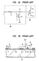
- reference numeral 1 represents an input terminal
- reference numeral 2 does a clamp resistance which is ordinarily composed of a diffusion layer or a polysilicon layer.
- Reference numeral 3 represents a surface breakdown type MOS transistor having the gate 4 thereof kept at a ground potential, and reference numeral 5 represents its drain.
- the drain terminal 5 is connected to the gate terminal 6 of a MOS transistor to be protected.
- an electric field crowds between the drain and the gate and finally, electrical breakdown occurs at the surface of the semi- conductor substrate under the gate of the MOS transistor. After the breakdown, the current flows from the drain 5 to the ground through the substrate, and is limited by the resistance of the substrate.
- Reference numerals 8 and 9 represent the drain and source of a MOS transistor 7. Generally, the surface breakdown voltage of the MOS transistor 3 is about 15V.
- Figure 1 B shows the sectional structure of the protection device 101 shown in Figure 1A.
- reference numeral 10 represents a p-type substrate
- 12 is the input terminal 1 in Figure 1A
- 102 is a clamp resistance formed by n + diffusion.
- the MOS transistor represented by reference numeral 3 has a gate 17 consisting of polysilicon and drain and source consisting of n +- type diffusion layers 15, 16. The members 17 and 16 are connected to the ground 18 while the member 1.5 is connected to the output 14 of a diffusion resistance 102, and hence to the gate of the active MOS device.
- Reference numeral 19 represents the gate oxide of the MOS transistor 3, and its structure and thickness are the same as those of the gate oxide of the active MOS device.
- Reference numeral 11 represents a thick insulation film for separating the devices.
- the operation of the protection device will be explained about the case in which the gate oxide film 19 is 50 nm thick, the breakdown voltage of the oxide film is 25V, the surface breakdown voltage of the MOS transistor 3 is 15V, a supply voltage of 5V is applied to the drain 8 of the active MOS transistor 7, and its source is at the ground potential.
- the MOS transistor 3 When a positive voltage is applied to the input terminal 1 and the voltage at the input terminal 5 of the active MOS device is above 15V, the MOS transistor 3 undergoes breakdown, and a current flows through the ground terminal. If the resistance is 100 Ohms and the resistance 2 is 2 K Ohms after this breakdown, the voltage at which the gate insulation film of the active MOS device undergoes breakdown, that is, the input terminal voltage at which the voltage of the terminal 5 reaches 25 V, is found to be about 220 V by measurement.
- the p-type substrate 10 and the n +- type diffusion layer 102 are in the diode connection in the forward direction if the p-type substrate 10 is at the ground potential, and a voltage above about a constant voltage of -0.6 V is not applied to the gate oxide film 19.
- the protection device of the prior art exhibits its effect in that the breakdown of the gate insulation film of the active MOS device is prevented.
- it is used actually as one of the constituents for an IC (integrated circuit) or an LSI (large scale integrated circuit), however, various problems are encountered.
- the first problem is as follows.
- the clamp resistance 2 is made of the same n +- type diffusion layer as that forming the drain and source of the active MOS device, and its value is kept as low as possible in order not to deteriorate various characteristics of the active MOS device.
- the value of the clamp resistance 2 is increased, therefore, the area of the resistance itself becomes great.
- the second problem is as follows.
- An external clock signal is applied to the input terminal 1 or to the input terminal 20 in Figure 2.
- a signal having a TTL (Transistbr-Transistor Logic) level or a low level of from 0 to 0.8 V and a high level of from 2.2 to 5 V is applied.
- a clock pulse having a voltage swing whose low level is below 0 V, e.g., from about -3 to about -5 V, and is below the potential (0 V) of the substrate (10, (clock signal having so-called “under-shoot") is applied from time to time depending upon the kind of the system to be employed.
- a parasitic bipolar device which uses the source or drain formed by the n +- type diffusion layer of the active MOS device as its collector, the p-type substrate as its base, and the resistance formed by the n +- type diffusion layer as its emitter, operates, though only temporarily. If the active device is one of the elements of memory cells and the drain forms a storage node in this case, the stored data are destroyed.
- the active circuit 102 consists of a p-channel MOS transistor 44 whose source and drain are formed by the p-type diffusion layers 29, 30 and whose gate is represented by reference numeral 33, and an n-channel MOS transistor 45 whose drain and source are formed by the n-type diffusion layers 26, 27 and whose gate is represented by reference numeral 34.
- the p-type well 36 is kept fixed at the ground potential through the p-type diffusion layer 31 together with the source 27, while the n-type substrate 37 is kept fixed at a power source (V cc ) potential through the n-type diffusion layer 25 together with the source 29, with their drains 30 and 26 being connected to each other to form a so-called "CMOS inverter circuit".
- Reference numeral 38 represents the gate insulator film (e.g., oxide film) of the MOS transistor 43, and its structure and thickness are the same as those of the gate insulator films 39, 40 of the active MOS transistors.
- the concentration and depth of the p-type well 35 are also the same as those of the p-type well 36 of the active MOS transistor 45.
- the gate oxide films 38, 39 and 40 are 50 nm thick, their breakdown voltage is 25 V, the surface breakdown voltage of the MOS transistor 43 formed by the drain 23, source 24 and gate 32 is 15 V, a power source voltage of 5 V is applied to the drain 41 of the active MOS transistor 45 and its source 27 is at the ground potential.
- the MOS transistor 43 undergoes breakdown, and a current flows through the ground terminal. If the resistance is 100 Ohms and the value of the clamp resistance 21 is 2 K Ohms after this breakdown, the voltage at which the gate of the active MOS transistor undergoes breakdown, that is, the value of the input terminal voltage necessary for the voltage of the terminal 22 to rise to 25 V, is found to be about 220 V by measurement.
- the member 35 and the +- type diffusion layer 23 are in the diode connection in the forward direction if the p-type well 35 is at the ground potential, and a voltage above a constant voltage of about -0.6 V is not applied to the gate oxide films 39, 40 of the transistors 44, 45.
- the protection device shown in Figure 2 exhibits its effect in that it prevents the breakdown of the gate insulator film of the active MOS transistor.
- the protection device shown in Figure 2 When it is used in practice as one of the elements of an IC or an LSI, however, the following various problems are encountered.
- the first problem is as follows.
- the gate insulator film must essentially be made thinner in order to sufficiently improve the transistor characteristics but along therewith, the voltage value at which the gate of the active MOS transistor undergoes breakdown also drops.
- the gate oxide film is made thinner, the surface breakdown voltage of the MOS transistor 43 tends to reduce and contributes to improve the breakdown voltage of the gate oxide film.
- the value of the breakdown voltage of the gate oxide film as viewed from the input terminal is lower than that of the prior art.
- the second problem is as follows. High speed performance has been required recently for ICs and LSls using MOS transistors, and examination has been made to improve the high speed performance of active circuits. In this sense, the delay time of R-C consisting of parasitic capacitance of the clamp resistance 21 and a wiring 22 interposed between the input terminal 20 and the transistor 43 has become a critical problem. When the value of the breakdown voltage of the gate oxide film as viewed from then input terminal is to be increased, the value of the clamp resistance 21 must be increased unavoidably, so that the delay time becomes greater and the high speed performance of the circuit is lost.
- the fundamental concept of the present invention is as follows.
- the present invention pays specific attention to a surface breakdown type MOS transistor (MOS transistor 43 in Figure 2) forming the protection device, and drastically improves the gate breakdown voltage, as viewed from the input terminal, by reducing the breakdown voltage of the MOS transistor and reducing the resistance after the breakdown.
- the object described above can be accomplished by increasing the concentration of the region, where the surface breakdown type MOS transistor is to be disposed, and or decreasing its depth to be thinner than the depth of the region, where the active MOS transistor is to be disposed.
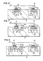
- Figure 3 shows the cross-sectional structure of a semiconductor device in accordance with the first embodiment of the present invention.
- reference numeral 50 represents a p-type well
- reference numeral 51 does a signal transmission terminal (internal terminal) through a resistance.
- Like reference numerals are used to identify the other constituents which are the same as, or analogous to, those in Figure 2.
- the channel MOS transistor 44 is omitted from the drawing, but it is disposed in practice inside the n-type substrate 37 as shown in Figure 2.
- the characterizing feature of this embodiment resides in that the MOS transistor represented by 43 in Figure 2 is disposed inside the p-type well represented by 50 in Figure 3. Unlike the p-type wells 35 and 36 shown in Figure 2, the carrier concentration of this p-type well 50 is by about five to ten times higher, and the sheet resistance is also lower. When the carrier concentration of the substrate is about 10 15 /cm 3 , for example, the carrier concentration of the region 36 is from about -1015 to about 10 16 /cm 3 , and that of the region 50, at least 10 17 /cm 3 .
- Figure 4 shows the characteristics of surface breakdown of the two MOS transistors 43 ( Figures 2 and 3) formed inside the p-type well represented by 35 or 36 and inside the p-type well represented by 50, respectively.
- 4A CONVENTIONAL
- 4B PROPOSED
- 4A represents the breakdown characteristics of the MOS transistor 43 ( Figure 2) formed inside the conventional p-type well 35 or 36
- 4B PROPOSED
- 4A represents the breakdown characteristics of the MOS transistor 43 formed inside the p-type well 50 in accordance with the present invention.
- the surface breakdown voltage of the MOS transistor in accordance with the present invention exhibits the voltage drop of at least 5 V in comparison with the conventional transistor, and the value of the internal resistance bcomes extremely small due to the rise characteristics of the current characteristics.
- Figure 5 shows the withstand voltage of the transistor with respect to the input voltage, and is a modification of Figure 4.
- Figure 5 shows the relation between the input voltage and the output voltage (51 in Figure 3) through the protection circuit (with the clamp resistance being as shown in Figure 2).
- the voltage of 51 is proportional to the input voltage till the MOS transistor 43 undergoes breakdown, but after the breakdown, it rises at a ratio of the resistances between the clamp resistance and the internal resistance of breakdown.
- the breakdown voltage value (at point 5A) as well as the internal resistance value after the breakdown are high, so that the gradient with respect to the input terminal voltage is also high (5a).
- the breakdown voltage value is small (5B) and the internal resistance is also small (5b), so that the value of the input terminal voltage before the voltage V B at which the gate oxide film of the active circuit undergoes breakdown, can be drastically increased when compared with the prior art devices.
- the effect of the present invention described above means also the following.
- the value of the input terminal voltage before the voltage V B at which the gate oxide film of the active circuit undergoes breakdown, has a sufficiently large margin in comparison with the prior art, so that the value of the input clamp resistance can be further reduced. Needless to say, this provides a great advantage for ICs and LSIs with shorter delay time.
- Figure 6 shows the sectional structure of the semiconductor device in accordance with the second embodiment of the present invention.
- the MOS transistor 43 is shown formed inside a p-type well 60 whose carrier concentration is by about five to ten times higher than that of the p-type well 36 forming the active MOS transistor 45 and whose depth is smaller than the latter.
- the well 36 is at least 3 um whereas the well 60 is up to 3 g m, for example, and this embodiment provides the same effect as that of the first embodiment shown in Figure 3. Moreover, this embodiment provides the following effect.
- the p-type well 60 is shallow, the p-type well region below the N diffusion layer 23 is completely depleted and so-called "punch-through" occurs when the voltage of the internal terminal 51, that is, the terminal voltage of the N + diffusion layer 23, reaches a predetermined voltage with the n-type substrate 37 being at the ground potential.
- punch-through takes place, the charge stored in the N + diffusion layer 23 flows to the substrate 37, with the result that the voltage rise of 51 is limited and the value of the breakdown voltage of the gate oxide film as viewed from the input terminal can be improved.
- an N-/N' epitaxial substrate is preferably used as the substrate 37.
- a higher effect could be obtained with a thinner N- layer forming the MOS transistor, and the N + layer, too, is preferably kept fixed at a predetermined potential from the reverse of the substrate through a metal.
- the carrier concentration of the p-type well 60 is increased and its depth is reduced, but the effect of the present invention can be obtained by reducing the depth of the well even when the concentration is the same.
- Figure 7 shows the cross-sectional structure of a semiconductor device in accordance with the third embodiment of the present invention.
- a p-type impurity layer 70 for keeping a p-type well 60 fixed at the ground potential is sufficiently spaced apart from layers forming a MOS transistor 43, such as a drain 23 and a source 24, for example.
- the member represented by reference numeral 70 is spaced apart from the member representdd by reference numeral 24. More definitely, it is preferably spaced apart in a distance exceeding the depths of the drain 23 and source 24.
- the holes are injected into the p-type well 60 and raises partially the potential under the MOS transistor 32, so that an NPN bipolar transistor using the n-type impurity layer 23 as the collector, the well 60 as the base and the n-type impurity layer 24 as the emitter operates.
- a large current can be caused to flow from 51 to the ground 701 through the bulk below the surface of the MOS transistor, and the protection effect can be further improved.
- Figure 8 shows the cross-sectional structure of a semiconductor device in accordance with the fourth embodiment of the present invention.
- this embodiment disposes a p-type well 80 which is analogous to the p-type well 36 forming the internal circuit.
- This embodiment provides the same effect as the third embodiment described above in the respect of the protection function of the breakdown of the internal gate, but in this embodiment, good immunity for a latch-up phenomenon (or thyristor effect), which occurs during normal operation and is inherent to the CMOS structure, can be obtained.
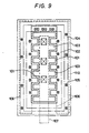
- Figure 9 shows the pattern layout of the semi- conductor device in accordance with the third embodiment of the present invention.
- reference numeral 107 represents the input terminal, which is an aluminum layer corresponding to the member 51 in Figure 7.
- Reference numeral 106 represents a ground terminal which is also an aluminum layer
- reference numerals 102 and 103 represents n-type diffusion layer regions which are source and drain, respectively.
- Reference numeral 101 represents a region which is to serve as the gate of an MOS transistor, and consists of a polysilicon layer, a silicide layer or a metal layer or a composite layer of them.
- Reference numeral 104 represents a p-type diffusion layer-forming region, which keeps a p-type well region 110 fixed at the ground potential.
- Reference numeral 105 represents a through-hole portion for connecting the diffusion layer of the gate layer.
- the gate layer has a large number of rectangular shapes so as to cause a large current to flow with a limited area. (The current can be increased by expanding the channel width.)
- Figure 10 shows the cross-sectional structure of a semiconductor device in accordance with the fifth embodiment of the present invention.
- this embodiment employs a structure in which a deep isolation 203 encompasses the protection circuit portion.
- Reference numeral 201 in the drawings represent an n-type semi-conductor layer
- 202 is an n +- type semiconductor layer having a lower resistance than that of the semi- conductor layer 201.
- This embodiment can completely prevent the latch-up phonemenon inherent to the CMOS structure described with reference. to Figure 8, and a protection circuit highly and really resistant to external noise can be obtained.
- An n +- or p-type diffusion layer, an insulator layer such as Si0 2 , a polysilicon layer, or the like, is used as the deep isolation 203.
- the present invention can provide a protection device which can eliminate the problems with the prior art.
- the input clamp resistance is not discussed, in particular, but it is obvious that the protection effect can be further improved by jointly using the input clamp resistance with the semiconductor device of the invention.
- the resistance material in this case may be the same that is used for the gate of the MOS transistor, and may be simultaneously formed with the gate. Alternatively, it may be a material that is fitted separately.
Landscapes
- Metal-Oxide And Bipolar Metal-Oxide Semiconductor Integrated Circuits (AREA)
- Insulated Gate Type Field-Effect Transistor (AREA)
- Semiconductor Integrated Circuits (AREA)
Claims (7)
Applications Claiming Priority (2)
| Application Number | Priority Date | Filing Date | Title |
|---|---|---|---|
| JP58107678A JPS60767A (ja) | 1983-06-17 | 1983-06-17 | 半導体装置 |
| JP107678/83 | 1983-06-17 |
Publications (3)
| Publication Number | Publication Date |
|---|---|
| EP0134432A2 EP0134432A2 (fr) | 1985-03-20 |
| EP0134432A3 EP0134432A3 (en) | 1985-10-23 |
| EP0134432B1 true EP0134432B1 (fr) | 1989-09-13 |
Family
ID=14465201
Family Applications (1)
| Application Number | Title | Priority Date | Filing Date |
|---|---|---|---|
| EP84106779A Expired EP0134432B1 (fr) | 1983-06-17 | 1984-06-14 | Cicuit intégré semi-conducteur complémentaire comportant un dispositif de protection |
Country Status (5)
| Country | Link |
|---|---|
| US (1) | US4616243A (fr) |
| EP (1) | EP0134432B1 (fr) |
| JP (1) | JPS60767A (fr) |
| KR (1) | KR920003676B1 (fr) |
| DE (1) | DE3479771D1 (fr) |
Families Citing this family (26)
| Publication number | Priority date | Publication date | Assignee | Title |
|---|---|---|---|---|
| JPS6132464A (ja) * | 1984-07-24 | 1986-02-15 | Nec Corp | Cmos型集積回路装置 |
| JPS61111576A (ja) * | 1984-10-13 | 1986-05-29 | Fujitsu Ltd | 半導体装置 |
| JPH0793360B2 (ja) * | 1985-10-18 | 1995-10-09 | 株式会社日立製作所 | 半導体素子 |
| US4821096A (en) * | 1985-12-23 | 1989-04-11 | Intel Corporation | Excess energy protection device |
| US5060037A (en) * | 1987-04-03 | 1991-10-22 | Texas Instruments Incorporated | Output buffer with enhanced electrostatic discharge protection |
| JPH01194349A (ja) * | 1988-01-29 | 1989-08-04 | Toshiba Corp | 半導体装置 |
| US5182621A (en) * | 1988-06-14 | 1993-01-26 | Nec Corporation | Input protection circuit for analog/digital converting semiconductor |
| JPH0298168A (ja) * | 1988-10-04 | 1990-04-10 | Nec Corp | 半導体装置 |
| JP2754072B2 (ja) * | 1990-02-07 | 1998-05-20 | 三菱電機株式会社 | 半導体装置の入力回路 |
| US5436183A (en) * | 1990-04-17 | 1995-07-25 | National Semiconductor Corporation | Electrostatic discharge protection transistor element fabrication process |
| US5021853A (en) * | 1990-04-27 | 1991-06-04 | Digital Equipment Corporation | N-channel clamp for ESD protection in self-aligned silicided CMOS process |
| JP3199808B2 (ja) * | 1991-05-14 | 2001-08-20 | セイコーインスツルメンツ株式会社 | 半導体集積回路装置 |
| JP3036905B2 (ja) * | 1991-06-28 | 2000-04-24 | 日本電気株式会社 | 相補型mis半導体装置 |
| JPH05109990A (ja) * | 1991-10-15 | 1993-04-30 | Nec Corp | 半導体集積回路装置 |
| US5371395A (en) * | 1992-05-06 | 1994-12-06 | Xerox Corporation | High voltage input pad protection circuitry |
| US5428498A (en) * | 1992-09-28 | 1995-06-27 | Xerox Corporation | Office environment level electrostatic discharge protection |
| DE4334515C1 (de) * | 1993-10-09 | 1994-10-20 | Itt Ind Gmbh Deutsche | Verpolungsschutz für integrierte elektronische Schaltkreise in CMOS-Technik |
| DE4423733C2 (de) * | 1994-07-06 | 1999-04-01 | Siemens Ag | Integriertes Leistungs-Halbleiterbauelement mit Schutzstruktur |
| KR0145476B1 (ko) * | 1995-04-06 | 1998-08-17 | 김광호 | 칩면적을 줄일 수 있는 패드구조를 가지는 반도체 메모리 장치 |
| JP3389782B2 (ja) * | 1996-06-03 | 2003-03-24 | 日産自動車株式会社 | 半導体装置 |
| JPH1084045A (ja) * | 1996-09-06 | 1998-03-31 | Matsushita Electron Corp | 半導体集積回路装置およびその製造方法 |
| TW322633B (en) * | 1996-10-14 | 1997-12-11 | Vanguard Int Semiconduct Corp | Electrostatic discharge protection device for integrated circuit input port |
| TW322632B (en) * | 1996-10-14 | 1997-12-11 | Vanguard Int Semiconduct Corp | Electrostatic discharge protection device for integrated circuit input/output port |
| US6489952B1 (en) * | 1998-11-17 | 2002-12-03 | Semiconductor Energy Laboratory Co., Ltd. | Active matrix type semiconductor display device |
| JP2000216277A (ja) * | 1999-01-20 | 2000-08-04 | Nec Corp | 半導体装置及びその製造方法 |
| JP2010251522A (ja) * | 2009-04-15 | 2010-11-04 | Panasonic Corp | 半導体装置及びその製造方法 |
Family Cites Families (11)
| Publication number | Priority date | Publication date | Assignee | Title |
|---|---|---|---|---|
| US3999212A (en) * | 1967-03-03 | 1976-12-21 | Hitachi, Ltd. | Field effect semiconductor device having a protective diode |
| US3517280A (en) * | 1967-10-17 | 1970-06-23 | Ibm | Four layer diode device insensitive to rate effect and method of manufacture |
| GB1252361A (fr) * | 1969-01-23 | 1971-11-03 | ||
| US3673428A (en) * | 1970-09-18 | 1972-06-27 | Rca Corp | Input transient protection for complementary insulated gate field effect transistor integrated circuit device |
| US3712995A (en) * | 1972-03-27 | 1973-01-23 | Rca Corp | Input transient protection for complementary insulated gate field effect transistor integrated circuit device |
| US3967295A (en) * | 1975-04-03 | 1976-06-29 | Rca Corporation | Input transient protection for integrated circuit element |
| US4152717A (en) * | 1975-07-18 | 1979-05-01 | Tokyo Shibaura Electric Co., Ltd. | Complementary MOSFET device |
| NL176322C (nl) * | 1976-02-24 | 1985-03-18 | Philips Nv | Halfgeleiderinrichting met beveiligingsschakeling. |
| US4489340A (en) * | 1980-02-04 | 1984-12-18 | Nippon Telegraph & Telephone Public Corporation | PNPN Light sensitive semiconductor switch with phototransistor connected across inner base regions |
| JPS57188364U (fr) * | 1981-05-25 | 1982-11-30 | ||
| DE3138763A1 (de) * | 1981-09-29 | 1983-06-30 | Siemens AG, 1000 Berlin und 8000 München | Lichtzuendbarer thyristor mit steuerbaren emitter-kurzschluessen und zuendverstaerkung |
-
1983
- 1983-06-17 JP JP58107678A patent/JPS60767A/ja active Pending
-
1984
- 1984-06-14 EP EP84106779A patent/EP0134432B1/fr not_active Expired
- 1984-06-14 DE DE8484106779T patent/DE3479771D1/de not_active Expired
- 1984-06-15 KR KR1019840003382A patent/KR920003676B1/ko not_active Expired
- 1984-06-18 US US06/621,682 patent/US4616243A/en not_active Expired - Lifetime
Also Published As
| Publication number | Publication date |
|---|---|
| US4616243A (en) | 1986-10-07 |
| EP0134432A2 (fr) | 1985-03-20 |
| JPS60767A (ja) | 1985-01-05 |
| DE3479771D1 (en) | 1989-10-19 |
| KR920003676B1 (ko) | 1992-05-06 |
| EP0134432A3 (en) | 1985-10-23 |
| KR850000804A (ko) | 1985-03-09 |
Similar Documents
| Publication | Publication Date | Title |
|---|---|---|
| EP0134432B1 (fr) | Cicuit intégré semi-conducteur complémentaire comportant un dispositif de protection | |
| US4571609A (en) | Stacked MOS device with means to prevent substrate floating | |
| US6750515B2 (en) | SCR devices in silicon-on-insulator CMOS process for on-chip ESD protection | |
| US4327368A (en) | CMOS Transistor pair with reverse biased substrate to prevent latch-up | |
| US7285458B2 (en) | Method for forming an ESD protection circuit | |
| EP0049273B1 (fr) | Dispositif a circuit integre a transistor complementaire a effet de champ | |
| US5376816A (en) | Bi-cmos integrated circuit device having buried region use in common for bipolar and mos transistors | |
| JP2001352077A (ja) | Soi電界効果トランジスタ | |
| US5751042A (en) | Internal ESD protection circuit for semiconductor devices | |
| US20040262679A1 (en) | Semiconductor storage device and semiconductor integrated circuit | |
| US5504362A (en) | Electrostatic discharge protection device | |
| JP2528794B2 (ja) | ラツチアツプ保護回路付き集積回路 | |
| US20070181972A1 (en) | Integrated circuit structures with silicon germanium film incorporated as local interconnect and/or contact | |
| US4893164A (en) | Complementary semiconductor device having high switching speed and latchup-free capability | |
| KR860000159B1 (ko) | 반도체 메모리 | |
| EP0037103B1 (fr) | Dispositif semi-conducteur | |
| US4320409A (en) | Complementary field-effect transistor integrated circuit device | |
| KR0136595B1 (ko) | 상보형 mos 회로기술을 이용한 래치업 방지회로를 가진 집적회로 | |
| US5371023A (en) | Gate circuit, semiconductor integrated circuit device and method of fabrication thereof, semiconductor memory and microprocessor | |
| KR20020015199A (ko) | 반도체장치의 정전방전보호소자 | |
| US11842995B2 (en) | ESD protection circuit and semiconductor device | |
| JPH0144023B2 (fr) | ||
| US6593630B1 (en) | Memory cell with reduced coupling between pass transistor and drive transistor bodies and method | |
| JP3077396B2 (ja) | 半導体装置 | |
| JP2005123285A (ja) | 半導体記憶装置 |
Legal Events
| Date | Code | Title | Description |
|---|---|---|---|
| PUAI | Public reference made under article 153(3) epc to a published international application that has entered the european phase |
Free format text: ORIGINAL CODE: 0009012 |
|
| 17P | Request for examination filed |
Effective date: 19840620 |
|
| AK | Designated contracting states |
Designated state(s): DE FR GB IT |
|
| PUAL | Search report despatched |
Free format text: ORIGINAL CODE: 0009013 |
|
| AK | Designated contracting states |
Designated state(s): DE FR GB IT |
|
| 17Q | First examination report despatched |
Effective date: 19871210 |
|
| GRAA | (expected) grant |
Free format text: ORIGINAL CODE: 0009210 |
|
| AK | Designated contracting states |
Kind code of ref document: B1 Designated state(s): DE FR GB IT |
|
| REF | Corresponds to: |
Ref document number: 3479771 Country of ref document: DE Date of ref document: 19891019 |
|
| ET | Fr: translation filed | ||
| ITF | It: translation for a ep patent filed | ||
| PLBE | No opposition filed within time limit |
Free format text: ORIGINAL CODE: 0009261 |
|
| STAA | Information on the status of an ep patent application or granted ep patent |
Free format text: STATUS: NO OPPOSITION FILED WITHIN TIME LIMIT |
|
| 26N | No opposition filed | ||
| ITTA | It: last paid annual fee | ||
| PGFP | Annual fee paid to national office [announced via postgrant information from national office to epo] |
Ref country code: FR Payment date: 19980616 Year of fee payment: 15 |
|
| PGFP | Annual fee paid to national office [announced via postgrant information from national office to epo] |
Ref country code: DE Payment date: 19980828 Year of fee payment: 15 |
|
| PGFP | Annual fee paid to national office [announced via postgrant information from national office to epo] |
Ref country code: GB Payment date: 19990325 Year of fee payment: 16 |
|
| PG25 | Lapsed in a contracting state [announced via postgrant information from national office to epo] |
Ref country code: FR Free format text: THE PATENT HAS BEEN ANNULLED BY A DECISION OF A NATIONAL AUTHORITY Effective date: 19990630 |
|
| PG25 | Lapsed in a contracting state [announced via postgrant information from national office to epo] |
Ref country code: DE Free format text: LAPSE BECAUSE OF NON-PAYMENT OF DUE FEES Effective date: 20000503 |
|
| PG25 | Lapsed in a contracting state [announced via postgrant information from national office to epo] |
Ref country code: GB Free format text: LAPSE BECAUSE OF NON-PAYMENT OF DUE FEES Effective date: 20000614 |
|
| REG | Reference to a national code |
Ref country code: FR Ref legal event code: ST |
|
| GBPC | Gb: european patent ceased through non-payment of renewal fee |
Effective date: 20000614 |