EP0134456A2 - Pinch-Effekt-Gleichrichter - Google Patents
Pinch-Effekt-Gleichrichter Download PDFInfo
- Publication number
- EP0134456A2 EP0134456A2 EP84107496A EP84107496A EP0134456A2 EP 0134456 A2 EP0134456 A2 EP 0134456A2 EP 84107496 A EP84107496 A EP 84107496A EP 84107496 A EP84107496 A EP 84107496A EP 0134456 A2 EP0134456 A2 EP 0134456A2
- Authority
- EP
- European Patent Office
- Prior art keywords
- pinch
- portions
- rectifier
- layer
- current
- Prior art date
- Legal status (The legal status is an assumption and is not a legal conclusion. Google has not performed a legal analysis and makes no representation as to the accuracy of the status listed.)
- Granted
Links
Images

Classifications
-
- H—ELECTRICITY
- H10—SEMICONDUCTOR DEVICES; ELECTRIC SOLID-STATE DEVICES NOT OTHERWISE PROVIDED FOR
- H10D—INORGANIC ELECTRIC SEMICONDUCTOR DEVICES
- H10D8/00—Diodes
- H10D8/60—Schottky-barrier diodes
-
- H—ELECTRICITY
- H10—SEMICONDUCTOR DEVICES; ELECTRIC SOLID-STATE DEVICES NOT OTHERWISE PROVIDED FOR
- H10D—INORGANIC ELECTRIC SEMICONDUCTOR DEVICES
- H10D8/00—Diodes
-
- H—ELECTRICITY
- H10—SEMICONDUCTOR DEVICES; ELECTRIC SOLID-STATE DEVICES NOT OTHERWISE PROVIDED FOR
- H10D—INORGANIC ELECTRIC SEMICONDUCTOR DEVICES
- H10D30/00—Field-effect transistors [FET]
- H10D30/80—FETs having rectifying junction gate electrodes
- H10D30/83—FETs having PN junction gate electrodes
- H10D30/831—Vertical FETs having PN junction gate electrodes
-
- H—ELECTRICITY
- H10—SEMICONDUCTOR DEVICES; ELECTRIC SOLID-STATE DEVICES NOT OTHERWISE PROVIDED FOR
- H10D—INORGANIC ELECTRIC SEMICONDUCTOR DEVICES
- H10D30/00—Field-effect transistors [FET]
- H10D30/80—FETs having rectifying junction gate electrodes
- H10D30/87—FETs having Schottky gate electrodes, e.g. metal-semiconductor FETs [MESFET]
- H10D30/871—Vertical FETs having Schottky gate electrodes
Definitions
- My invention relates to rectifiers and, more particularly, to two-terminal semiconductor rectifiers especially suitable for high-speed power-switching operation.
- Rectifiers are electrical devices that are particularly adapted to rectifying current, that is converting alternating current to direct current. More specifically, rectifiers exhibit a very low resistance to current flow when forward-biased (i.e., anode biased more positive than cathode) and a very high resistance to current flow when reverse-biased (i.e., anode biased more negative than cathode).
- rectifier is a semiconductor p-i-n diode, which typically comprises semiconductor layers arranged as P + /N/N+.
- the "P + " and "N + " layers constitute semiconductor regions that are highly-doped with P-conductivity type dopant and with N-conductivity type dopant, respectively.
- the intermediate "N” layer is relatively lightly doped with N-conductivity type dopant so that it can support high reverse voltages without current conduction.
- a forward bias of typically 0.8 to 1.0 volts is required to initiate current conduction.
- This forward voltage drop of 0.8 to 1.0 volts undesirably results in a high level of waste heat generation during forward conduction; a rectifier with a lower forward voltage drop would thus be desirable so as to limit waste heat generation.
- a p-i-n diode is a "bipolar" device in that current flow in the diode is due to current carriers of both types, that is, both holes and electrons.
- bipolar devices Relative to unipolar devices in which current flow is due to only hole or electron flow, bipolar devices are slow at turning off, since, after turn-off initiation in a bipolar device, there is a delay during which minority current carriers (i.e., holes in the "N" region of a typical p-i-n diode) recombine with electrons.
- the slower turn-off speed of bipolar devices make them less suitable than unipolar devices for high-speed switching applications.
- a rectifier that was developed to provide a lower forward voltage drop and a faster turn-off speed than a p-i-n diode is the Schottky diode.
- a Schottky barrier contact is formed between a first electrode and a first N-conductivity type layer of semiconductor material.
- the first layer has a dopant concentration per cubic centimeter below about 1 x 10 , at least for N-conductivity type silicon.
- a Schottky barrier contact exhibits a potential barrier to current flow and, like a p-i-n diode, must be forward biased to initiate current flow.
- an ohmic contact between the first electrode and first layer would result, which does not exhibit a potential barrier to current flow.
- an ohmic contact is formed between a second N-conductivity type layer of more highly doped semiconductor material adjoining the first layer and a second electrode.
- Schottky diodes exhibit lower forward voltage drops and faster turn-off speeds than p-i-n diodes, this is at the expense of exhibiting high reverse leakage currents, which increase significantly for increasing values of reverse voltage.
- a further object of my invention is to provide a rectifier that is particularly suitable for high-speed power-switching applications.
- a further object of my invention is to provide a unipolar semiconductor rectifier of low forward voltage drop and low reverse leakage current that can be fabricated using conventional semiconductor processing techniques.
- a pinch rectifier which, in a preferred embodiment, includes an N + substrate layer with an N - epitaxial layer grown thereon. Adjoining the upper portion of the N - epitaxial layer is a current pinch-off means embodied as a plurality of P region portions spaced from each other so as to define between adjacent P + region portions respective conduction channel portions in the N - epitaxial layer.
- An anode is provided atop both the current pinch-off means and the conduction channel portions in the N - epitaxial layer. The anode forms an ohmic contact with the channel pinch-off means, but forms a Schottky barrier contact with the conduction channel portions in the N - epitaxial layer.
- the current pinch-off means is effective to induce depletion region portions in the N - epitaxial layer extending therein from the P region portions, respectively.
- the P region portions of the current pinch-off means are spaced sufficiently near each other that the induced depletion region portions in the N epitaxial layer merge together so as to pinch off the conductive channel portions upon biasing of the pinch rectifier with a sufficient reverse voltage.
- the Schottky barrier contact between the anode and the N - epitaxial layer prevents current conduction by the pinch rectifier.
- One further embodiment of my invention employs a conductive material for the current pinch-off means, rather than the above-described P region portions, which material forms a Schottky barrier contact with the N - epitaxial layer.
- a still further embodiment of my invention includes a highly-doped N conductivity type region sandwiched between the anode and the N - epitaxial layer so that the anode forms an ohmic contact to the N - epitaxial layer, rather than the Schottky barrier contact described above with respect to the preferred embodiment.
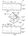
- FIG. 1 a cross-section of a pinch rectifier 100 in accordance with a first embodiment of my invention.
- Pinch rectifier 100 includes first and second semiconductor layers 102 and 104, preferably of silicon, which are doped to N conductivity type.
- Second layer 102 preferably comprises a bulk substrate that is highly doped to increase its conductivity.
- Second layer 104 preferably comprises a lightly doped layer expitaxially grown on substrate layer 102, the thickness and doping concentration of layer 104 determining the reverse breakdown voltage of rectifier 100 in a manner that will be apparent to those skilled in the art.
- Underlying substrate 102 is an electrode 106, such as aluminum, which constitutes the cathode of pinch rectifier 100 and which forms an ohmic contact with highly-doped layer 102.
- pinch rectifier 100 includes a plurality of semiconductor region portions 108 adjoining the upper portion of epitaxially layer 104 and being highly doped to P conductivity type.
- P region portions 108 constitute what are referred to herein as "current pinch-off means", the purpose of which will be described below in connection with Figures 3-5.
- Adjoining each of P region portions 108 is a further electrode 110, such as deposited aluminum, which constitutes the anode of pinch rectifier 100.
- P + region portions 108 have a dopant concentration per cubic centimeter preferably in excess of about 1 x 10 18 so that anode 110 forms an ohmic contact with P + region portions 108.
- Pinch rectifier 100 further includes third semiconductor layer portions 112 sandwiched between anode 110 and epitaxial layer 104 and which are highly doped to N conductivity type so that anode 110 forms an ohmic contact with epitaxial layer 104.
- N + region portions 112 comprise a plurality of individual regions arranged in a hexagonal, closely spaced format, that is, with N + region portion 114, for example, being symmetrically surrounded by six other like portions.
- P region portions 108 accordingly comprise an interconnected region with symmetrically interposed N + region portions 112.
- Other geometries may be employed, however, for example, with N + region portions 112 comprising square or parallel, elongated regions.
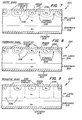
- Figure 3 illustrates the electrical condition of pinch rectifier 100 when such rectifier is biased with zero voltage, that is, with anode 110 electrically shorted to cathode 106.
- P + region portions 108 induce in epitaxial layer 104 depletion region portions 114 respectively extending into layer 104 from P region portions 108, which portions 114 arise from the inherent potential difference between the more highly doped P + portions 108 and the opposite conductivity type N - layer 104.
- Adjacent depletion region portions 114 merge together at a location indicated by an arrow 116, preferably at interface 118 between N + region portions 112 and epitaxial layer 104.
- N + region portions 112 to be of sufficiently small diameter, typically of 0.6 microns, at least with P + region portions doped to 1 x 1 0 18 per c.c. and N - epitaxial region 104 doped to 10 16 (per c.c.). It is not crucial that adjacent depletion region portions 114 merge at interface 118; however, if these depletion region portions 114 do not merge at interface 118, a higher than ideal reverse leakage current will result, and if adjacent depletion region portions 114 are merged at zero bias and also at low forward bias voltages (that is with anode 110 biased slightly nore positive than cathode 106), a higher than ideal forward voltage drop will result.
- Figure 4 illustrates the electrical condition of pinch rectifier 100 when forward biased.
- depletion region portions 114 are diminished from their size with pinch rectifier 100 under a zero biased condition, as illustrated in Figure 3.
- adjacent depletion region portions 114 do not merge but instead are spaced from each other so as to define conduction channel portions 120 in epitaxial layer 104 between adjacent depletion region portions 114. Since channel portions 120 are not depleted, they are able to conduct current through pinch rectifier 100.
- FIG 5 illustrates operation of pinch rectifier 100 when it is reversed biased, that is, with anode 110 biased with a negative voltage with respect to cathode 106. Under this reverse-biased condition, adjacent depletion region portions 114 are merged together, as at 122, so as to pinch-off conduction channel portions 120, which are shown in Figure 4. Accordingly, pinch rectifier 100 does not conduct current while in its reverse-biased condition, except for an extremely low level of reverse leakage current typically on the order of 10 microamperes, at least until pinch rectifier 100 is sufficiently reverse-biased to cause device breakdown (that is, uncontrolled current conduction due to avalanche breakdown).
- FIG. 6 there is illustrated a portion of a pinch rectifier 200 in accordance with a further embodiment of my invention.
- substrate layer 2C2, epitaxial layer 204, and cathode 206 suitably are essentially identical to substrate layer 102, epitaxial layer 104, and cathode layer 106, respectively, of pinch rectifier 100 ( Figure 1).
- pinch rectifier 200 the conductive material used to implement anode 230 is selected so as to form Schottky barrier contact portions 232 with epitaxial layer 204.
- a suitable material for anode 230 is, by way of example, aluminum or silicide which is highly-doped to either P or N conductivity type.
- the presense of Schottky barrier contact portions 232 results in the fabrication of P region portions 234 being easier than the fabrication of P + region portions 108 of pinch rectifier 100 ( Figure 1), as will become apparent from the following discussion of Figures 7-9, pertaining to the operation of pinch rectifier 200.
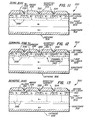
- Figure 7 illustrates operation of pinch rectifier 200 under a zero-biased condition.
- Extending into expitaxial layer 204 from current pinch-off region portions 234 are respective depletion region portions 236, which are shown as being spaced from each other.
- Conduction channel portions 238 exist between adjacent pairs of depletion region portions 236; however, these conduction channel portions 238 cannot conduct current through pinch rectifier 200 when it is slightly reverse biased, because Schottky barrier contact portions 232 block current flow for at least low levels of reverse voltages (as discussed further in conjunction with Figure 9).
- adjacent depletion region portions 236 there exists a tolerance in the spacing of adjacent depletion region portions 236 in the zero-biased condition of pinch rectifier 200. At one extreme, it would be permissible to have adjacent depletion region portions 236 merge, while at the other extreme, adjacent depletion region portions 236 may be spaced as far as possible from each other as long as Schottky barrier contact portions 232 prevent an undesirably high level of reverse leakage current when pinch rectifier 200 is reverse-biased to a degree in which adjacent depletion region portions 236 have not yet merged.
- Figure 8 illustrates operation of pinch rectifier 200 under a forward-biased condition.
- depletion region portions 236 are diminished in size from their size under a zero-biased condition (see Figure 7).
- the forward bias voltage on pinch rectifier 200 must exceed a threshold level for overcoming the potential barrier formed by Schottky barrier contact portions 232.
- the forward threshold voltage required for current conduction in current rectifier 200 be as low as possible.
- One suitable technique is the Shannon technique.
- As applied to pinch rectifier 200 a very thin, heavily-doped N conductivity type region (not shown) is provided between anode 230 and N epitaxial layer 204.
- a further suitable technique as applied to pinch rectifier 200 involves the creation of surface damage to N epitaxial layer 204, such as by reactive ion etching. The foregoing technioues are discussed in more detail in the following articles, respectively: J.M.
- FIG 9 the operation of pinch rectifier 200 in a sufficiently reverse-biased condition is illustrated. It can. be seen that adjacent depletion region portions 236 are merged together, resulting in pinch-off of conductive channel portions 238 that are shown in Figure 8. It is permissible for adjacent depletion region portions 236 not to be merged together at lower values of reverse bias, so long as Schottky barrier contact portions 232 then block current flow through pinch rectifier 200.
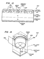
- FIG. 10 there is illustrated a pinch rectifier 300 in accordance with a further embodiment of my invention.
- substrate layer 302, epitaxial layer 304, and cathode 306 suitably are essentially identical to substrate layer 102, epitaxial layer 104, and cathode layer 106, respectively, of pinch rectifier 100 ( Figure 1).
- current pinch-off electrode portions 330 adjoin the upper portion of first epitaxial layer 304 and form Schottky barrier contact portions 331 therewith.
- a suitable material for implementing current pinch-off electrode portions 330 comprises aluminum or tungsten, by way of example.
Landscapes
- Electrodes Of Semiconductors (AREA)
Applications Claiming Priority (2)
| Application Number | Priority Date | Filing Date | Title |
|---|---|---|---|
| US06/510,520 US4641174A (en) | 1983-08-08 | 1983-08-08 | Pinch rectifier |
| US510520 | 1983-08-08 |
Publications (3)
| Publication Number | Publication Date |
|---|---|
| EP0134456A2 true EP0134456A2 (de) | 1985-03-20 |
| EP0134456A3 EP0134456A3 (en) | 1987-01-14 |
| EP0134456B1 EP0134456B1 (de) | 1991-07-17 |
Family
ID=24031095
Family Applications (1)
| Application Number | Title | Priority Date | Filing Date |
|---|---|---|---|
| EP84107496A Expired EP0134456B1 (de) | 1983-08-08 | 1984-06-28 | Pinch-Effekt-Gleichrichter |
Country Status (4)
| Country | Link |
|---|---|
| US (1) | US4641174A (de) |
| EP (1) | EP0134456B1 (de) |
| JP (1) | JPS6074582A (de) |
| DE (1) | DE3484811D1 (de) |
Cited By (5)
| Publication number | Priority date | Publication date | Assignee | Title |
|---|---|---|---|---|
| DE3631136A1 (de) * | 1986-09-12 | 1988-03-24 | Siemens Ag | Diode mit weichem abrissverhalten |
| DE4333618A1 (de) * | 1992-10-02 | 1994-04-07 | Fuji Electric Co Ltd | Schottky-Gleichrichter |
| EP0506450A3 (en) * | 1991-03-28 | 1994-08-24 | Murata Manufacturing Co | A schottky barrier diode and a method of manufacturing thereof |
| EP1850396A3 (de) * | 2006-04-28 | 2008-09-17 | Nissan Motor Co., Ltd. | Halbleiterbauelement und dessen Herstellungsmethode |
| RU2497263C2 (ru) * | 2007-11-30 | 2013-10-27 | Спал Аутомотиве С.Р.Л. | Вращающаяся электрическая машина и способ ее сборки |
Families Citing this family (73)
| Publication number | Priority date | Publication date | Assignee | Title |
|---|---|---|---|---|
| GB2137412B (en) * | 1983-03-15 | 1987-03-04 | Standard Telephones Cables Ltd | Semiconductor device |
| US4901120A (en) * | 1987-06-10 | 1990-02-13 | Unitrode Corporation | Structure for fast-recovery bipolar devices |
| US4827321A (en) * | 1987-10-29 | 1989-05-02 | General Electric Company | Metal oxide semiconductor gated turn off thyristor including a schottky contact |
| US4969027A (en) * | 1988-07-18 | 1990-11-06 | General Electric Company | Power bipolar transistor device with integral antisaturation diode |
| US4967243A (en) * | 1988-07-19 | 1990-10-30 | General Electric Company | Power transistor structure with high speed integral antiparallel Schottky diode |
| JP2667477B2 (ja) * | 1988-12-02 | 1997-10-27 | 株式会社東芝 | ショットキーバリアダイオード |
| US5111253A (en) * | 1989-05-09 | 1992-05-05 | General Electric Company | Multicellular FET having a Schottky diode merged therewith |
| US5814832A (en) * | 1989-09-07 | 1998-09-29 | Canon Kabushiki Kaisha | Electron emitting semiconductor device |
| JPH0750791B2 (ja) * | 1989-09-20 | 1995-05-31 | 株式会社日立製作所 | 半導体整流ダイオード及びそれを使つた電源装置並びに電子計算機 |
| US4994883A (en) * | 1989-10-02 | 1991-02-19 | General Electric Company | Field controlled diode (FCD) having MOS trench gates |
| US4982260A (en) * | 1989-10-02 | 1991-01-01 | General Electric Company | Power rectifier with trenches |
| JPH065736B2 (ja) * | 1989-12-15 | 1994-01-19 | 株式会社東芝 | ショットキー・ダイオード |
| US5345100A (en) * | 1991-03-29 | 1994-09-06 | Shindengen Electric Manufacturing Co., Ltd. | Semiconductor rectifier having high breakdown voltage and high speed operation |
| US5262669A (en) * | 1991-04-19 | 1993-11-16 | Shindengen Electric Manufacturing Co., Ltd. | Semiconductor rectifier having high breakdown voltage and high speed operation |
| JP2719295B2 (ja) * | 1993-04-09 | 1998-02-25 | リコー応用電子研究所株式会社 | 半導体整流装置 |
| US5365102A (en) * | 1993-07-06 | 1994-11-15 | North Carolina State University | Schottky barrier rectifier with MOS trench |
| US5612567A (en) * | 1996-05-13 | 1997-03-18 | North Carolina State University | Schottky barrier rectifiers and methods of forming same |
| US5859465A (en) * | 1996-10-15 | 1999-01-12 | International Rectifier Corporation | High voltage power schottky with aluminum barrier metal spaced from first diffused ring |
| JP3742204B2 (ja) * | 1996-11-21 | 2006-02-01 | 日世株式会社 | 成形焼き菓子の製造方法 |
| DE19723176C1 (de) * | 1997-06-03 | 1998-08-27 | Daimler Benz Ag | Leistungshalbleiter-Bauelement und Verfahren zu dessen Herstellung |
| US6362495B1 (en) | 1998-03-05 | 2002-03-26 | Purdue Research Foundation | Dual-metal-trench silicon carbide Schottky pinch rectifier |
| DE19819590C1 (de) * | 1998-04-30 | 1999-06-24 | Siemens Ag | MOS-Leistungstransistor |
| US6977420B2 (en) * | 1998-09-30 | 2005-12-20 | National Semiconductor Corporation | ESD protection circuit utilizing floating lateral clamp diodes |
| EP1222694B1 (de) * | 1999-09-22 | 2005-02-02 | SiCED Electronics Development GmbH & Co KG | SiC-Halbleitervorrichtung mit einem Schottky-Kontakt und Verfahren zu deren Herstellung |
| JP2001168351A (ja) | 1999-12-13 | 2001-06-22 | Fuji Electric Co Ltd | 半導体装置 |
| US6462393B2 (en) | 2001-03-20 | 2002-10-08 | Fabtech, Inc. | Schottky device |
| DE10259373B4 (de) * | 2002-12-18 | 2012-03-22 | Infineon Technologies Ag | Überstromfeste Schottkydiode mit niedrigem Sperrstrom |
| US20040188703A1 (en) * | 2003-03-07 | 2004-09-30 | Tongwei Cheng | Switch |
| DE10326739B3 (de) * | 2003-06-13 | 2005-03-24 | Infineon Technologies Ag | Halbleiterbauelement mit Schottky-Metallkontakt |
| DE10337457B3 (de) * | 2003-08-14 | 2005-01-20 | Infineon Technologies Ag | Transistorbauelement mit verbessertem Rückstromverhalten |
| US7262467B2 (en) * | 2003-09-10 | 2007-08-28 | Ixys Corporation | Over charge protection device |
| JP4623259B2 (ja) * | 2003-12-05 | 2011-02-02 | サンケン電気株式会社 | ショットキバリアを有する半導体装置 |
| JP4610207B2 (ja) * | 2004-02-24 | 2011-01-12 | 三洋電機株式会社 | 半導体装置およびその製造方法 |
| US7244970B2 (en) * | 2004-12-22 | 2007-07-17 | Tyco Electronics Corporation | Low capacitance two-terminal barrier controlled TVS diodes |
| JP2006295062A (ja) * | 2005-04-14 | 2006-10-26 | Rohm Co Ltd | 半導体装置 |
| US8901699B2 (en) | 2005-05-11 | 2014-12-02 | Cree, Inc. | Silicon carbide junction barrier Schottky diodes with suppressed minority carrier injection |
| JP2007281231A (ja) * | 2006-04-07 | 2007-10-25 | Shindengen Electric Mfg Co Ltd | 半導体装置 |
| JP5272323B2 (ja) * | 2006-04-28 | 2013-08-28 | 日産自動車株式会社 | 半導体装置とその製造方法 |
| US9437729B2 (en) | 2007-01-08 | 2016-09-06 | Vishay-Siliconix | High-density power MOSFET with planarized metalization |
| US9947770B2 (en) | 2007-04-03 | 2018-04-17 | Vishay-Siliconix | Self-aligned trench MOSFET and method of manufacture |
| US8368166B2 (en) * | 2007-05-30 | 2013-02-05 | Intersil Americas Inc. | Junction barrier Schottky diode |
| US7750426B2 (en) | 2007-05-30 | 2010-07-06 | Intersil Americas, Inc. | Junction barrier Schottky diode with dual silicides |
| TW200847448A (en) * | 2007-05-30 | 2008-12-01 | Intersil Inc | Junction barrier schottky diode |
| JP4333782B2 (ja) * | 2007-07-05 | 2009-09-16 | 株式会社デンソー | ジャンクションバリアショットキーダイオードを備えた炭化珪素半導体装置 |
| US9484451B2 (en) | 2007-10-05 | 2016-11-01 | Vishay-Siliconix | MOSFET active area and edge termination area charge balance |
| US7714365B2 (en) * | 2008-02-21 | 2010-05-11 | Infineon Technologies Austria Ag | Semiconductor component with Schottky zones in a drift zone |
| US20090224354A1 (en) * | 2008-03-05 | 2009-09-10 | Cree, Inc. | Junction barrier schottky diode with submicron channels |
| US8232558B2 (en) | 2008-05-21 | 2012-07-31 | Cree, Inc. | Junction barrier Schottky diodes with current surge capability |
| US8304829B2 (en) | 2008-12-08 | 2012-11-06 | Fairchild Semiconductor Corporation | Trench-based power semiconductor devices with increased breakdown voltage characteristics |
| US8174067B2 (en) * | 2008-12-08 | 2012-05-08 | Fairchild Semiconductor Corporation | Trench-based power semiconductor devices with increased breakdown voltage characteristics |
| US8227855B2 (en) * | 2009-02-09 | 2012-07-24 | Fairchild Semiconductor Corporation | Semiconductor devices with stable and controlled avalanche characteristics and methods of fabricating the same |
| US8148749B2 (en) * | 2009-02-19 | 2012-04-03 | Fairchild Semiconductor Corporation | Trench-shielded semiconductor device |
| US8049276B2 (en) * | 2009-06-12 | 2011-11-01 | Fairchild Semiconductor Corporation | Reduced process sensitivity of electrode-semiconductor rectifiers |
| US9443974B2 (en) | 2009-08-27 | 2016-09-13 | Vishay-Siliconix | Super junction trench power MOSFET device fabrication |
| DE102009047808B4 (de) * | 2009-09-30 | 2018-01-25 | Infineon Technologies Austria Ag | Bipolares Halbleiterbauelement und Verfahren zur Herstellung einer Halbleiterdiode |
| US9431530B2 (en) | 2009-10-20 | 2016-08-30 | Vishay-Siliconix | Super-high density trench MOSFET |
| US9117739B2 (en) * | 2010-03-08 | 2015-08-25 | Cree, Inc. | Semiconductor devices with heterojunction barrier regions and methods of fabricating same |
| JP5557581B2 (ja) * | 2010-04-08 | 2014-07-23 | 株式会社日立製作所 | 半導体装置および電力変換装置 |
| US8432000B2 (en) | 2010-06-18 | 2013-04-30 | Fairchild Semiconductor Corporation | Trench MOS barrier schottky rectifier with a planar surface using CMP techniques |
| US8680587B2 (en) | 2011-09-11 | 2014-03-25 | Cree, Inc. | Schottky diode |
| US8618582B2 (en) | 2011-09-11 | 2013-12-31 | Cree, Inc. | Edge termination structure employing recesses for edge termination elements |
| US8664665B2 (en) | 2011-09-11 | 2014-03-04 | Cree, Inc. | Schottky diode employing recesses for elements of junction barrier array |
| US20140048901A1 (en) * | 2011-09-26 | 2014-02-20 | Mitsubishi Electric Cororation | Rectifier of alternating-current generator for vehicle |
| CN103094356B (zh) * | 2011-11-04 | 2015-08-19 | 上海华虹宏力半导体制造有限公司 | 功率二极管的器件结构 |
| US9842911B2 (en) | 2012-05-30 | 2017-12-12 | Vishay-Siliconix | Adaptive charge balanced edge termination |
| US9722041B2 (en) | 2012-09-19 | 2017-08-01 | Vishay-Siliconix | Breakdown voltage blocking device |
| JP2014207460A (ja) * | 2014-05-28 | 2014-10-30 | 株式会社日立製作所 | 半導体装置および電力変換装置 |
| US9887259B2 (en) | 2014-06-23 | 2018-02-06 | Vishay-Siliconix | Modulated super junction power MOSFET devices |
| EP3183753B1 (de) | 2014-08-19 | 2025-03-19 | Vishay-Siliconix | Mosfet-halbleiteranordnung |
| KR102098996B1 (ko) | 2014-08-19 | 2020-04-08 | 비쉐이-실리코닉스 | 초접합 금속 산화물 반도체 전계 효과 트랜지스터 |
| CN106158982B (zh) * | 2015-04-08 | 2019-02-05 | 瀚薪科技股份有限公司 | 碳化硅接面能障萧特基整流器 |
| JP7468432B2 (ja) * | 2021-03-30 | 2024-04-16 | トヨタ自動車株式会社 | 半導体装置 |
| JP2022159760A (ja) * | 2021-04-05 | 2022-10-18 | ローム株式会社 | 半導体装置 |
Family Cites Families (17)
| Publication number | Priority date | Publication date | Assignee | Title |
|---|---|---|---|---|
| FR1317256A (fr) * | 1961-12-16 | 1963-02-08 | Teszner Stanislas | Perfectionnements aux dispositifs semi-conducteurs dits tecnetrons multibâtonnets |
| GB1208266A (en) * | 1966-12-09 | 1970-10-14 | Plessey Co Ltd | Improvements in or relating to integrated circuits |
| US3588671A (en) * | 1969-01-24 | 1971-06-28 | Nasa | Precision rectifier with fet switching means |
| JPS5217720B1 (de) * | 1971-07-31 | 1977-05-17 | ||
| JPS5329075B2 (de) * | 1972-02-12 | 1978-08-18 | ||
| US3982264A (en) * | 1973-04-25 | 1976-09-21 | Sony Corporation | Junction gated field effect transistor |
| US3953879A (en) * | 1974-07-12 | 1976-04-27 | Massachusetts Institute Of Technology | Current-limiting field effect device |
| JPS5935183B2 (ja) * | 1975-08-20 | 1984-08-27 | サンケイ電気 (株) | シヨツトキバリア半導体装置 |
| US4037245A (en) * | 1975-11-28 | 1977-07-19 | General Electric Company | Electric field controlled diode with a current controlling surface grid |
| GB1558506A (en) * | 1976-08-09 | 1980-01-03 | Mullard Ltd | Semiconductor devices having a rectifying metalto-semicondductor junction |
| JPS5846874B2 (ja) * | 1977-04-27 | 1983-10-19 | 三菱電機株式会社 | 接合型電界効果トランジスタ |
| US4170019A (en) * | 1977-08-05 | 1979-10-02 | General Electric Company | Semiconductor device with variable grid openings for controlling turn-off pattern |
| JPS54118781A (en) * | 1978-03-08 | 1979-09-14 | Mitsubishi Electric Corp | Planar-type diode |
| JPS5637683A (en) * | 1979-09-04 | 1981-04-11 | Nippon Telegr & Teleph Corp <Ntt> | Semiconductor rectifying device |
| JPS562672A (en) * | 1979-06-20 | 1981-01-12 | Shindengen Electric Mfg Co Ltd | Schottky barrier diode |
| US4236166A (en) * | 1979-07-05 | 1980-11-25 | Bell Telephone Laboratories, Incorporated | Vertical field effect transistor |
| JPS5635473A (en) * | 1979-08-29 | 1981-04-08 | Nippon Telegr & Teleph Corp <Ntt> | P-n junction type rectifying diode |
-
1983
- 1983-08-08 US US06/510,520 patent/US4641174A/en not_active Expired - Lifetime
-
1984
- 1984-06-28 EP EP84107496A patent/EP0134456B1/de not_active Expired
- 1984-06-28 DE DE8484107496T patent/DE3484811D1/de not_active Expired - Lifetime
- 1984-08-03 JP JP59163010A patent/JPS6074582A/ja active Granted
Cited By (8)
| Publication number | Priority date | Publication date | Assignee | Title |
|---|---|---|---|---|
| DE3631136A1 (de) * | 1986-09-12 | 1988-03-24 | Siemens Ag | Diode mit weichem abrissverhalten |
| EP0506450A3 (en) * | 1991-03-28 | 1994-08-24 | Murata Manufacturing Co | A schottky barrier diode and a method of manufacturing thereof |
| DE4333618A1 (de) * | 1992-10-02 | 1994-04-07 | Fuji Electric Co Ltd | Schottky-Gleichrichter |
| US5430323A (en) * | 1992-10-02 | 1995-07-04 | Fuji Electric Co., Ltd. | Injection control-type Schottky barrier rectifier |
| DE4333618C2 (de) * | 1992-10-02 | 1999-05-20 | Fuji Electric Co Ltd | Injektions-gesteuerter Schottky-Gleichrichter |
| EP1850396A3 (de) * | 2006-04-28 | 2008-09-17 | Nissan Motor Co., Ltd. | Halbleiterbauelement und dessen Herstellungsmethode |
| US7781802B2 (en) | 2006-04-28 | 2010-08-24 | Nissan Motor Co., Ltd. | Semiconductor device and manufacturing method thereof |
| RU2497263C2 (ru) * | 2007-11-30 | 2013-10-27 | Спал Аутомотиве С.Р.Л. | Вращающаяся электрическая машина и способ ее сборки |
Also Published As
| Publication number | Publication date |
|---|---|
| US4641174A (en) | 1987-02-03 |
| JPS6074582A (ja) | 1985-04-26 |
| EP0134456B1 (de) | 1991-07-17 |
| EP0134456A3 (en) | 1987-01-14 |
| DE3484811D1 (de) | 1991-08-22 |
| JPH0370907B2 (de) | 1991-11-11 |
Similar Documents
| Publication | Publication Date | Title |
|---|---|---|
| US4641174A (en) | Pinch rectifier | |
| US4982260A (en) | Power rectifier with trenches | |
| EP0122598B2 (de) | Hochgeschwindigkeitsdiode | |
| US4967243A (en) | Power transistor structure with high speed integral antiparallel Schottky diode | |
| US6184545B1 (en) | Semiconductor component with metal-semiconductor junction with low reverse current | |
| CA1085060A (en) | Semiconductor devices having a rectifying metal-to- semiconductor junction | |
| US5241195A (en) | Merged P-I-N/Schottky power rectifier having extended P-I-N junction | |
| CN100385676C (zh) | 碳化硅水平沟道缓冲栅极半导体器件 | |
| KR920010677B1 (ko) | 반도체장치 | |
| US4060821A (en) | Field controlled thyristor with buried grid | |
| KR100430834B1 (ko) | 쇼트키장벽정류기와그제조방법 | |
| CA1131801A (en) | Semiconductor device | |
| US4969028A (en) | Gate enhanced rectifier | |
| US5859465A (en) | High voltage power schottky with aluminum barrier metal spaced from first diffused ring | |
| US20010013613A1 (en) | Semiconductor device and a method of fabricating material for a semiconductor device | |
| JP7582733B2 (ja) | 炭化珪素からなるトレンチゲート構造の縦型mosfet | |
| KR100514398B1 (ko) | 실리콘 카바이드 전계제어 바이폴라 스위치 | |
| US5345100A (en) | Semiconductor rectifier having high breakdown voltage and high speed operation | |
| TWI776173B (zh) | 碳化矽半導體元件 | |
| US4047196A (en) | High voltage semiconductor device having a novel edge contour | |
| JP2020088054A (ja) | パワー半導体装置 | |
| US4933740A (en) | Insulated gate transistor with vertical integral diode and method of fabrication | |
| EP0116651A1 (de) | Photothyristor | |
| US6753588B2 (en) | Semiconductor rectifier | |
| EP0064614A2 (de) | Emitterstruktur für Halbleiteranordnungen |
Legal Events
| Date | Code | Title | Description |
|---|---|---|---|
| PUAI | Public reference made under article 153(3) epc to a published international application that has entered the european phase |
Free format text: ORIGINAL CODE: 0009012 |
|
| AK | Designated contracting states |
Designated state(s): DE FR NL |
|
| PUAL | Search report despatched |
Free format text: ORIGINAL CODE: 0009013 |
|
| AK | Designated contracting states |
Kind code of ref document: A3 Designated state(s): DE FR NL |
|
| 17P | Request for examination filed |
Effective date: 19870602 |
|
| 17Q | First examination report despatched |
Effective date: 19881019 |
|
| GRAA | (expected) grant |
Free format text: ORIGINAL CODE: 0009210 |
|
| AK | Designated contracting states |
Kind code of ref document: B1 Designated state(s): DE FR NL |
|
| ET | Fr: translation filed | ||
| REF | Corresponds to: |
Ref document number: 3484811 Country of ref document: DE Date of ref document: 19910822 |
|
| PLBE | No opposition filed within time limit |
Free format text: ORIGINAL CODE: 0009261 |
|
| STAA | Information on the status of an ep patent application or granted ep patent |
Free format text: STATUS: NO OPPOSITION FILED WITHIN TIME LIMIT |
|
| 26N | No opposition filed | ||
| PGFP | Annual fee paid to national office [announced via postgrant information from national office to epo] |
Ref country code: NL Payment date: 20010611 Year of fee payment: 18 |
|
| PGFP | Annual fee paid to national office [announced via postgrant information from national office to epo] |
Ref country code: FR Payment date: 20020530 Year of fee payment: 19 |
|
| PGFP | Annual fee paid to national office [announced via postgrant information from national office to epo] |
Ref country code: DE Payment date: 20020620 Year of fee payment: 19 |
|
| PG25 | Lapsed in a contracting state [announced via postgrant information from national office to epo] |
Ref country code: NL Free format text: LAPSE BECAUSE OF NON-PAYMENT OF DUE FEES Effective date: 20030101 |
|
| NLV4 | Nl: lapsed or anulled due to non-payment of the annual fee |
Effective date: 20030101 |
|
| PG25 | Lapsed in a contracting state [announced via postgrant information from national office to epo] |
Ref country code: DE Free format text: LAPSE BECAUSE OF NON-PAYMENT OF DUE FEES Effective date: 20040101 |
|
| PG25 | Lapsed in a contracting state [announced via postgrant information from national office to epo] |
Ref country code: FR Free format text: LAPSE BECAUSE OF NON-PAYMENT OF DUE FEES Effective date: 20040227 |
|
| REG | Reference to a national code |
Ref country code: FR Ref legal event code: ST |