EP0122598B2 - Hochgeschwindigkeitsdiode - Google Patents
Hochgeschwindigkeitsdiode Download PDFInfo
- Publication number
- EP0122598B2 EP0122598B2 EP84104089A EP84104089A EP0122598B2 EP 0122598 B2 EP0122598 B2 EP 0122598B2 EP 84104089 A EP84104089 A EP 84104089A EP 84104089 A EP84104089 A EP 84104089A EP 0122598 B2 EP0122598 B2 EP 0122598B2
- Authority
- EP
- European Patent Office
- Prior art keywords
- layer
- electrode
- speed diode
- thickness
- impurity concentration
- Prior art date
- Legal status (The legal status is an assumption and is not a legal conclusion. Google has not performed a legal analysis and makes no representation as to the accuracy of the status listed.)
- Expired
Links
Images

Classifications
-
- H—ELECTRICITY
- H10—SEMICONDUCTOR DEVICES; ELECTRIC SOLID-STATE DEVICES NOT OTHERWISE PROVIDED FOR
- H10D—INORGANIC ELECTRIC SEMICONDUCTOR DEVICES
- H10D8/00—Diodes
-
- H—ELECTRICITY
- H10—SEMICONDUCTOR DEVICES; ELECTRIC SOLID-STATE DEVICES NOT OTHERWISE PROVIDED FOR
- H10D—INORGANIC ELECTRIC SEMICONDUCTOR DEVICES
- H10D62/00—Semiconductor bodies, or regions thereof, of devices having potential barriers
- H10D62/80—Semiconductor bodies, or regions thereof, of devices having potential barriers characterised by the materials
- H10D62/83—Semiconductor bodies, or regions thereof, of devices having potential barriers characterised by the materials being Group IV materials, e.g. B-doped Si or undoped Ge
- H10D62/834—Semiconductor bodies, or regions thereof, of devices having potential barriers characterised by the materials being Group IV materials, e.g. B-doped Si or undoped Ge further characterised by the dopants
Definitions
- the present invention relates to a diode which has a PNN + structure and can operate at high speed.
- the switching frequency of the regulator has been increased to 50 KHz or more, and a switching regulator having a frequency of 200 to 300 KHz will be put to practical use in the near future.
- the switching regulator of this kind is required to include a high-speed diode which is short in reverse recovery time (trr) and small in forward voltage drop V F .
- trr reverse recovery time
- V F forward voltage drop
- High-speed diodes which are suitable for use in a switching regulator and now are commercially available, are classified roughly in two groups from the structural point of view.
- One of the groups is a Schottky barrier diode for a low voltage source such as a 5-volt power source.
- the Schottky barrier diode is advantageous in that the reverse recovery time (trr) is tens of nanoseconds or less since no minority carriers are stored, and in that the forward voltage drop V F can be reduced to a value of 0.5 to 0.6 V by appropriately selecting the height of the Schottky barrier.
- this diode has a drawback that the breakdown voltage V R is low, that is, lies in a range from 40 to 50 V.
- the other group is a high-speed diode with a PNN* (PvN, PnN or PIN) structure for relatively high voltage sources such as a 12-volt power source and a 24-volt power source.
- This diode has a reduced capacitance and a breakdown voltage of 100 to 200 V due to the existence of a high resistivity region between the cathode and anode, but is found to have the following drawbacks.
- the forward voltage drop V F is relatively high, that is, about 1 V
- the reverse recovery time (trr) is hundreds of nanoseconds since minority carriers are stored. Further, the present inventors have found that the reverse recovery current rises abruptly, and considerable noise is produced in the packaged diode.
- a diode comprising a PNN + structure and two electrodes which make ohmic contact to the device.
- the P region is highly doped close to the rectifying junction, the N layer is as thin and its resistivity as low as possible with respect to the breakdown voltage requirements and a carrier lifetime reducing agent is introduced throughout the semiconductor pellet.
- An object of the present invention is to provide a high-speed diode which shows a high breakdown voltage, a small forward voltage drop, and a low noise level in the packaged device.
- Another object of the present invention is to provide a high-speed diode which has a breakdown voltage of about 200 V, a forward voltage drop of 0.9 V or less, a reverse recovery time of 50 nsec or less, and a soft reverse recovery characteristic.
- Fig. 1a shows, in section, an embodiment of a high-speed diode according to the present invention.
- an N+ -silicon substrate 1 is used which is doped with antimony so as to have a low resistivity of 0.015 0 cm.
- An N-layer 2 having a resistivity of 5 to 12 0 cm is grown epitaxially on the substrate 1 to a thickness of 27 pm.
- the whole surface of the silicon wafer thus formed is oxidized to form an Si0 2 film 5.
- the Si0 2 film on the bottom side of the silicon substrate 1 is removed, and an N ++ -silicon layer 3 is formed at the bottom surface of the substrate 1, to realize a low resistance ohmic contact with an electrode.
- the N ++ -layer 3 has the conductivity of N-type, and a higher impurity concentration than the N +- silicon substrate 1. Then, the Si0 2 film 5 on the N-layer 2 is selectively removed by the well-known photolithography to provide apertures in the Si0 2 film 5, and boron is diffused into the N-layer 2 through the apertures to form a P-layer 4 having a depth of 5 ⁇ m. Accordingly, the P-layer 4 is surrounded by the N-layer 2 in the surface thereof, and a planar structure is formed.
- the silicon wafer thus treated is doped with a heavy metal capable of acting as a lifetime killer (for example, gold or platinum) so that the carrier lifetime is equal to 22 nsec.
- a lifetime killer for example, gold or platinum
- a field plate electrode 6 and a contact electrode 7 are formed, through evaporation techniques, on the upper and lower surfaces of the silicon wafer, respectively. Finally, the wafer thus produced is separated into individual diode pellets to obtain the devices shown in Fig. 1a.
- Fig. 1b shows the variation of impurity concentration with depth in the silicon pellet shown in Fig. 1a. That is, the distance from the surface of the silicon pellet is plotted as abscissa, and the impurity concentration as ordinate. In Fig. 1b, numerical values written alongside the abscissa indicate the thickness of the silicon layers 1 to 4 in micrometers.
- the field plate electrode 6 is made of aluminum or has a multi-layer structure such as Aa-Cr-Ni-Ag, Cr-Ni-Ag, or Ti-Ni-Ag, and the contact electrode 7 has a multi-layer structure such as Cr-Ni-Ag or Ti-Ni-Ag.
- the field plate electrode 6 is extended on the Si0 2 film 5 so as to go beyond that end of a PN junction formed between the layers 2 and 4 which is exposed at the surface of the semiconductor pellet, in order to prevent a reduction in breakdown voltage due to the variation of the surface charge of the Si0 2 film 5 with time.
- Fig. 2 shows the current waveform at a time a high-speed diode is put from a forward conductive state into a reverse blocking state.
- the current characteristic of a high-speed diode can be expressed by a reverse recovery time (trr), a peak reverse current l rp , and the time derivative of a reverse recovery current d lr ,/dt at the risetime thereof.
- the high-speed diode In order to reduce a switching loss, it is required to make short the reverse recovery time (trr) and to make small the peak reverse current l rp , Further, in order to decrease noise ascribed to a switching regulator, it is required to make small both of I r p and dl r /dt, that is, the high-speed diode is required to have a soft recovery characteristic. In other words, it is desirable that the high-speed diode used in a switching regulator is small in each of three parameters, trr, l r p, and dl r /dt. Specifically, when the parameter dl r /dt is made small to obtain a soft recovery characteristic, noise in the switching regulator is reduced. Accordingly, a snubber circuit coupled with the switching regulator can be made small in size, and thus a power unit can be miniaturized.
- the N-layer 2 has an impurity concentration of 2 ⁇ 10 15 atoms/cm 3 or less, that is, a resistivity of 2.5 ⁇ cm or more. Accordingly, the resistivity of the N-layer 2 is put in a range from 5 to 12 ⁇ ! cm, to grow the N-layer 2 without difficulty. Incidentally, even an N-layer having a resistivity of about 100 ⁇ cm can be used.
- the forward voltage drop V F depends upon the lifetime T of carriers and the thickness t N of the N-layer 2.
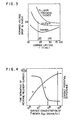
- the forward voltage drop V F was found to increase greatly as the carrier lifetime T is smaller, as shown in Fig. 3. Accordingly, it is undesirable to make the thickness t N of the N-layer 2 greater than 25 pm.
- the forward voltage drop V F decreased with decreasing carrier lifetime, till the forward voltage drop V F reaches a minimum value, and then increases with decreasing carrier lifetime. Accordingly, it is desirable to make the thickness t N smaller than 25 pm. While, in order to obtain a breakdown voltage of about 200 V, a depletion layer with a desired width has to be formed. That is, it is impossible to make the thickness t N extremely small. Accordingly, the lower limit of the thickness t N is 19 pm.
- the carrier lifetime T in the N-layer 2 is required to be equal to or less than 40 nsec, taking into consideration actual circuit conditions given to the embodiment.
- the forward voltage drop V F increases abruptly when the carrier lifetime T becomes smaller than 20 nsec. Accordingly, a lower limit of the carrier lifetime T is 20 nsec.
- the thickness of the P-layer 4 namely, the depth x j of the PN junction is equal to or less than 6 ⁇ m.
- the depth x j has to be made equal to or greater than 2 ⁇ m.
- Fig. 4 shows a relation between the surface impurity concentration N s p of the P-layer 4 and the parameter dl/dt, which is obtained under the above-explained restrictions on the resistivity and thickness of the N-layer 2, the carrier lifetime in the N-layer 2, and the thickness of the P-layer 4.
- the time derivative of reverse recovery current dl/dt decreases as the surface impurity concentration N s p is smaller, and a favorable, soft recovery characteristic is obtained when the surface impurity concentration N sp is equal to or less than 8 x 10 18 atomslcm 3 .
- the contact potential difference between the electrode 6 and P-layer 4 increases greatly when the surface impurity concentration N sp is made small, as shown in Fig. 4. Accordingly, the surface impurity concentration N sp cannot be made smaller than a value, which depends upon the material for forming the electrode 6.
- the present inventor's investigation it has been found that, in the case where the electrode 6 is made of an ordinary electrode material, the above-mentioned contact potential difference has a desired value when the surface impurity concentration N sp is made equal to or greater than 8 x 10¹⁷ atoms/cm 3 .
- the embodiment shown in Figs. 1a and 1b which satisfies the above-mentioned requirements with respect to the resistivity and thickness of the N-layer 2, the carrier lifetime in the N-layer 2, the thickness of the P-layer 4, and the surface impurity concentration of the P-layer 4, has a breakdown voltage V R of 200 V, a forward voltage drop V F of 0.9 V or less, a reverse recovery time (trr) of 50 nsec or less, and a soft recovery characteristic. Accordingly, a switching regulator including the present embodiment can operate at a high frequency. Further, even when a considerable time has elapsed, the breakdown voltage V R of the present embodiment is prevented from decreasing, by the action of the field plate electrode 6.
- the Si0 2 film 5 may be replaced by one of various insulating films capable of serving as a passivation film such as an Si 3 N 4 film, an Si0 2 -B 2 0 3 -ZnO glass film, and a PbO-SiO 2 -B 2 0 3 glass film.
- the contact electrode 7 may be put in ohmic contact with the N + -layer 1 without any intervening layer between the electrode 7 and the N +- layer 1.
Landscapes
- Electrodes Of Semiconductors (AREA)
Claims (6)
Applications Claiming Priority (2)
| Application Number | Priority Date | Filing Date | Title |
|---|---|---|---|
| JP58066152A JPS59189679A (ja) | 1983-04-13 | 1983-04-13 | ダイオ−ド |
| JP66152/83 | 1983-04-13 |
Publications (4)
| Publication Number | Publication Date |
|---|---|
| EP0122598A2 EP0122598A2 (de) | 1984-10-24 |
| EP0122598A3 EP0122598A3 (en) | 1985-09-18 |
| EP0122598B1 EP0122598B1 (de) | 1987-03-11 |
| EP0122598B2 true EP0122598B2 (de) | 1990-04-04 |
Family
ID=13307603
Family Applications (1)
| Application Number | Title | Priority Date | Filing Date |
|---|---|---|---|
| EP84104089A Expired EP0122598B2 (de) | 1983-04-13 | 1984-04-11 | Hochgeschwindigkeitsdiode |
Country Status (4)
| Country | Link |
|---|---|
| US (1) | US4594602A (de) |
| EP (1) | EP0122598B2 (de) |
| JP (1) | JPS59189679A (de) |
| DE (1) | DE3462642D1 (de) |
Families Citing this family (35)
| Publication number | Priority date | Publication date | Assignee | Title |
|---|---|---|---|---|
| FR2581252B1 (fr) * | 1985-04-26 | 1988-06-10 | Radiotechnique Compelec | Composant semiconducteur du type planar a structure d'anneaux de garde, famille de tels composants et procede de realisation |
| JPS62115880A (ja) * | 1985-11-15 | 1987-05-27 | Shindengen Electric Mfg Co Ltd | Pn接合素子 |
| US4775643A (en) * | 1987-06-01 | 1988-10-04 | Motorola Inc. | Mesa zener diode and method of manufacture thereof |
| JPH0642542B2 (ja) * | 1988-04-08 | 1994-06-01 | 株式会社東芝 | 高耐圧半導体装置の製造方法 |
| DE3823795A1 (de) * | 1988-07-14 | 1990-01-18 | Semikron Elektronik Gmbh | Schnelle leistungsdiode |
| US5017950A (en) * | 1989-01-19 | 1991-05-21 | Toko, Inc. | Variable-capacitance diode element having wide capacitance variation range |
| JP3074736B2 (ja) * | 1990-12-28 | 2000-08-07 | 富士電機株式会社 | 半導体装置 |
| DE4135259C1 (de) * | 1991-10-25 | 1993-01-07 | Semikron Elektronik Gmbh, 8500 Nuernberg, De | |
| JPH06314801A (ja) * | 1993-03-05 | 1994-11-08 | Mitsubishi Electric Corp | 半導体装置およびその製造方法 |
| JPH08125200A (ja) * | 1994-10-25 | 1996-05-17 | Mitsubishi Electric Corp | 半導体装置及びその製造方法 |
| JP3994443B2 (ja) * | 1995-05-18 | 2007-10-17 | 三菱電機株式会社 | ダイオード及びその製造方法 |
| JPH07326772A (ja) * | 1995-05-25 | 1995-12-12 | Rohm Co Ltd | 個別ダイオード装置 |
| JPH0818071A (ja) * | 1995-05-25 | 1996-01-19 | Rohm Co Ltd | 個別ダイオード装置の製造方法 |
| JPH088446A (ja) * | 1995-05-25 | 1996-01-12 | Rohm Co Ltd | 個別ダイオード装置 |
| DE19536022A1 (de) * | 1995-09-27 | 1997-04-03 | Siemens Ag | Diode mit hoher Stoßstromfestigkeit und weichem Abschaltverhalten |
| JP3444081B2 (ja) * | 1996-02-28 | 2003-09-08 | 株式会社日立製作所 | ダイオード及び電力変換装置 |
| CN1057404C (zh) * | 1996-04-02 | 2000-10-11 | 电子科技大学 | 锗硅异质结低正向压降高速二极管 |
| US5859465A (en) * | 1996-10-15 | 1999-01-12 | International Rectifier Corporation | High voltage power schottky with aluminum barrier metal spaced from first diffused ring |
| DE19837944A1 (de) * | 1998-08-21 | 2000-02-24 | Asea Brown Boveri | Verfahren zur Fertigung eines Halbleiterbauelements |
| JP2003512725A (ja) * | 1999-10-20 | 2003-04-02 | コーニンクレッカ フィリップス エレクトロニクス エヌ ヴィ | 半導体装置、この半導体装置の製造方法およびこの半導体装置が設けられた回路 |
| US6632730B1 (en) | 1999-11-23 | 2003-10-14 | Ebara Solar, Inc. | Method for self-doping contacts to a semiconductor |
| JP4080659B2 (ja) * | 2000-01-28 | 2008-04-23 | 三菱電機株式会社 | 半導体装置 |
| US6737731B1 (en) | 2000-06-26 | 2004-05-18 | Fairchild Semiconductor Corporation | Soft recovery power diode |
| DE10031461B4 (de) * | 2000-06-28 | 2006-06-29 | Infineon Technologies Ag | Hochvolt-Diode |
| DE10126627A1 (de) * | 2001-05-31 | 2002-12-12 | Infineon Technologies Ag | Halbleiterstruktur und Verfahren zur Verbesserung der ESD-Festigkeit derselben |
| JP4000927B2 (ja) * | 2002-07-03 | 2007-10-31 | 富士電機デバイステクノロジー株式会社 | 半導体装置およびその製造方法 |
| US7189610B2 (en) * | 2004-10-18 | 2007-03-13 | Semiconductor Components Industries, L.L.C. | Semiconductor diode and method therefor |
| JP5078314B2 (ja) * | 2006-10-18 | 2012-11-21 | ローム株式会社 | ショットキーバリアダイオードおよびその製造方法 |
| CN102208454B (zh) * | 2010-03-31 | 2013-03-13 | 比亚迪股份有限公司 | 快速恢复二极管 |
| JP2012186353A (ja) * | 2011-03-07 | 2012-09-27 | Fuji Electric Co Ltd | 複合半導体装置 |
| DE112015000206T5 (de) * | 2014-10-03 | 2016-08-25 | Fuji Electric Co., Ltd. | Halbleitervorrichtung und Verfahren zum Herstellen einer Halbleitervorrichtung |
| DE102016117389B4 (de) * | 2015-11-20 | 2020-05-28 | Semikron Elektronik Gmbh & Co. Kg | Leistungshalbleiterchip und Verfahren zur Herstellung eines Leistungshalbleiterchips und Leistungshalbleitereinrichtung |
| JP6846119B2 (ja) * | 2016-05-02 | 2021-03-24 | 株式会社 日立パワーデバイス | ダイオード、およびそれを用いた電力変換装置 |
| CN107623045A (zh) * | 2017-09-30 | 2018-01-23 | 绍兴上虞欧菲光电科技有限公司 | 一种二极管 |
| CN109801978B (zh) * | 2019-03-13 | 2024-03-19 | 捷捷半导体有限公司 | 低压降二极管及其制备方法 |
Family Cites Families (11)
| Publication number | Priority date | Publication date | Assignee | Title |
|---|---|---|---|---|
| US3553536A (en) * | 1968-11-19 | 1971-01-05 | Rca Corp | Semiconductor rectifiers having controlled storage and recovery characteristics |
| US4180422A (en) * | 1969-02-03 | 1979-12-25 | Raytheon Company | Method of making semiconductor diodes |
| JPS4921984B1 (de) * | 1969-05-28 | 1974-06-05 | ||
| US3964084A (en) * | 1974-06-12 | 1976-06-15 | Bell Telephone Laboratories, Incorporated | Schottky barrier diode contacts |
| FR2287774A1 (fr) * | 1974-10-08 | 1976-05-07 | Antennes Moulees Plastiques | Nouvelle application de diodes pour la commutation de puissance en hyperfrequence |
| FR2288390A1 (fr) * | 1974-10-18 | 1976-05-14 | Thomson Csf | Procede de realisation d'une structure semi-conductrice pour hyperfrequence et composant electronique ainsi obtenu |
| DE2608432C3 (de) * | 1976-03-01 | 1981-07-09 | Siemens AG, 1000 Berlin und 8000 München | Leistungsdiode |
| JPS5645081A (en) * | 1979-09-19 | 1981-04-24 | Toshiba Corp | Low-loss diode |
| JPS5645082A (en) * | 1979-09-19 | 1981-04-24 | Toshiba Corp | Low-loss diode |
| JPS57132370A (en) * | 1981-02-09 | 1982-08-16 | Toshiba Corp | Low-loss diode |
| JPS5839070A (ja) * | 1981-08-31 | 1983-03-07 | Toshiba Corp | 半導体装置 |
-
1983
- 1983-04-13 JP JP58066152A patent/JPS59189679A/ja active Pending
-
1984
- 1984-04-11 EP EP84104089A patent/EP0122598B2/de not_active Expired
- 1984-04-11 US US06/599,166 patent/US4594602A/en not_active Expired - Fee Related
- 1984-04-11 DE DE8484104089T patent/DE3462642D1/de not_active Expired
Also Published As
| Publication number | Publication date |
|---|---|
| DE3462642D1 (en) | 1987-04-16 |
| US4594602A (en) | 1986-06-10 |
| EP0122598B1 (de) | 1987-03-11 |
| JPS59189679A (ja) | 1984-10-27 |
| EP0122598A3 (en) | 1985-09-18 |
| EP0122598A2 (de) | 1984-10-24 |
Similar Documents
| Publication | Publication Date | Title |
|---|---|---|
| EP0122598B1 (de) | Hochgeschwindigkeitsdiode | |
| US4641174A (en) | Pinch rectifier | |
| US6436779B2 (en) | Semiconductor device having a plurality of resistive paths | |
| EP0902981B1 (de) | Schottkybarriere gleichrichter | |
| EP0707744B1 (de) | Schottky-gleichrichter mit mos-gräben | |
| US6624472B2 (en) | Semiconductor device with voltage sustaining zone | |
| EP1947700B1 (de) | Niederspannungsdiode mit verringertem parasitären Widerstand und Verfahren zu ihrer Herstellung | |
| EP0526897A2 (de) | Tunneleffektanordnung mit drei Elektroden | |
| US6674152B2 (en) | Bipolar diode | |
| EP0074642B1 (de) | Schnelle, verlustarme Dioden | |
| EP0979531B1 (de) | Siliziumkarbid feldgesteuerter zweipoliger schalter | |
| US4476481A (en) | Low-loss P-i-n diode | |
| US5345100A (en) | Semiconductor rectifier having high breakdown voltage and high speed operation | |
| EP0160525B1 (de) | GTO-Thyristor und Verfahren zu dessen Herstellung | |
| US4849800A (en) | Semiconductor component | |
| GB1587540A (en) | Gate turn-off diodes and arrangements including such diodes | |
| US4146906A (en) | Low forward voltage drop semiconductor device having polycrystalline layers of different resistivity | |
| JP3072753B2 (ja) | 半導体装置及び製造方法 | |
| US4551744A (en) | High switching speed semiconductor device containing graded killer impurity | |
| EP1008187B1 (de) | Halbleiter mit gleichrichtendem übergang und seine herstellung | |
| EP0157207A2 (de) | Mittels Steuerelektrode abschaltbarer Thyristor | |
| EP0033496B1 (de) | Halbleitervorrichtung mit drei Anschlussklemmen | |
| RU2045111C1 (ru) | Полупроводниковый прибор | |
| JPH08316499A (ja) | 高速ダイオード | |
| KR940005455B1 (ko) | 실리콘 배리스터의 제조방법 |
Legal Events
| Date | Code | Title | Description |
|---|---|---|---|
| PUAI | Public reference made under article 153(3) epc to a published international application that has entered the european phase |
Free format text: ORIGINAL CODE: 0009012 |
|
| AK | Designated contracting states |
Designated state(s): CH DE FR GB IT LI NL SE |
|
| PUAL | Search report despatched |
Free format text: ORIGINAL CODE: 0009013 |
|
| AK | Designated contracting states |
Designated state(s): CH DE FR GB IT LI NL SE |
|
| 17P | Request for examination filed |
Effective date: 19850919 |
|
| 17Q | First examination report despatched |
Effective date: 19860515 |
|
| GRAA | (expected) grant |
Free format text: ORIGINAL CODE: 0009210 |
|
| AK | Designated contracting states |
Kind code of ref document: B1 Designated state(s): DE FR |
|
| REF | Corresponds to: |
Ref document number: 3462642 Country of ref document: DE Date of ref document: 19870416 |
|
| ET | Fr: translation filed | ||
| PLBI | Opposition filed |
Free format text: ORIGINAL CODE: 0009260 |
|
| 26 | Opposition filed |
Opponent name: TELEFUNKEN ELECTRONIC GMBH Effective date: 19871210 |
|
| PUAH | Patent maintained in amended form |
Free format text: ORIGINAL CODE: 0009272 |
|
| STAA | Information on the status of an ep patent application or granted ep patent |
Free format text: STATUS: PATENT MAINTAINED AS AMENDED |
|
| 27A | Patent maintained in amended form |
Effective date: 19900404 |
|
| AK | Designated contracting states |
Kind code of ref document: B2 Designated state(s): CH DE FR GB IT LI NL SE |
|
| ET3 | Fr: translation filed ** decision concerning opposition | ||
| PGFP | Annual fee paid to national office [announced via postgrant information from national office to epo] |
Ref country code: FR Payment date: 19970320 Year of fee payment: 14 |
|
| PGFP | Annual fee paid to national office [announced via postgrant information from national office to epo] |
Ref country code: DE Payment date: 19970630 Year of fee payment: 14 |
|
| PG25 | Lapsed in a contracting state [announced via postgrant information from national office to epo] |
Ref country code: FR Free format text: THE PATENT HAS BEEN ANNULLED BY A DECISION OF A NATIONAL AUTHORITY Effective date: 19980430 |
|
| PG25 | Lapsed in a contracting state [announced via postgrant information from national office to epo] |
Ref country code: DE Free format text: LAPSE BECAUSE OF NON-PAYMENT OF DUE FEES Effective date: 19990202 |
|
| REG | Reference to a national code |
Ref country code: FR Ref legal event code: ST |