EP0135190B1 - Régulateur à commutation muni d'un comparateur alimenté par une grandeur de comparaison périodique ayant un déroulement temporel donné - Google Patents
Régulateur à commutation muni d'un comparateur alimenté par une grandeur de comparaison périodique ayant un déroulement temporel donné Download PDFInfo
- Publication number
- EP0135190B1 EP0135190B1 EP84110881A EP84110881A EP0135190B1 EP 0135190 B1 EP0135190 B1 EP 0135190B1 EP 84110881 A EP84110881 A EP 84110881A EP 84110881 A EP84110881 A EP 84110881A EP 0135190 B1 EP0135190 B1 EP 0135190B1
- Authority
- EP
- European Patent Office
- Prior art keywords
- voltage
- switching regulator
- comparator
- output
- generator
- Prior art date
- Legal status (The legal status is an assumption and is not a legal conclusion. Google has not performed a legal analysis and makes no representation as to the accuracy of the status listed.)
- Expired
Links
- 230000000737 periodic effect Effects 0.000 title claims description 4
- 230000002123 temporal effect Effects 0.000 title 1
- 239000003990 capacitor Substances 0.000 claims description 18
- 230000001105 regulatory effect Effects 0.000 claims description 3
- 230000001419 dependent effect Effects 0.000 claims description 2
- 230000005679 Peltier effect Effects 0.000 claims 2
- 238000001816 cooling Methods 0.000 abstract description 5
- 230000007423 decrease Effects 0.000 abstract description 2
- 230000005669 field effect Effects 0.000 description 12
- 230000000903 blocking effect Effects 0.000 description 4
- 230000007704 transition Effects 0.000 description 4
- 230000005540 biological transmission Effects 0.000 description 2
- 238000000034 method Methods 0.000 description 2
- 238000011144 upstream manufacturing Methods 0.000 description 2
- 230000033228 biological regulation Effects 0.000 description 1
- 230000001276 controlling effect Effects 0.000 description 1
- 230000000694 effects Effects 0.000 description 1
- 238000005516 engineering process Methods 0.000 description 1
- 230000010354 integration Effects 0.000 description 1
- 238000011835 investigation Methods 0.000 description 1
- 239000013307 optical fiber Substances 0.000 description 1
- 230000035945 sensitivity Effects 0.000 description 1
Images
Classifications
-
- H—ELECTRICITY
- H02—GENERATION; CONVERSION OR DISTRIBUTION OF ELECTRIC POWER
- H02M—APPARATUS FOR CONVERSION BETWEEN AC AND AC, BETWEEN AC AND DC, OR BETWEEN DC AND DC, AND FOR USE WITH MAINS OR SIMILAR POWER SUPPLY SYSTEMS; CONVERSION OF DC OR AC INPUT POWER INTO SURGE OUTPUT POWER; CONTROL OR REGULATION THEREOF
- H02M3/00—Conversion of DC power input into DC power output
- H02M3/02—Conversion of DC power input into DC power output without intermediate conversion into AC
- H02M3/04—Conversion of DC power input into DC power output without intermediate conversion into AC by static converters
- H02M3/10—Conversion of DC power input into DC power output without intermediate conversion into AC by static converters using discharge tubes with control electrode or semiconductor devices with control electrode
- H02M3/145—Conversion of DC power input into DC power output without intermediate conversion into AC by static converters using discharge tubes with control electrode or semiconductor devices with control electrode using devices of a triode or transistor type requiring continuous application of a control signal
- H02M3/155—Conversion of DC power input into DC power output without intermediate conversion into AC by static converters using discharge tubes with control electrode or semiconductor devices with control electrode using devices of a triode or transistor type requiring continuous application of a control signal using semiconductor devices only
- H02M3/156—Conversion of DC power input into DC power output without intermediate conversion into AC by static converters using discharge tubes with control electrode or semiconductor devices with control electrode using devices of a triode or transistor type requiring continuous application of a control signal using semiconductor devices only with automatic control of output voltage or current, e.g. switching regulators
Definitions
- the invention relates to a switching regulator as specified in the preamble of claim 1 with a comparator, to which a periodic comparison variable with a predefined time profile is supplied.
- the known switching regulator contains a switching transistor as an actuator and a control circuit with a clock generator in a longitudinal branch, wherein a rectangular control voltage of constant period and variable duty cycle is generated by superimposing a triangular auxiliary voltage with a measuring voltage.
- a flip-flop To the control range of the switching regulator, d. H.
- a flip-flop To increase the setting range of the duty cycle, a flip-flop generates a rectangular control voltage with a steep slope, which ensures rapid switching of the transistor.
- the working range extends from one limit position to the other: the transistor can also be permanently conductive or permanently blocked.
- a switching regulator is already known from EP-A-14 833, in which a bistable multivibrator can be set by clock pulses and can be reset by a variable-controlled comparator.
- a bistable multivibrator can be set by clock pulses and can be reset by a variable-controlled comparator.
- An RC network connected to both the input voltage and the output voltage is connected upstream of the actual value input.
- the network contains a capacitor, which is part of a differentiator and on which a triangular voltage is generated, the time course of which depends on the input voltage and the duty cycle.
- the capacitor is alternately charged from a voltage proportional to the input voltage and discharged against the output voltage to be kept constant.
- the triangular voltage is therefore composed of successive e-functions.
- the voltage comparator is supplied with a comparison voltage at a first input and a DC voltage at the second input, which increases in an S-shaped manner from zero to a maximum value in each half cycle of the AC voltage and returns to zero at the end of the half cycle.
- This voltage is generated with a constant DC generator that is controlled by part of the full-wave rectified AC voltage.
- the non-linear control characteristic curve is selected such that the same changes in the control angle produce the same changes in the average DC voltage value from the sinusoidal, supplying AC voltage. It follows from this that a certain identical change in the control voltage in the lower part of the adjustment range causes significantly larger changes in percentage than in the upper region of the adjustment range.
- the object of the invention is to design a switching regulator of the type mentioned at the outset in such a way that it works continuously and precisely at low output powers and has stable behavior in the entire control range.
- the switching regulator is designed to solve this problem in the manner specified in the characterizing part of patent claim 1.
- the influence of the operating point on the effectiveness of the controller is compensated for by a non-linear reference voltage at the control converter.
- the time course of the comparison variable is expediently chosen so that there is a predetermined dependence of the percentage change in the duty cycle on a predetermined change in the variable to be controlled in the entire control range. In this way, a predetermined control accuracy can be achieved in an advantageous manner even in the range of small duty cycles with continuous operation of the controller.
- the comparison variable encoder consists of a rectangular generator with a pulse shaper connected to it.
- the pulse shaper can be composed of several RC elements, the outputs of which are connected in parallel via decoupling diodes, so that the desired pulse shape is obtained by joining the charging curves of several RC elements or by superimposing two delta voltages.
- the pulse shaper contains a series circuit comprising a resistor, an RC parallel circuit and a further capacitor, so that advantageously no decoupling diodes are required.
- Switching on the electronic switch by the square wave generator and turning it off by the comparator is expediently achieved in that the output of the square wave generator is led directly to the input of the electronic switch via a decoupling resistor and the output of the comparator, which is designed as an open collector output.
- An FET with an upstream driver is used in particular as an electronic switch.
- the switching regulator is designed such that the clock generator contains a comparator for periodically switching on the electronic switch, the inputs of which are connected to the square-wave generator and to an auxiliary voltage source. An inevitable compensation of switching times is achieved by controlling two comparators in opposite directions.
- the comparator belonging to the clock generator can receive its auxiliary voltage from a voltage divider which is connected to the input voltage.
- a particularly advantageous solution is that the auxiliary voltage source is formed by the capacitor of the series circuit of the pulse shaper.
- the consumer is a Peltier element and the controlled variable to be kept constant is the temperature of a body which can be cooled by the Peltier element.
- the controlled variable to be kept constant is the temperature of a body which can be cooled by the Peltier element.
- the Peltier element In transmitters for message transmission devices that use optical fibers as the transmission medium, it may be necessary to cool the laser diodes by means of Peltier elements and to keep them at a constant temperature via a control device that contains a thermistor as a sensor.
- the Peltier element is advantageously fed by a switching regulator as a controlled system.
- the Peltier element represents a constant load resistance, to which a supply voltage which can be continuously varied between a maximum value and zero must be supplied in accordance with the necessary cooling effect.
- the switching regulator advantageously works flawlessly even with low power output to the Peltier element. It is therefore not necessary to use a linear transistor regulator, which is known to have poor efficiency, for feeding the Peltier element.
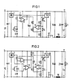
- the storage capacitor 1 is located at the input.
- the positive pole of the input is connected directly to the grounded positive pole of the output.
- the negative pole of the input is led to the negative pole of the output via the drain-source path of the field effect transistor 17 and via the choke 19.
- the filter capacitor 20 At the output is the filter capacitor 20 and, in parallel, the Peltier element 21 as a load resistor.
- the connection point of the field effect transistor to the choke 19 is connected to ground via the freewheeling diode 18 polarized in the passage.
- the control electrode of the field effect transistor 17 is connected to the driver circuit 16.
- the input of the driver circuit 16 is located directly at the output of the comparator 8.
- the comparator 8 is supplied with the comparison voltage U D at its negative input and with the control voltage U ⁇ at its positive input.
- the comparison voltage U D2 is obtained with the aid of an RC arrangement connected to the push-pull output of the square-wave generator 2.
- This RC arrangement is a series circuit consisting of the resistor 3, the parallel circuit consisting of the resistor 4 and the capacitor 5 and the capacitor 6.
- the comparison voltage U D2 is from the connection point of the resistor 3 with the parallel circuit 4, 5 to the Minus entrance of the comparator 8 out.
- the regulator voltage U R passes from the output of the differential amplifier 11 via the resistor 9 to the positive input of the comparator 8.
- the comparator 8 has an open collector output.
- the differential amplifier 11 is a negative feedback operational amplifier.
- the negative feedback resistor 10 is arranged between the output and the negative input.
- the minus input of the differential amplifier 11 is at the tap of the voltage divider consisting of the resistors 12 and 13 and connected to the input voltage U1.
- the plus input of the differential amplifier 11 is connected to a voltage divider which is connected to the input voltage U1 and consists of the temperature sensor 14 and the resistor 15.
- the temperature sensor 14 is a resistor with a negative temperature coefficient.
- the square wave generator 2, the comparator 8, the differential amplifier 11 and the driver circuit 16 are each connected to the input voltage U1 with their supply voltage connections.
- the negative pole of the input voltage U1 is used as the reference potential for the control converter 8, the control comparator 11 and the driver circuit 16.
- a buffer module in CMOS technology is used in particular as driver circuit 16.
- the comparator 8 has the state of high-resistance or HIGH or low-resistance against negative potential - or LOW at the output.
- the square wave generator 2 supplies a square wave voltage with the duty cycle or pulse-pause ratio of approximately 1: 1.
- switch-on potential reaches the control electrode of the field-effect transistor 17 via the resistor 7 and the non-inverting driver circuit 16.
- the output of the comparator 8 is initially high-resistance. If the comparison voltage U D2 exceeds the regulator voltage U R2 , 8 minus potential appears at the output of the comparator. Voltage drops across the load resistor 7, the negative potential passes through the driver circuit 16 to the field effect transistor 17 and blocks it.
- the output voltage U2 can be continuously reduced.
- the switching regulator is intended for temperature control with a Peltier element.
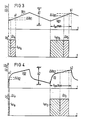
- Fig. 3 shows the input voltage. of the comparator 8 serving as a regulating converter.
- the amplified control deviation or regulator voltage U R1 supplied by the differential amplifier 11 serving as a temperature regulator can change within the working range A1 and "completely sweeps the amplitude of the delta voltage Up 1 at the comparator 8, so that together with the rest Control circuit, the basic values of the output voltage U2 between zero and the half input voltage U1 which results at a duty cycle of 0.5 are entirely possible, but a certain identical change in the regulator voltage U R1 causes, with a small duty cycle at operating point a1, significantly larger percentage changes than with a large duty cycle Working point b1.
- the consequence is instability with low cooling capacity if the gain of differential amplifier 11 has been determined in accordance with the required accuracy for large cooling capacity.
- the comparator 8 starts to work and causes the field effect transistor 17 to be switched off via the resistor 7 and the driver circuit 16. Its switching time is, for. B. approx. 0.4 ⁇ s. That means e.g. B. at an operating frequency of 100 kHz and an input voltage of 9 V that the voltage across the Peltier element 21 jumps suddenly from zero to about 0.35 V. If less power is required, intermittent operation occurs with a period that corresponds to the large thermal time constant. This can e.g. B. are in the range of seconds.
- the regulator voltage oscillates with the appropriate frequency because the measured temperature also fluctuates constantly. Due to a kind of hysteresis, only a significant increase in the cooling capacity required leads to stable operation.
- the excessive sensitivity with a small duty cycle is eliminated by a non-linear course of the comparison voltage at the comparator 8.
- the non-linear comparison voltage U D1 according to FIG. 4 is achieved by connecting the RC element 4, 5 with a small time constant to the integration capacitor 6, on which a largely linear voltage change remains unchanged.
- the resistor 3 serves as a charging resistor for the capacitors 5 and 6.
- the capacitor 5 is charged with a relatively small time constant, given by the time constant of the RC element 3, 5.
- the time constant of the RC element 3, 4, 6 is effective. This time constant is in particular approximately 20 times greater than the smaller time constant of the RC element 3, 5.
- the ratio of the resistors 3 and 4 defines a voltage division from which the amplitude of the voltage across the capacitor 5 results.
- the total voltage or non-linear comparison voltage U D2 enables the gain of the differential amplifier 11 to be optimized, which ensures the required accuracy and stability in the entire working range A2.
- the switching regulator or flow converter according to FIG. 2 largely agrees with that according to FIG. 1 match.
- the resistor 23 instead of the resistor 7, the resistor 23 arranged between the positive pole of the input voltage U E and the input of the driver circuit 16 is provided.
- the additional comparator 22 is provided.
- the additional comparator 22 is located with its negative input at the connection point of the RC parallel circuit 4, 5 with the capacitor 6.
- the positive input of the comparator 22 is located at the output of the rectangular generator 2.
- the voltage of the capacitor 6 which fluctuates around an average value.
- the use of this voltage makes it possible to save a voltage divider for generating an auxiliary voltage.
- Both comparators 8 and 22 are connected to the input voltage U E with their supply voltage inputs. Both comparators 8 and 22 have an open collector output. The parallel connection of the outputs of the comparators is located directly at the input of the driver circuit 16.
- the comparators 8 and 22 have the state of high-resistance or HIGH or low-resistance against negative potential or LOW at the output. If both comparators 8 and 22 have a high impedance at the output, switch-on potential reaches the control electrode of the field effect transistor 17 via the resistor 23 and the driver circuit 16. If one of the two comparators 8 and 22 has a low impedance at its output against negative potential, blocking potential comes through the driver circuit 16 Field effect transistor 17.
- the comparator 22 outputs blocking potential LOW at its output.
- the comparator 22 switches from the LOW state to the HIGH state and switches the field-effect transistor 17 on. This remains switched on until the comparison voltage U D2 at the minus input of the comparator 8 has risen to the value of the regulator voltage U R2 , so that the comparator 8 changes to the LOW state at the output and blocks the field effect transistor.
- the comparison voltage - starting with its minimum value - initially rises steeply in the lower third of the first half-period and then changes into an approximately linear course with a smaller gradient.
- the second half-period begins with a steep decline in the first third, which then changes to a linear area with a smaller negative slope.
- the duration of the first half period is equal to the maximum on time t on max of the electronic switch.
- the percentage change in the duty cycle At / t on is approximately the same for the working points a and b.
- the passive transition of the comparator 22 from LOW to HIGH is inevitably somewhat slower than the active transition of the comparator 8 from HIGH to LOW. This provides compensation in the component itself, which does not depend on additional tolerances of external components.
- the switching regulator shown in FIG. 2 thus enables a continuous power output to the Peltier element without a jump point and starting from the value zero.
- a body is cooled that carries a laser diode.
- the temperature of the cooled body is measured using the temperature-dependent resistor 14. If the temperature of the body to be cooled rises, the value of the resistor 14 becomes smaller and the positive input of the differential amplifier 11 receives a potential shifted towards positive values.
- the negative feedback resistor 10 also raises the potential at the negative input somewhat in the direction of positive voltages.
- the potential at the positive input of the comparator 8 is also shifted in the positive direction, so that more time passes until the comparison voltage U D2 has grown over time to the value of the regulator voltage U R2 and causes the comparator 8 to switch off the switching transistor 17.
- the Peltier element 21 represents a constant load resistance, the output of which is controlled as a function of a temperature.
- the speed of a fan motor is controlled as a function of a temperature or the torque of a DC motor used for drive purposes as a function of the tension of a thread moved by the motor, or the brightness of a lamp is regulated.
Landscapes
- Engineering & Computer Science (AREA)
- Power Engineering (AREA)
- Dc-Dc Converters (AREA)
- Control Of Temperature (AREA)
- Feedback Control In General (AREA)
- Lasers (AREA)
- Control Of Charge By Means Of Generators (AREA)
- Measurement Of Current Or Voltage (AREA)
- Stabilization Of Oscillater, Synchronisation, Frequency Synthesizers (AREA)
Claims (7)
Priority Applications (1)
| Application Number | Priority Date | Filing Date | Title |
|---|---|---|---|
| AT84110881T ATE31233T1 (de) | 1983-09-14 | 1984-09-12 | Schaltregler mit einem komparator, dem eine periodische vergleichsgroesse mit vorgegebenem zeitlichen verlauf zugefuehrt ist. |
Applications Claiming Priority (2)
| Application Number | Priority Date | Filing Date | Title |
|---|---|---|---|
| DE19833333223 DE3333223A1 (de) | 1983-09-14 | 1983-09-14 | Schaltregler mit einem komparator, dem eine periodische vergleichsgroesse mit vorgegebenem zeitlichen verlauf zugefuehrt ist |
| DE3333223 | 1983-09-14 |
Publications (2)
| Publication Number | Publication Date |
|---|---|
| EP0135190A1 EP0135190A1 (fr) | 1985-03-27 |
| EP0135190B1 true EP0135190B1 (fr) | 1987-12-02 |
Family
ID=6209089
Family Applications (1)
| Application Number | Title | Priority Date | Filing Date |
|---|---|---|---|
| EP84110881A Expired EP0135190B1 (fr) | 1983-09-14 | 1984-09-12 | Régulateur à commutation muni d'un comparateur alimenté par une grandeur de comparaison périodique ayant un déroulement temporel donné |
Country Status (5)
| Country | Link |
|---|---|
| US (1) | US4594541A (fr) |
| EP (1) | EP0135190B1 (fr) |
| JP (1) | JPH0753026B2 (fr) |
| AT (1) | ATE31233T1 (fr) |
| DE (2) | DE3333223A1 (fr) |
Families Citing this family (7)
| Publication number | Priority date | Publication date | Assignee | Title |
|---|---|---|---|---|
| GB9005300D0 (en) * | 1990-03-09 | 1990-05-02 | Sunleigh Electrical Developmen | Power supply circuit |
| US5166871A (en) * | 1990-08-31 | 1992-11-24 | International Business Machines Corporation | Buck switching regulator with tow control loops |
| JP2843191B2 (ja) * | 1992-01-30 | 1999-01-06 | 富士通株式会社 | 電子デバイスの駆動回路 |
| US6088251A (en) * | 1999-07-09 | 2000-07-11 | Fedan; Orest | Linearized duty radio, variable frequency switching regulator |
| DE10040413B4 (de) * | 2000-08-18 | 2006-11-09 | Infineon Technologies Ag | Schaltungsanordnung zur Erzeugung eines Schaltsignals für ein stromgesteuertes Schaltnetzteil |
| US7634842B2 (en) * | 2002-07-09 | 2009-12-22 | Santisi Phillip M | Fastening device |
| US11262776B2 (en) | 2019-06-27 | 2022-03-01 | International Business Machines Corporation | Modifying regulator output voltage with a peltier device |
Family Cites Families (6)
| Publication number | Priority date | Publication date | Assignee | Title |
|---|---|---|---|---|
| DE1463553B2 (de) * | 1963-09-19 | 1971-12-16 | Siemens AG, 1000 Berlin u. 8000 München | Schaltungsanordnung zur stabilisierung einer gleichspannung mit einem schalttransistor als stellglied |
| DE2633923C3 (de) * | 1976-07-28 | 1979-08-30 | Siemens Ag, 1000 Berlin Und 8000 Muenchen | Verfahren zum Betrieb eines selbstgetakteten Schaltreglers und Vorrichtungen zur Durchführung des Verfahrens |
| US4096414A (en) * | 1977-05-24 | 1978-06-20 | Cbs Inc. | Dimmer control circuit |
| DE2902463A1 (de) * | 1979-01-23 | 1980-07-24 | Siemens Ag | Schaltungsanordnung zur regelung der ausgangsspannung eines eintakt- durchflussumrichters |
| DE3125528C2 (de) * | 1981-06-29 | 1983-12-29 | TRW Messmer GmbH & Co KG, 7760 Radolfzell | Schaltungsanordnung für einen Schaltregler für induktive Lasten |
| US4459539A (en) * | 1982-07-12 | 1984-07-10 | Hewlett-Packard Company | Charge transfer constant volt-second regulator |
-
1983
- 1983-09-14 DE DE19833333223 patent/DE3333223A1/de not_active Withdrawn
-
1984
- 1984-09-11 US US06/649,319 patent/US4594541A/en not_active Expired - Fee Related
- 1984-09-12 EP EP84110881A patent/EP0135190B1/fr not_active Expired
- 1984-09-12 DE DE8484110881T patent/DE3467959D1/de not_active Expired
- 1984-09-12 JP JP59189859A patent/JPH0753026B2/ja not_active Expired - Lifetime
- 1984-09-12 AT AT84110881T patent/ATE31233T1/de not_active IP Right Cessation
Also Published As
| Publication number | Publication date |
|---|---|
| JPS6077667A (ja) | 1985-05-02 |
| DE3467959D1 (en) | 1988-01-14 |
| ATE31233T1 (de) | 1987-12-15 |
| DE3333223A1 (de) | 1985-03-28 |
| JPH0753026B2 (ja) | 1995-06-05 |
| EP0135190A1 (fr) | 1985-03-27 |
| US4594541A (en) | 1986-06-10 |
Similar Documents
| Publication | Publication Date | Title |
|---|---|---|
| EP0498917B1 (fr) | Convertisseur commandé par horloge avec limitation de courant | |
| EP1316138B1 (fr) | Regulateur de commutation a mode courant | |
| DE102011075008A1 (de) | Controller für einen resonanten schaltwandler | |
| DE69011905T2 (de) | Geschaltete Speisespannungsschaltung mit Anlaufschaltung. | |
| DE19745218A1 (de) | Steuerschaltung und Verfahren zur Steuerung des Schaltens von MOS-Gate-gesteuerten Leistungshalbleiterbauteilen | |
| DE3721075C1 (de) | Gleichspannungsversorgungsschaltung | |
| EP0419724B1 (fr) | Disposition de circuit pour alimentation à découpage du type à récupération | |
| DE2852943A1 (de) | Anordnung mit einem verzoegerungsbehafteten halbleiterschalter | |
| DE19814681A1 (de) | Current-Mode-Schaltregler | |
| DE60006486T2 (de) | Verfahren zur Steuerung eines Halbleiter-Schaltelementes und nach diesem Verfahren gesteuertes Schaltnetzteilgerät | |
| EP0271752A2 (fr) | Convertisseur direct de courant continu | |
| EP0135190B1 (fr) | Régulateur à commutation muni d'un comparateur alimenté par une grandeur de comparaison périodique ayant un déroulement temporel donné | |
| DE4115295C2 (fr) | ||
| DE3841147A1 (de) | Verfahren zum ansteuern eines wechselstrom-motors sowie nach diesem verfahren ansteuerbarer wechselstrom-motor | |
| DE4212472A1 (de) | Freischwingendes Schaltnetzteil | |
| EP0137055B1 (fr) | Dispositif d'alimentation à découpage avec protection contre la surintensité | |
| DE1513420B2 (de) | Spannungsregeleinrichtung zur erzeugung einer geregelten gleichspannung mit einem schalttransistor und einem kontinuierlich gesteuerten stelltransistor | |
| DE69220456T2 (de) | Schaltungsanordnung | |
| DE4008663C1 (fr) | ||
| DE3610156C2 (fr) | ||
| EP0899860B1 (fr) | Etage de sortie de puissance avec opération à modulation de largeur d'impulsion et opération à conduction continue | |
| DE3420312A1 (de) | Ansteuerschaltung fuer einen ablenk-leistungstransistor | |
| EP0024523B1 (fr) | Convertisseur de passage monophasé pour générer des tensions de sortie à courant continu électriquement séparées | |
| DE69314864T2 (de) | Leistungsfaktorkorrekturschaltung | |
| EP0682465B1 (fr) | Circuit pour alimenter des lampes à incandescence |
Legal Events
| Date | Code | Title | Description |
|---|---|---|---|
| PUAI | Public reference made under article 153(3) epc to a published international application that has entered the european phase |
Free format text: ORIGINAL CODE: 0009012 |
|
| AK | Designated contracting states |
Designated state(s): AT BE CH DE FR GB IT LI NL SE |
|
| 17P | Request for examination filed |
Effective date: 19850827 |
|
| 17Q | First examination report despatched |
Effective date: 19860424 |
|
| GRAA | (expected) grant |
Free format text: ORIGINAL CODE: 0009210 |
|
| AK | Designated contracting states |
Kind code of ref document: B1 Designated state(s): AT BE CH DE FR GB IT LI NL SE |
|
| PG25 | Lapsed in a contracting state [announced via postgrant information from national office to epo] |
Ref country code: NL Effective date: 19871202 Ref country code: BE Effective date: 19871202 |
|
| REF | Corresponds to: |
Ref document number: 31233 Country of ref document: AT Date of ref document: 19871215 Kind code of ref document: T |
|
| PG25 | Lapsed in a contracting state [announced via postgrant information from national office to epo] |
Ref country code: SE Effective date: 19871231 |
|
| REF | Corresponds to: |
Ref document number: 3467959 Country of ref document: DE Date of ref document: 19880114 |
|
| ET | Fr: translation filed | ||
| ITF | It: translation for a ep patent filed | ||
| GBT | Gb: translation of ep patent filed (gb section 77(6)(a)/1977) | ||
| NLV1 | Nl: lapsed or annulled due to failure to fulfill the requirements of art. 29p and 29m of the patents act | ||
| PG25 | Lapsed in a contracting state [announced via postgrant information from national office to epo] |
Ref country code: AT Effective date: 19880912 |
|
| PLBE | No opposition filed within time limit |
Free format text: ORIGINAL CODE: 0009261 |
|
| STAA | Information on the status of an ep patent application or granted ep patent |
Free format text: STATUS: NO OPPOSITION FILED WITHIN TIME LIMIT |
|
| 26N | No opposition filed | ||
| PG25 | Lapsed in a contracting state [announced via postgrant information from national office to epo] |
Ref country code: GB Effective date: 19890912 |
|
| GBPC | Gb: european patent ceased through non-payment of renewal fee | ||
| ITTA | It: last paid annual fee | ||
| PGFP | Annual fee paid to national office [announced via postgrant information from national office to epo] |
Ref country code: FR Payment date: 19950919 Year of fee payment: 12 |
|
| PGFP | Annual fee paid to national office [announced via postgrant information from national office to epo] |
Ref country code: DE Payment date: 19951116 Year of fee payment: 12 |
|
| PGFP | Annual fee paid to national office [announced via postgrant information from national office to epo] |
Ref country code: CH Payment date: 19951215 Year of fee payment: 12 |
|
| PG25 | Lapsed in a contracting state [announced via postgrant information from national office to epo] |
Ref country code: LI Effective date: 19960930 Ref country code: FR Effective date: 19960930 Ref country code: CH Effective date: 19960930 |
|
| REG | Reference to a national code |
Ref country code: CH Ref legal event code: PL |
|
| PG25 | Lapsed in a contracting state [announced via postgrant information from national office to epo] |
Ref country code: DE Effective date: 19970603 |
|
| REG | Reference to a national code |
Ref country code: FR Ref legal event code: ST |
|
| REG | Reference to a national code |
Ref country code: FR Ref legal event code: ST |