EP0136008A2 - Scheibenwischersystem mit Steuerung durch Berührung - Google Patents
Scheibenwischersystem mit Steuerung durch Berührung Download PDFInfo
- Publication number
- EP0136008A2 EP0136008A2 EP84305193A EP84305193A EP0136008A2 EP 0136008 A2 EP0136008 A2 EP 0136008A2 EP 84305193 A EP84305193 A EP 84305193A EP 84305193 A EP84305193 A EP 84305193A EP 0136008 A2 EP0136008 A2 EP 0136008A2
- Authority
- EP
- European Patent Office
- Prior art keywords
- output
- wiper
- input
- actuation
- actuating
- Prior art date
- Legal status (The legal status is an assumption and is not a legal conclusion. Google has not performed a legal analysis and makes no representation as to the accuracy of the status listed.)
- Withdrawn
Links
- 230000004044 response Effects 0.000 claims description 5
- 230000009849 deactivation Effects 0.000 claims description 3
- 239000012530 fluid Substances 0.000 claims description 3
- 238000004140 cleaning Methods 0.000 claims description 2
- 230000010355 oscillation Effects 0.000 claims description 2
- 230000000994 depressogenic effect Effects 0.000 abstract description 11
- 230000000977 initiatory effect Effects 0.000 abstract description 5
- 239000003990 capacitor Substances 0.000 description 16
- 239000003595 mist Substances 0.000 description 12
- 238000010586 diagram Methods 0.000 description 5
- 230000009471 action Effects 0.000 description 4
- 230000001105 regulatory effect Effects 0.000 description 3
- 230000008859 change Effects 0.000 description 2
- 230000001934 delay Effects 0.000 description 2
- 238000001035 drying Methods 0.000 description 2
- 230000000694 effects Effects 0.000 description 2
- 230000007246 mechanism Effects 0.000 description 2
- 230000004048 modification Effects 0.000 description 2
- 238000012986 modification Methods 0.000 description 2
- 230000006978 adaptation Effects 0.000 description 1
- 230000003534 oscillatory effect Effects 0.000 description 1
Images


Classifications
-
- B—PERFORMING OPERATIONS; TRANSPORTING
- B60—VEHICLES IN GENERAL
- B60S—SERVICING, CLEANING, REPAIRING, SUPPORTING, LIFTING, OR MANOEUVRING OF VEHICLES, NOT OTHERWISE PROVIDED FOR
- B60S1/00—Cleaning of vehicles
- B60S1/02—Cleaning windscreens, windows or optical devices
- B60S1/46—Cleaning windscreens, windows or optical devices using liquid; Windscreen washers
- B60S1/48—Liquid supply therefor
- B60S1/481—Liquid supply therefor the operation of at least part of the liquid supply being controlled by electric means
- B60S1/482—Liquid supply therefor the operation of at least part of the liquid supply being controlled by electric means combined with the operation of windscreen wipers
Definitions
- This invention relates to a control for a windshield wiper system on a motor vehicle. It particularly relates to such a control with a minimum number of easily operated control actuators which control multiple modes of system operation.
- the invention relates to a windshield wiper drive control apparatus having a pair of single touch actuators, one of which initiates windshield wiper action with a first touch and toggles back and forth between two modes of windshield wiper operation, such as high speed and low speed, with additional touches.
- the second actuator turns the windshield wiper system off if touched while the windshield wiper system is operating and causes a single wipe cycle of the windshield wipers if touched while the system is not operating.
- Further windshield wiper control functions may be added with additional single touch operators, such as, for example, an additional actuator to initiate and control intermittent or delay windshield wiper operation with control of delay time and yet another single touch operator to initiate, alternatively, preprogrammed or operator controlled windshield washer operation.
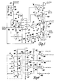
- a windshield 2 of a motor'vehicle is cleaned by a pair of wiper blades 3 and 4 which clean an area of windshield 2 defined by the broken lines.
- Blades 3 and 4 are driven through a linkage 5 by a motor 6 which, in this embodiment, is a three brush, permanent magnet motor.
- motor 6 could alternatively be a DC wound field motor or any other suitable motor.
- motor 6 and linkage 5 could be replaced by a pair of motors, one driving each wiper blade, the motors being linked mechanically or electrically to act in unison.
- Motor 6 or linkage 5 has associated therewith an inner wipe switch 7, actuated by a cam when the wipers reach an inner wipe position that defines the lower end of their normal wipe cycle.
- an inner wipe switch 7 actuated by a cam when the wipers reach an inner wipe position that defines the lower end of their normal wipe cycle.
- this is also a park position for wipers 3 and 4 when not in use.
- a lower park position is defined.
- First actuating means 10 and second actuating means 12 are identical single-pole, single- throw switches of the momentary contact type; preferably touch or pushbutton operated and located on the dashboard or some other portion of the vehicle passenger compartment within easy reach of the vehicle operator.
- the first and second actuating means appear to the operator as the upper two touch pads of a dash switch unit 9, as seen in Figure 2, with the first actuating means 10 labelled LO/HI and the second actuating means 12 labelled MIST/OFF.
- Two other touch pads 11 and 13, labelled WASH and DELAY, respectively, are shown in Figure 2 and will be described at a later point in the specification.
- First actuating means 10 provides an output to a set (S) input of first bistable electronic circuit means 14, which has a reset (R) input effective to receive an output from the second actuating means 12.
- a Q output of first bistable electronic circuit means 14 is provided to one input of an OR gate 15 having an output connected to the input of an AND gate 16.
- the output of the second actuating means 12 is provided to a set (s) input of a second bistable electronic circuit means 17 having a Q output connected to the other input of OR gate 15.
- first actuating means 10 is provided to a CLK input of a third bistable electronic circuit means 18 having a Q output connected to the other input of AND gate 16 and a Q output connected to actuate high speed drive 19 which, when actuated, connects an electric power supply 20, which may be the vehicle battery or alternator, through ignition switch 24 to a high speed brush of motor 6.
- the output of AND gate 16 connects to one input of an OR gate 21, the output of which is connected to actuate low speed drive 22.
- Low speed drive 22 when actuated, connects electric power supply 20 to a low speed brush of motor 6 through ignition switch 24.
- Third bistable electronic circuit means 18 has a reset (R) input actuated by the second actuating means 12. Further, it incorporates elements effective to prevent a change in its output after it is reset until the second actuation of the CLK input by the first actuating means 10. The second and subsequent actuations of the CLK input cause reversals of its output state.
- the second bistable electronic circuit means 17 has a reset (R) input connected to a regulated voltage +V, as described further in Figure 3, through inner wipe switch 7 so as to be reset when the wipers 3 and 4 are not in their inner wipe position.
- cycle finish means 23 provides an output to the other input of OR gate 21 and will be described in greater detail below.
- closure of the vehicle ignition switch causes connection of the circuit as shown in Figure 1-with all bistable electronic circuit means or bistable means 14, 17 and 18 reset, with Q outputs low_and g outputs high.
- Neither low speed drive 22 nor high speed drive 19 is actuated; and wipers 3 and 4 are parked with the inner wipe switch open.
- wipers 3 and 4 are parked in the inner wipe position.
- wipers 3 and 4 are parked in a lower park position, but the cam is sufficiently wide to maintain the inner wipe switch open from the inner wipe to the park position.
- first bistable means 14 When first actuating means 10 is first actuated, first bistable means 14 is set and the Q output of third bistable means 18 remains high. Thus low speed drive 22 is actuated and wipers 3 and 4 are cycled continuously. Another actuation of first actuating means 10 toggles third bistable means 18 to a second state with output Q low and output Q high. Thus low speed drive 22 is deactivated and high speed drive 19 actuated. Further actuations of first actuating means 10 cause further reversals in the output state of third bistable means 18 with resultant switching between low speed drive 22 and high speed drive 19.
- cycle finish means enables the low speed drive to drive the wipers in the low speed mode to their park position.
- cycle finish means 23 may comprise the output of the inner wipe switch 7.
- the cycle finish means is a mechanical latch that holds a relay armature closed after the actuating coil is deactivated until the wipers reach the park position, as shown and described, for example, in the United States patent to Romanowski 3,253,206, issued May 24, 1966.
- a single wipe cycle may be initiated by actuating second actuating means 12.
- second bistable means 17 resets, but cycle finish means 23 takes over to complete the cycle. This provides the mist feature useful for cleaning a slight mist from the windshield with a single wipe of the blades.
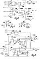
- a depressed park embodiment of the system is described in detail, beginning with Figure 3.
- a main control chip 25 could be a properly programmed digital computer; however, in this embodi- - ment it is a custom designed digital logic control system on a single chip.
- the various inputs and outputs to chip 25 are labelled in the drawing and their connections to further circuit apparatus are shown. Electrical power from the vehicle electrical power supply is provided through the vehicle ignition switch, a resistor 27, the collector and emitter of an NPN transistor 28 and a diode 29 to the VDD input of chip 25, which input is also connected through a capacitor 30 to ground.
- the collector of transistor 28 is further connected through a Zener diode 31 to ground and also through a resistor 32 to the base of transistor 28, which base is connected through a Zener diode 33 to ground.
- Elements 27 through 33 comprise a regulated power supply for chip 25 with a comparatively large storage capacitor 30 effective to continue to provide power to chip 25 for a predetermined period of time after the vehicle ignition switch is opened.
- the emitter of transistor 28 is further connected to ground through a capacitor 35 and, through a diode 36, to an ignition or IGN input of chip 25.
- This input provides an ignition signal to the chip 25 so that the chip 25 knows when the ignition has been turned off even though power is still being supplied thereto.
- the emitter of transistor 28, at which regulated voltage +V is generated, is further connected through the inner wipe switch 7 to the IW input of chip 25, which input is further connected through a resistor 39 to ground.
- This input provides chip 25 with information as to the state of the inner swipe switch 7.
- Chip 25 further has two oscillator inputs, OSC 1 and OSC 2, which are connected to each other through a resistor 40 with OSC 1 further connected to a capacitor 41 to ground.
- Chip 25 includes an on-chip oscillator which uses the external capacitor 41 and resistor 40 to help determine the period of oscillation.
- Another input to chip 25 is the multiplex or MUX input which is connected through a resistor 42 to the junction 43 of a resistor 44 and a capacitor 45. Junction 43 is connected to the dash switch input, to be described at a later point in this specification, and further, through resistor 44 to the IGN input of chip 25 and through capacitor 45 to ground. Finally, input VSS connects to ground.
- the LO output connects to the base of an NPN Darlington transistor 47 having a grounded emitter and a collector connected to an actuating coil 48 of a relay 49 and a parallel, free wheeling diode 50.
- the other end of actuating coil 48 is further connected through an armature 51 of relay 49 to the low speed brush of motor 6 and through an armature 53 of a relay 54 to the vehicle ignition switch.
- Actuating coil 55 of relay 54 has one end grounded and the other end connected to the collector of a PNP transistor 56, which has its emitter connected to the vehicle ignition switch and, through a resistor 57, to its own base.
- the base of transistor 56 is connected through a resistor 58 to the collector of an NPN Darlington transistor 59 having a grounded emitter and a base connected to the PK output of chip 25.
- the collector of transistor 59 is further connected through a back-biased diode 60 to ground.
- the HI output of chip 25 is connected through a capacitor 63 to the base of an NPN transistor 64 having a grounded emitter.
- the base of transistor 64 is further connected through a - resistor-65 to ground; and the collector of transistor 64 is connected through a capacitor 66 to ground and further through a resistor 67 to the collector of transistor 28.
- the collector of transistor 64 is also connected through a resistor 68 to the base of an NPN Darlington transistor 69 having a grounded emitter.
- the base of transistor 69 is connected through a resistor 70 to ground; and the collector is connected through a back-biased diode 71 to the collector of transistor 59 and through a diode 72 and parallel actuating coil 73 of a relay 74 to the ignition switch 1GN, which itself is connected through an armature 75 of relay 74 to the high speed brush of motor 6.
- the WSH output of chip 25 is connected to the base of a grounded emitter, Darlington NPN transistor 76 having a collector connected through a standard washer pump motor 77 to the ignition switch.
- a Zener diode 62 is connected across the collector and emitter of transistor 76.
- a high output from output PK of chip 25 actuates transistors 59 and 56 to cause relay armature 53 to pull closed and thereby provide a connection between the ignition switch and the armature of relay 49.
- a high output from the LO output of chip 25 will actuate relay 49 to connect ignition voltage to the low speed brush and actuate the wipers at low speed.
- Relay 54 is of the type previously mentioned as described in the U.S. patent 3,253,206. It includes mechanical latch apparatus to remain closed until coil 55 is deactivated and wipers 3 and 4 reach their park positions.
- the HI output of chip 25 could be connected directly to the base of transistor 69 - so that a high output thereon would actuate relay 74 to connect ignition to the high speed brush.
- chip 25 generates an oscillating output on the HI output while high speed operation is not desired.
- This oscillating output cycles transistor 64 on and off to repeatedly discharge capacitor 66, which is being continually charged from the ignition through the resistors 27 and 67.
- capacitor 66 is allowed to charge and eventually turns on transistor 69 to actuate relay 74 and connect ignition voltage to the high speed brush for high speed wiper operation.
- transistor 69 turns on, diode 71 causes transistor 56 to turn on if it is not already on and thereby actuate relay 54.
- This circuit arrangement provides for automatic selection of high speed wiper operation if chip 25 should fail while the ignition is on.
- the opening of the ignition switch with the wiper system operating will result in the wipers stopping immediately at whatever point in their pattern they happen to occupy.
- the alternative connection of the armature 53 of relay 54 to battery potential bypassing the ignition switch would have the effect that, when the ignition is turned off, relay 54 would remain closed and the wipers.would continue to operate at low speed.
- Logic circuitry could be provided to continue such operation until the desired park position is reached, at which point the system would turn the wipers off. If, for some reason, the wipers were mechanically prevented from returning to the park position, such operation would continue only as long as the short-term keep alive power supply continued to power chip 25.
- chip 25 has a single MUX input for the control switches and a single input line from the dash switch assembly.
- Figure 4 shows the dash switch circuit and the electronics and logic internal to chip 25 which are required to voltage-multiplex the dash switch signal. From the chip IGN input, a circuit can be traced through resistor 44, line 46, resistor 78, resistor 79, resistor 80 and the collector and emitter of an NPN transistor 81 to ground. The base of transistor 81 is connected to ground through MIST/OFF switch 12 and is also connected through a resistor 82 to the junction of resistors 44 and 78, which junction is also connected to ground through LO/HI switch 10.
- resistors 78 and 79 are connected to ground through WASH switch 11; and the junction of resistors 79 and 80 is connected to ground through DELAY switch 13.
- Elements 10, 11, 12, 13, 78, 79, 80, 81 and 82 are all included within the dash switch unit 9, which is connected to the rest of the washer apparatus through line 46 and a common ground and which generates on line 46 a voltage which is a fraction of the ignition voltage, the fraction depending on which of the switches is closed.
- Resistors 44, 78, 79 and 80 have resistance values forming a ratio such as 3:1:2:6 so that closure of the switches numbered 10, 11 or 13 results in a voltage on line 46 which is 0%, 25% or 50% of the ignition voltage, respectively.
- resistor 82 depends in part on the characteristics of transistor 81; but in any case it is chosen to be sufficiently large that, if MIST/OFF switch 12 is closed, the voltage on line 46 is only slightly less than the voltage appearing at the IGN input of chip 25. Resistor 82 further ensures that, if no switch is closed, transistor 81 will conduct; and the voltage on line 46 will be approximately 75% of the chip IGN voltage.
- resistors 83, 84, 85, 86 and 87 form a series of voltage dividers between the IGN input and ground.
- the resistance ratio of these resistors is 1:2:2:2:1.
- the junctions of these resistors are connected to the inverting inputs of operational anplifiers (op amps) 88,89,90 and 91, respectively.
- the outputs of these op amps are connected to chip input VDD through identical resistors, which are given the common reference 92, with the result that these op amps act as comparators.
- the non-inverting inputs of each of the op amps are all connected to the MUX input of chip 25, which is in turn connected through resistor 42 to line 46.
- the output of comparator 88 provides a M/OFF signal within chip 25. It is further provided through an inverter 93 to one input of an AND gate 94. The output of comparator 89 is provided to the other input of AND gate 94 to provide a NO SWITCH signal therefrom within chip 25. The output of comparator 89 is further provided through an inverter 95 to one input of an AND gate 96, which receives at its other input the output of comparator 90 and which provides, at its output, a DELAY signal within chip 25. The output of comparator 90 is further provided through an inverter 97 to one input of an AND gate 98, which receives at its other input the output of comparator 91 and which generates at its output a WASH signal within chip 25. Finally, the output of comparator 91 is supplied through an inverter 99 to generate a LO/HI signal within chip 25.
- resistors 44 and 82 form a voltage divider across the chip IGN voltage; and, since resistor 82 is much greater than resistor 44 (in the ratio of, for example, 200:3), a voltage is provided to the non-inverting inputs of each of the comparators which causes all the outputs to go high. These high outputs are inverted to low signals by each of the inverters 93, 95, 97 and 99; but the high output of comparator 88 provides a high M/OFF signal within chip 25. If no switch is closed, transistor 81 conducts so that resistors 44, 78, 79 and 80 form a voltage divider across the chip IGN voltage.
- the voltage on line 46 is approximately 75% of the chip IGN voltage, which is sufficient to provide a high output from comparators 89, 90 and 91 and a low output from comparator 88.
- AND gate 94 receives a high input through inverter 93 from the low output of comparator 88 and a high input from comparator 89 to generate a high NO SWITCH signal within chip 25.
- Inverters 95, 97 and 99 each provide low output signals to ensure that no other high signals are generated. In view of the preceding description, there should be no need to describe in detail the actuation of WASH switch 11 or DELAY switch 13.
- Each of the five signal outputs of Figure 4 is processed with suitable debounce circuitry similar to that shown in Figure 10, to be described at a later point in this specification.
- the debounced LO/HI and DELAY signals are provided to the two inputs of an OR gate 101 having an output connected to the S input of an RS monostable multivibrator (flip flop) 102.
- the Q output of flip flop 102 is provided to one input of an OR gate 103 having an output connected to one input of an AND gate 104.
- the output of AND gate 104 is the PK signal applied to the PK output of chip 25.
- a power-on-reset (POR) signal and the debounced M/OFF signal are provided to the two inputs of an OR gate 105 having an output connected to the reset (R) input of flip flop 102.
- the debounced M/OFF signal is further provided to the set (S) input of an RS flip flop 106 having a Q output connected to another input of OR gate 103.
- the third and last input to OR gate 103 is a signal labelled CLRDC which is obtained from the apparatus shown in Figure 8.
- the reset (R) input of flip flop 106 receives a signal labelled ZX, which is obtained from the apparatus shown in Figure 9.
- the POR signal is obtained from the circuit shown in Figure 6.
- the debounced LO/HI signal is applied to one input of an AND gate 108 and also through an inverter 109 to the CK input of an D flip flop 110.
- the D input of flip flop 110 is connected - to input VDD of chip 25; and the Q output is connected to the other input of the AND gate 108.
- the output of AND gate 108 is connected to the CK input of a toggle flip flop 111 having a T input connected to input VDD of chip 25.
- the debounced DELAY signal and the output of OR gate 105 are connected to the two inputs of an OR gate 112 having an output connected to the reset (R) inputs of flip flops 110 and 111.
- the Q output of flip flop 111 and the IGN signal are connected to the two inputs of an AND gate 113 having an output labelled ALT HI, which is an optional output for chip 25 which may be connected directly to the base of transistor .69 in Figure 3 as previously described.
- the Q output of flip flop 111 is connected to one input of AND gate l14 and one input of AND gate 115.
- AND gate 114 generates at its output the LO signal applied to the LO output of chip 25 and has as further inputs the IGN signal and a signal labelled MM, which is obtained from the apparatus in Figure 9.
- AND gate 115 generates at its output the HI signal connected to the HI output of chip 25 and includes as a further input the CLK or clock signal generated by the clock oscillator circuit of Figure 7.
- Flip flop 102 of Figure 5 corresponds to the first bistable means 14 of Figure l. Actuation of LO/HI switch 10 or DELAY switch 13 sets the Q output of flip flop 102 high to generate a high PK signal, as long as the ignition switch is closed, and thereby actuate run relay 54 of Figure 3. Actuation of LO/HI switch 10 further provides a high signal to one input of AND gate 108; but the other input receives a low Q output from flip flop 110, which was previously reset by the POR signal and has not yet received a positive edge trigger on its CK input.
- Release of LO/HI switch 10 provides this trigger through inverter 109 to set output Q of flip flop 110 high but removes the high signal from the one input of AND gate 108 so that flip flop 111 remains reset with low Q and high Q outputs.
- a high LO signal on gate 114 is provided to actuate relay 49 of Figure 3 and connect a circuit to the low speed brush of motor 6 in Figure 1 through relays 49 and 54 of Figure 3.
- AND gate 115 is enabled to pass the CLK pulses of the HI signal to prevent the actuation of relay 74 for the high speed brush.
- the ALT HI signal is also low.
- flip flop 106 is set to a high Q output to actuate relay 54 and initiate low speed wiper movement. As soon as the wipers move far enough to close the inner wipe switch, relay 106 is preset by signal ZX; but relay 54 is now latched closed and wiper operation continues for a single cycle and back to the park position.
- FIG. 11 an adaptation of the system of Figures 1, 3 and 5 to a non-depressed park wiper apparatus is shown.
- the apparatus of Figure 11 replaces relays 49, 54 and 74 of Figure 3 together with associated drive circuitry through Darlington transistors 47, 59 and 69.
- An AND gate 185 receives the PK and LO signals as inputs.
- An AND gate 186 receives the LO and IW signals as inputs.
- An OR gate 187 receives as inputs the ALT HI signal (or is connected to the junction of resistors 68 and 70) and the outputs of AND gates 185 and 186 and provides an output to the base of a grounded emitter NPN power transistor 188.
- the collector of transistor 188 is connected to the ignition switch through the actuating coil 189 of a relay 190 having an armature 191 connected to the low speed brush of motor 6 and actuable from a normally closed contact 192, which is grounded, to a normally open contact 193.
- Another grounded emitter NPN transistor 194 has a base supplied with the ALT HI signal (or connected to the junction of resistors 68 and 70) and a collector connected to the ignition switch through the actuating coil 195 of a relay 196 having an armature 197 connected to the high speed brush of motor 6 and actuable from a normally closed contact 198, connected to contact 193 of relay 190, to a normally open contact 199 connected to the high speed brush of motor 6.
- FIG. 7 further shows a NAND gate 118 having a first input connected to the OSC 1 input of chip 25, a second input connected to the IGN input of chip 25 and an output connected to the OSC 2 input of chip 25.
- resistor 40 With an ignition or IGN signal applied to the IGN input of chip 25, resistor 40 provides positive feedback around NAND gate 118 to generate an oscillatory square wave output at a frequency determined by the RC combination of resistor 40 and capacitor 41.
- the power-on-reset or POR signal is generated in the circuit of Figure 6.
- the VDD input of chip 25 is connected through a resistor 120 in series with a parallel resistor 121 and capacitor 122 to ground.
- the common junction 123 of these elements provides the POR signal through an inverter 124.
- inverter 124 temporarily generates a high POR signal until capacitor 122 can charge up sufficiently to send the output of inverter 124 low. This provides a brief high signal at the initiation of system operation which is used to reset a plurality of devices within the apparatus shown in Figures 5-10. As an example, all four flip flops of Figure 5 are reset by this signal, as will be apparent in the later description of the apparatus of Figure 9.
- Figure 8 shows the apparatus actuated by the WASH signal and effective to control washer and wiper operations during the programmed and operator controlled washer modes of operation of the system.
- the WASH signal is provided to the CK input of a D flip flop 130 having a D input connected to input VDD of chip 25 and a Q output connected to one input of an AND gate 131.
- AND gate 131 has further inputs receiving an IW signal from the apparatus of Figure 10 and the CLK signal from the apparatus of Figure 7.
- the output of AND gate 131 is provided to a CK input of a counter 132 having a QN bit output connected to one input of an QR gate 133, the output of which is connected to a reset or R input of flip flop 130.
- QN is a designation for a predetermined one of the outputs Ql, Q2, Q3, etc.
- Output Q of flip flop 130 is further connected to one input of an AND gate 134 having another input receiving the IW signal from the apparatus of Figure 10 and an output connected to one input of OR gate 135.
- the output of OR gate 135. is connected to one input of an AND gate 136 which has further inputs receiving the IGN signal from chip 25 and a timed inhibit signal from apparatus not shown.
- the output of AND gate 136 is connected to the WSH output of chip 25 to actuate the washer pump motor 77.
- the timed inhibit input to AND gate 136 is an optional input from a timer which is initiated by the actuation of washer switch 11 and which switches low after a predetermined maximum wash time to protect the washer motor from overuse, if such protection is thought advisable. This time limit would not be reached in normal operation of the circuit.
- the Q output of flip flop 130 is further provided to - one input of an OR gate 137 which provides at its output a signal labelled CLRDC, which signal is provided to OR gate 103 of Figure 5 to generate the run signal PK.
- the debounced wash signal is applied to one input of an AND gate 138 having an output connected to the CK input of a counter 139.
- a debounced WASH-signal is connected to the clear or CLRinput of counter 139; and the CLK signal from Figure 7 is provided to another input of AND gate 138.
- the QN output of counter 139 is provided to one input of OR gate 135, one input of OR gate 137, one input of OR gate 133 and, through an inverter 140, to the last input of AND gate 138.
- the QN bit of counter 139 is selected such that, in combination with the clock frequency of the system, it goes high after approximately one second of actuation of the wash switch 11.
- flip flop 130 is reset but the WSH and CLRDC signals are both maintained high independently of flip flop 130 as long as the wash switch 11 remains closed.
- Inverter 140 provides a low signal to remove AND gate 138 from control; however, output ON remains high until the WASH signal clears counter 139.
- flip flop 130 and counter 132 provide programmed wash duration control; however, if wash switch 11 is closed for longer than one second, counter 139 provides for washer operation as long as the operator holds WASH switch 11 closed.
- the wipers run for a predetermined number of cycles after the cessation of fluid delivery to the windshield to clear the excess fluid from the viewing area.
- the Q output of flip flop 130 and the QN bit output of counter 139 are both supplied as inputs to a NOR gate 142 having an output connected to the CK input of a D flip flop 143.
- the Q output of flip flop 143 is provided to the third input of OR gate 137 so as to provide for continued low speed wiper operation when set hi h.
- the Q output is further provided to an OR gate 144 having an output connected to the reset input of counter 132.
- NAND gate 145 the other input of which receives the IW signal from the apparatus of Figure 10.
- the output of NAND gate 145 is provided to the CK Lnput of a counter 146 having a reset input connected to the Q ⁇ output of flip flop 143 and a ON bit output connected to one input of an OR gate L47.
- the output of OR gate 147 is provided to :he input of another OR gate 148 having an output connected to the reset input of flip flop 143.
- the D input of flip flop 143 is connected to input VDD of chip 25.
- NOR gate 142 In operation, when flip flop 130 and counter 139 are both reset, NOR gate 142 generates a high output to set flip flop 143 with a high Q output and a low Q output. The high Q output causes continued wiper operation in low speed through the CLRDC signal, resets counter 132 through OR gate 144 and actuates NAND gate 145 to provide a clock pulse to counter 146 with every open-to-closed transition-of the inner wipe switch 38. When the required number of cycles of switch 38 have occurred, the QN output of counter 146 causes a reset of flip flop 143 through OR gates 147 and 148 to end wiper operation in the wash mode.
- OR gate 147 is further provided with inputs of the debounced M/OFF signal and the POR signal.
- the output of OR gate 147 is provided to the other input of OR gate 144 and also to the last input of OR gate 133 to reset both flip flop 130 and counter 132 in response to the M/OFF or POR signals.
- a D flip flop 149 receives a clock or CK input from the debounced WASH signal and has a D input connected to input VDD of chip 25, a reset or R input from a lower bit output such as Q2 of counter 132 and a Q output connected to the other input of OR gate 148.
- the Q output of flip flop 149 is set high briefly between the initial actuation of wash switch 11 and the high output from the Q2 bit output of counter 132 to. cause the cessation of the windshield drying cycle - controlled by flip flop 143 and counter 146 in the event that the wash switch 11 is reactuated during this drying cycle.
- Figure 9 shows the apparatus devoted to the control of the delay or intermittent mode of wiper operation.
- An OR gate 150 has an output labelled MM, which is provided to an input of AND gate 114 in Figure 5. This output must be high for low speed wiper operation to be enabled.
- OR gate 150 has four inputs: one receiving the signal CLRDC from OR gate 137 in Figure 8; one from the Q output of a D flip flop 151; one from the output of an AND gate 152; and one from the Q output of a D flip flop 153.
- the CLRDC signal enables low speed wiper operation as required by the wash modes, as previously described. The function of the other three inputs will be described below.
- the debounced LO/HI and M/OFF signals are provided to the inputs of an OR gate 154 having an output connected to the clear or CLR input of flip flop 153.
- the debounced DELAY signal is applied to the CK input of flip flop 153, the D input of which is connected to input VDD of chip 25.
- the Q output of flip flop 153 is connected to one input of AND gate 152.
- actuation of the LO/HI switch 10 or the MIST/OFF switch 12 will clear flip flop 153 to provide a high Q output and thereby generate a high MM signal.
- DELAY switch 13 will clock flip flop 153 to generate a high Q output and thereby provide a high input to one input of AND gate 152.
- the other input of AND gate 152 is controlled by the delay circuit of Figure 9 to generate intermittent high MM signals and thus intermittent low speed wiper operation.
- the delay system of Figure 9 is a one switch, two touch system in which the first actuation of the delay switch initiates a single wipe of the wipers followed by a delay with a counter counting. A second touch of the delay switch stops the counter, initiates a second wipe of the wipers and causes repeated alternating delays and wipes with the delays controlled by the count of the counter.
- a toggle flip flop 155 obtains the debounced DELAY signal at its CK input and has a CLR input connected to the output of an OR gate 156 having one input connected to the output of the OR gate 154.
- the toggle or T input of flip flop 155 is connected to input VDD of chip 25.
- Flip flop 155 is normally cleared to a high Q output by actuation of LO/HI switch 10 or MIST/OFF switch 12. Actuation of delay switch 13 will cause flip flop 155 to toggle to its alternate state with a high Q output; while a second actuation of the delay switch 13 causes a toggle back to the high Q output state. Thus, a high Q output from flip flop 155 signals the delay setting mode.
- counting means are provided which in this embodiment are shown as a pair of counters 160 and 161.
- the input and output of these counters are described as those of the CD4516B presettable binary up/down counter, although other counting means could be substituted as desired.
- the counters are cascaded with the CI or carry in input of counter 160 grounded and the CO or carry out output of counter 160 connected to the CI input of counter 161.
- the clock or CK inputs of both counters are connected to the output of an AND gate 162 having one input receiving the CLK clock signal and the other input connected to the Q output of flip flop 155, so that a high Q output from flip flop 155 causes counters 160 and 161 to count the CLK clock pulses.
- the U/D or UP/DOWN inputs of counters 160 and 161 are both connected to input VDD of chip 25 so that the counters count up only.
- the reset or R inputs, as well as the preset or PO-P3 inputs of counters 160 and 161 are all grounded so that a preset enable causes the counters to begin counting upward from zero.
- the PE or preset enable inputs of counters 160.and 161 are both connected to the output of an AND gate 163 having one input connected to the Q output of flip flop 155.
- the other input of AND gate 163 receives the output of an OR gate 164 having an input from the output of an OR gate 165.
- OR gate 165 receives a POR signal from the circuit of Figure 6 on one input and the IW signal from the circuit of Figure 10 on the other input.
- counters 160 and 161 receive clock pulses whenever the high Q' output state exists in flip flop 155, they are not released to count from their zero preset unless inner wipe switch 7 is open.
- Apparatus may be provided to initiate a single wipe of the wipers at the beginning of the delay set mode, but the time count will not begin until the end of this single wipe.
- Apparatus to provide such a single wipe includes a D flip flop 166 having a CK input connected to the Q output of flip flop 155, a D input connected to input VDD of chip 25, a CLR input connected to the output of OR gate 165 and a Q output connected to one input of an OR gate 167, the output of which is connected to the other input of AND gate 152.
- the apparatus is provided with a default count limit for counters 160 and 161.
- the CO outputs of both counters 160 and 161 are provided to the input of'a NOR gate 168 having an output connected to the CK input of a D flip flop 169.
- Flip flop 169 has a D input connected to input VDD of chip 25 and a Q output connected to the other input of OR gate 156.
- Another feature of this delay circuit is that, if the operator actuates the wash switch or turns the vehicle ignition off and then on again after initiating the delay set mode with the first actuation of delay switch 13 but before completing the delay set, counters 160 and 161 are cleared to zero for automatic resumption of the delay set mode at the end of the wash cycle or when the ignition is once again turned on.
- This is accomplished by the provision of the CLRDC signal from the apparatus of Figure 8 to another input of OR gate 164 and the provision of a IGN signal, which may be obtained through an inverter from the IGN signal, to a third input of OR gate 164.
- a IGN signal which may be obtained through an inverter from the IGN signal
- a second pair of counters 170 and 171 is provided. These counters have their reset or R and U/D inputs grounded. They are also cascaded with the CI input of counter 170 grounded and the CI input of counter 171 connected to the CO output of counter 170.
- Counter 170 has-its preset or PO-P3 inputs connected to the QO-Q3 outputs of counter 160; and counter 171-similarly has its PO-P3 inputs connected to the QO-Q3 outputs of counter 161.
- the CK inputs of both counters 170 and 171 receive the output of an AND gate 172 having four inputs: the Q output of flip flop 155; the CLK signal from the apparatus of Figure 7; the IW signal from the apparatus of Figure 10; and the output of a NOR gate 173 through an inverter 174.
- NOR gate 173 has one input from the CO output of counter 171, a second input from the CO output of counter 170 and a third input from the Q output of flip flop.155.
- the output of NOR gate 173 is further provided as another input to OR gate 167.
- the PE inputs of counters 170 and 171 are both connected to the output of AND gate 175 having one input connected to the Q output of flip flop 155 and the other input connected to the output of OR gate 165.
- the counters act as down counters, counting downward toward zero from whatever preset value is loaded into input PO-P3 by the PE signal.
- the counters count the CLK pulses, but only in conjunction with a high Q output from flip flop 155, an open inner wipe switch 7 and CO outputs from counters 170 and 171 indicating that the counters have not yet reached zero.
- the counters 170 and 171 are enabled to load the preset values while the inner wipe switch 7 is closed and the flip flop 155 has a high Q output.
- the actual counting begins when the inner wipe switch 7 opens at the end of a wipe cycle of wipers 3 and 4.
- a D flip flop 176 is provided to initiate a single wipe after the second actuation of delay switch 13.
- Flip flop 176 has a CK input connected to the Q output of flip flop 155, a CLR input connected to the output of OR gate 165 and a Q output connected to the fourth and final input of OR gate 167.
- the toggling of flip flop 155 to its high Q state clocks flip flop 176 to generate a high output, which causes a high MM signal for the initiation of low speed wiper operation.
- flip flop 176 is cleared to a low Q output; however, wiper operation is continued through the connection of the signal IW to OR gate 167.
- the opening of inner wipe switch 7 at the end of a single wipe sends signal MM low to stop the wipers in the inner wipe position and begin the count down of counters 170 and 171 from the count loaded in from counters 160 and 161.
- NOR gate 173 When the count on counters 170 and 171 reaches zero, NOR gate 173 generates a high output to both stop the application of clock pulses to counters 170 and 171 through AND gate 172 and to generate a high MM signal once again through OR gate 167.
- the count from counters 160 and 161 is once again loaded into the preset inputs of counters 170 and 171; and the cycle repeats in this manner until the operator takes some action to discontinue the delay operation.
- a debounce circuit for the system of Figures 5-10 is shown in Figure 10.
- This circuit is shown in particular for the inner wipe switch 7, but a similar debounce circuit may be provided for each of the switches which need to be debounced.
- the inner wipe switch 7 and resistor 39 to ground are repeated for clarity, with the junction between the two, as seen in Figure 3, corresponding to the IW input to chip 25.
- This junction is connected to one input of an AND gate 180 having another input receiving the CLK signal from the apparatus of Figure 7.
- the output of AND gate 180 is provided to the CK input of a counter 181 having a QN output providing the debounced IW signal, from which the debounced IW signal can be generated through an inverter 182.
- This debounced IW signal is connected back to the third input of AND gate 180.
- the IW input to chip 25 is further connected through an inverter 183 to the CLR input of counter 181.
Landscapes
- Engineering & Computer Science (AREA)
- Water Supply & Treatment (AREA)
- Mechanical Engineering (AREA)
- Control Of Direct Current Motors (AREA)
- Control Of Electric Motors In General (AREA)
Applications Claiming Priority (2)
| Application Number | Priority Date | Filing Date | Title |
|---|---|---|---|
| US52862983A | 1983-09-01 | 1983-09-01 | |
| US528629 | 1983-09-01 |
Publications (2)
| Publication Number | Publication Date |
|---|---|
| EP0136008A2 true EP0136008A2 (de) | 1985-04-03 |
| EP0136008A3 EP0136008A3 (de) | 1987-04-08 |
Family
ID=24106490
Family Applications (1)
| Application Number | Title | Priority Date | Filing Date |
|---|---|---|---|
| EP84305193A Withdrawn EP0136008A3 (de) | 1983-09-01 | 1984-07-31 | Scheibenwischersystem mit Steuerung durch Berührung |
Country Status (3)
| Country | Link |
|---|---|
| EP (1) | EP0136008A3 (de) |
| JP (1) | JPS6076448A (de) |
| CA (1) | CA1204195A (de) |
Cited By (3)
| Publication number | Priority date | Publication date | Assignee | Title |
|---|---|---|---|---|
| EP0283005A1 (de) * | 1987-03-17 | 1988-09-21 | DODUCO GMBH + Co Dr. Eugen DÀ¼rrwächter | Verfahren und Intervallschalter mit einer Schaltungsanordnung zur Steuerung des Wischintervalls von Scheibenwischern in Fahrzeugen |
| KR100376837B1 (ko) * | 2000-07-28 | 2003-03-19 | 현대자동차주식회사 | 원터치 식 간헐 모드기능을 구비한 차량용 와이퍼시스템과간헐모드제어방법 |
| FR3074755A1 (fr) * | 2017-12-08 | 2019-06-14 | Valeo Systemes D'essuyage | Procede de commande de projection d'une quantite determinee de liquide sur une vitre de vehicule, et systeme de projection de liquide |
Family Cites Families (4)
| Publication number | Priority date | Publication date | Assignee | Title |
|---|---|---|---|---|
| US3253206A (en) * | 1963-12-23 | 1966-05-24 | Gen Motors Corp | Windshield wiper actuating mechanism |
| FR2369124A1 (fr) * | 1976-10-28 | 1978-05-26 | Renault | Commande fugitive de l' |
| GB2072879B (en) * | 1980-03-22 | 1983-06-22 | Landmass Ltd | Windscreen wiper control |
| JPS57104441A (en) * | 1980-12-19 | 1982-06-29 | Tokai Rika Co Ltd | Control of wiper |
-
1984
- 1984-05-29 CA CA000455323A patent/CA1204195A/en not_active Expired
- 1984-07-31 EP EP84305193A patent/EP0136008A3/de not_active Withdrawn
- 1984-08-31 JP JP59180873A patent/JPS6076448A/ja active Pending
Cited By (5)
| Publication number | Priority date | Publication date | Assignee | Title |
|---|---|---|---|---|
| EP0283005A1 (de) * | 1987-03-17 | 1988-09-21 | DODUCO GMBH + Co Dr. Eugen DÀ¼rrwächter | Verfahren und Intervallschalter mit einer Schaltungsanordnung zur Steuerung des Wischintervalls von Scheibenwischern in Fahrzeugen |
| WO1988006989A1 (fr) * | 1987-03-17 | 1988-09-22 | Doduco Kg Dr. Eugen Dürrwächter | Procede et commutateur intermittent ayant un agencement de circuit de commande de l'intervalle d'essuyage d'essuie-glaces de vehicules |
| US5023467A (en) * | 1987-03-17 | 1991-06-11 | Doduco Gmbh & Co. Dr. Eugen Durrwachter | Method and an interval switch comprising a circuit arrangement for controlling the interval of time between wiping movements of wipers in vehicles |
| KR100376837B1 (ko) * | 2000-07-28 | 2003-03-19 | 현대자동차주식회사 | 원터치 식 간헐 모드기능을 구비한 차량용 와이퍼시스템과간헐모드제어방법 |
| FR3074755A1 (fr) * | 2017-12-08 | 2019-06-14 | Valeo Systemes D'essuyage | Procede de commande de projection d'une quantite determinee de liquide sur une vitre de vehicule, et systeme de projection de liquide |
Also Published As
| Publication number | Publication date |
|---|---|
| CA1204195A (en) | 1986-05-06 |
| JPS6076448A (ja) | 1985-04-30 |
| EP0136008A3 (de) | 1987-04-08 |
Similar Documents
| Publication | Publication Date | Title |
|---|---|---|
| US4492904A (en) | Windshield wiper system with touch control | |
| US4614903A (en) | Windshield wiper speed control arrangement | |
| EP0082593B1 (de) | Windschutzscheibenwischer-Antriebseinrichtung für ein Kraftfahrzeug | |
| JPH01502104A (ja) | 自動車用ワイパーシステム | |
| US4825134A (en) | Intermittent wiper control circuit with instant wipe | |
| JPS6245106B2 (de) | ||
| US3262042A (en) | Electrical operating circuits for vehicle windscreen wipers | |
| US5245259A (en) | Wiper apparatus for motor vehicle | |
| CA2007427C (en) | Motor control circuit | |
| EP0136008A2 (de) | Scheibenwischersystem mit Steuerung durch Berührung | |
| US5241248A (en) | Wiper controller | |
| US4859919A (en) | Window wiper control for vehicle | |
| US4138630A (en) | Electric motor reversing control system | |
| US6147466A (en) | Synchronization system for motors | |
| US3219901A (en) | Windshield wiper control | |
| WO1990008391A1 (en) | Motor controlled switch mechanism | |
| US3407345A (en) | Variable delay windshield wiper system | |
| US4547716A (en) | Vehicle windshield cleaner control | |
| US5811950A (en) | Intermittent windshield wiper with wipe after wash | |
| EP0943510B1 (de) | Scheibenwischersteuereinrichtung | |
| RU17383U1 (ru) | Устройство для управления электродвигателем вибратора | |
| RU2304344C1 (ru) | Устройство для автоматического управления электродвигателем мешалки | |
| RU2263389C1 (ru) | Устройство для централизованного управления группой электродвигателей-вибраторов | |
| JPS5850758B2 (ja) | 電気洗たく機用タイマ装置 | |
| RU2150397C1 (ru) | Способ управления системой очистки ветрового стекла в автомобиле и устройство для его осуществления |
Legal Events
| Date | Code | Title | Description |
|---|---|---|---|
| PUAI | Public reference made under article 153(3) epc to a published international application that has entered the european phase |
Free format text: ORIGINAL CODE: 0009012 |
|
| AK | Designated contracting states |
Designated state(s): DE FR GB |
|
| PUAL | Search report despatched |
Free format text: ORIGINAL CODE: 0009013 |
|
| AK | Designated contracting states |
Kind code of ref document: A3 Designated state(s): DE FR GB |
|
| 17P | Request for examination filed |
Effective date: 19870706 |
|
| 17Q | First examination report despatched |
Effective date: 19871130 |
|
| STAA | Information on the status of an ep patent application or granted ep patent |
Free format text: STATUS: THE APPLICATION HAS BEEN WITHDRAWN |
|
| 18W | Application withdrawn |
Withdrawal date: 19880220 |
|
| RIN1 | Information on inventor provided before grant (corrected) |
Inventor name: GRAHAM, DONALD ELLIS |