EP0136443B1 - Schéma de correction de mémoire utilisant des matrices de réserve - Google Patents
Schéma de correction de mémoire utilisant des matrices de réserve Download PDFInfo
- Publication number
- EP0136443B1 EP0136443B1 EP84108714A EP84108714A EP0136443B1 EP 0136443 B1 EP0136443 B1 EP 0136443B1 EP 84108714 A EP84108714 A EP 84108714A EP 84108714 A EP84108714 A EP 84108714A EP 0136443 B1 EP0136443 B1 EP 0136443B1
- Authority
- EP
- European Patent Office
- Prior art keywords
- memory
- array
- arrays
- spare
- bit
- Prior art date
- Legal status (The legal status is an assumption and is not a legal conclusion. Google has not performed a legal analysis and makes no representation as to the accuracy of the status listed.)
- Expired
Links
Images




Classifications
-
- G—PHYSICS
- G11—INFORMATION STORAGE
- G11C—STATIC STORES
- G11C29/00—Checking stores for correct operation ; Subsequent repair; Testing stores during standby or offline operation
- G11C29/70—Masking faults in memories by using spares or by reconfiguring
-
- G—PHYSICS
- G06—COMPUTING OR CALCULATING; COUNTING
- G06F—ELECTRIC DIGITAL DATA PROCESSING
- G06F11/00—Error detection; Error correction; Monitoring
- G06F11/07—Responding to the occurrence of a fault, e.g. fault tolerance
- G06F11/0703—Error or fault processing not based on redundancy, i.e. by taking additional measures to deal with the error or fault not making use of redundancy in operation, in hardware, or in data representation
- G06F11/0751—Error or fault detection not based on redundancy
- G06F11/0754—Error or fault detection not based on redundancy by exceeding limits
- G06F11/076—Error or fault detection not based on redundancy by exceeding limits by exceeding a count or rate limit, e.g. word- or bit count limit
Definitions
- the present invention relates to correction of faulted memory using spare memory arrays.
- the two cells storing the faulted bits of the code word containing a detectable error would then be placed, so that they occur in two separate code words where the faults would produce two separate correctable error conditions.
- memories contain spare arrays which would be used to replace any bad bit in the memory.
- the locations of bad bits are stored separately and whenever memory access is made to an address containing an error, a bit from one of the spare arrays is substituted for the bad bit on a bit by bit basis. While this arrangement ends the accumulation of bad bits in the memory it results in significant increase in the access time of the memory.
- element substitution be done on a column or row basis as in U.S. Patent 4,051,354; U.S. Patent 3,633,175; U.S. Patent 4,038,648 and U.S. Patent 3,995,261. This involves use of whole spare rows or columns of chips which is quite an inefficient way to use spare memory capacity.
- EP-A-82,981 A further example for a memory system with selective assignment of spare locations is described in EP-A-82,981.
- This memory system uses a small writable index to store control information and replacement address information. A subset of the main memory address is applied to the index and compared with the stored addresses.
- a minimum replacement area of 1k bit cells or of a group of four columns of a chip is suggested.
- spare chips are employed together with a replacement algorithm to replace chips in a memory array when failure is generally more extensive than unrelated cell fails in the memory chips. That is, substitution will be made if an error condition is a result of the failure of a whole chip (chip-kill), a segment of a chip (island-kill), a column of bits of a chip, or a row of bits of a chip but will not be performed when it is due to a single failed cell.
- the replacement of a chip with a chip-kill or with an island-kill is done on the fly and involves only a row of the memory chips or elements, leaving other elements of the memory unaffected by the replacement.
- the amount of spares needed with the scheme is quite small relative to the total number of elements in the array. For instance, in one of the illustrated embodiments only two spares are needed for a matrix array of 64 x 4 memory array chips. This is because the two spare chips can be placed in any position in a column or row of the matrix of arrays.
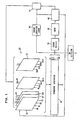
- Fig. 1 shows a memory 32 for storing 144-bit code words or quadwords on 36 cards 10 each containing four bit positions of the code word, where 128 of the bit positions are data bits and the remainder are ECC (error correction code) check bits of a double error correction/triple error detection (DEC/TED) code.
- ECC error correction code
- DEC/TED double error correction/triple error detection
- An X-Y coordinate address of 16 bits is supplied to all of the chips 12 on the cards 10. This address is supplied to a word decoder 11 and a bit decoder 13 to select a single storage cell in each of the arrays 12. Thus, as a result of a combination of a row select address and an X-Y coordinate address a single bit in each of the 144 columns shown in Fig. 1 is selected.
- This memory is a paging store, that is, data is read out of this store in pages of 256 code words each.
- the pages are interleaved among the arrays 12 in each column, with bits of 16 code words of a page in a given array 12.
- Each code word in a page has the same Y address, 1 of 16 different X addresses and of course any code word of a page may have 1 of 16 different chip row addresses.
- Fig. 3 shows three of the arrays 12a, 12b and 12p for bits in the first bit position of code words.
- the numbers on the bits correspond to page, and word position.
- the left hand bit in the top most row of array 12a is numbered 1-1 since it is in the first word of the first page.
- the next bit position in that row is numbered 1-17 since it is in the 17th word of the first page and so on until the last or right hand bit which is numbered 16-241 to indicate it is in the 241st word of the sixteenth page.
- the second row of the array contains the storage cells for the first bit position of words 1, 17, 33...241 for the 17th to 32nd pages
- the third line contains the storage cells for the first bit position of words 1, 17, 33...241 of the 33rd to 48th pages and so on until the 4096th page.
- Cells for bit positions of words 2, 18, 34...242 for pages 1 to 4096 are contained on the second chip 12b and cells for the bit positions of words 3, 19, 35...243 of pages 1 to 4096 are contained on the third chip (not shown) and so on, so that all bits in the first bit position of all code words for the first 4096 pages are contained on the top 16 chips 12a-p of the first column.
- Fig. 4 shows the effect that different types of failure categories have on this memory.
- the first column describes the type of failure.
- the second column tells the number of pages affected by the type of failure listed alongside it in the first column.
- the third column tells how many words per page will be affected by the failures, while the fourth and fifth columns contain the word and page address patterns of the faults.
- the first seven bits R0-R6 of the substitution address are fed into a compare circuit 22 where bit R0 operates as a compare circuit enable signal and bits R1 to R6 are compared with the chip row select address. If they match, a compare signal C is generated enabling the appropriate spare 16 so that it can be accessed through the data gating circuitry 18 in place of a bad chip.
- the output of the compare circuit 22 is also used to enable the one of two decoder circuits 19 which receives the other three substitution address bits R7-R9 fed into the particular shift register 20.
- the decode circuit selects one of the four bit or column positions B i to B i+3 for substituting the spare array 16 for the array 12 in that column position only when the spare 16 is activated by an enabling output from the compare circuit.
- the output of the decoder 19 is fed to the data gating select circuit 18 controlling the output of the particular bit position.
- each bit position B i to B i+3 on the card 10 one output line from each of the decoders 19 is fed into an OR gate 23. So long as the given decoder output of both decoders 19 is not up, the complemented output of OR gate 23 activates an AND gate 24 to pass data to and from the chips 12 along the bit line B i . When either decoder output in that bit position comes up the AND gate 24 becomes deactivated and an AND gate 26 is activated by the true of that decoder's output substituting one of the spares 16 for the disabled chip 12.
- the substitution of array chips 16 for a chip 12 is controlled by a count of the non-zero syndromes generated by the ECC logic 30 shown in Fig. 1.
- the ECC logic 30 receives a 144-bit code word from the memory 32 and generates error syndrome bits S1-S16 by comparing stored check bits with ECC generated check bits.
- a non-zero detector 36 generates an output each time the syndrome bits are not all zero and feeds this output to a counter 38. This counter is automatically reset to zero at regular time intervals.
- This counter 38 counts the outputs of the non-zero detector 36 between reset times and if the count exceeds a threshold count one or more times during this interval, then the counter provides a signal to the chip kill testing apparatus 40 and resets itself to zero.
- the testing apparatus 40 then tests the memory for a bad chip. If a completely bad chip 12 is detected, its address is sent by spare replacement logic control function 42 in the memory controller or maintenance console into one of the registers 20 of the card 10 on which the bad chip 12 is mounted to substitute a spare chip 16 for the failed chip 12.
- the system determines the address of the bad chip from the syndrome bits S1 to S16 of the code words or by other code words in the error pattern of Fig. 4 which update the counter.
- test does not turn up a completely bad chip it will not cause the substitution. Instead, it allows the faulty but still viable chip 12 to remain in the memory until the computer system containing the memory goes into diagnostic mode for some other reason. Then a complete diagnostic analysis of the whole memory system is performed and the locations of bad bit lines or word lines are detected and the spares are used to substitute for faulty chips, giving the highest priority for chip-kills causing UEs (uncorrectable errors), followed by island-kills and line-kills respectively. Because of the periodic resetting of the counter 38 it is unlikely that chips containing individual cell fails or line fails will invoke the test procedure because the count in the counter will never reach the count of the threshold level before the counter is cleared. Therefore, only when there is a chip with a chip-kill or island-kill type of fault, the test procedure is performed.
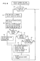
- the page and word address P j A i of the addressed word containg the bad bit is stored and the bit location is generated by the bad bit locator 44 and also stored, in step 45.
- the next step 46 is to test the memory for killed chips. This is done by generating syndromes for words P j A (j+16) and P (j+16) A i . As can be seen from Fig.
- bit locations of words P j A (i+16) and P (j+16) A i are located on the same chip adjacent to the failed bit in P j A i on a common bit or word line with the failed bit.
- the assumption being made in the test is that if two bits on the same line are bad the line is bad and if both the tested word line and bit line are bad the chip is all bad.
- the testing is done by placing test words into the memory and generating the syndromes from those test words.
- step 56 of Fig. 6 the chip is replaced on the fly and the syndrome counter 38 is reset in step 60. If a chipkill is not found, the counter continues to count and automatically resets at a regular time interval. If the threshold is not exceeded again, normal operation is continued without substitution. If the threshold is exceeded in step 62, the page Pj is deallocated and normal operation is continued. The page is also deallocated when an uncorrectable error (UE) is detected by the ECC apparatus and normal operation is resumed. As explained previously, the next time the machine goes into diagnostic mode, all or some spare chips can be assigned in such a way so that UEs and correctable errors in the memory BSM are minimized.
- UE uncorrectable error
- This embodiment is of a paging store.
- EP Application No. of same priority date herewith and entitled "Reconfigurable Memory Using Both Address Permutation and Spare Memory Elements” the invention is not limited to backing stores with certain modifications.
- This sparing technique can be used in combination with address permutation apparatus in small main stores, or in combination with double complement apparatus using the same testing algorithm.
- the testing algorithm is a function of memory organization. Before the testing techniques described herein can be used, the location of bits indicating chip kills or bits indicating word and bit line failures must be identified in the memory under consideration.
- FIG. 7 Another memory using the same testing algorithm is shown in Fig. 7.
- the placement of the two spares 16 can be made into any one of the 144 chips on the card where each chip contains one bit B i of the code word.
- Such card organization is selected for obtaining high data rate from the BSM.
- a substitution is made when either select bit S1 or S2 is non-zero, activating one of the decoders.
- the bit position replacement address bits R1 to R8 in the particular shift register specifies which array is to be replaced.
- the decoders, data gating and shift registers operate in the manner described in connection with the previously described embodiment to accomplish the substitution.
- FIG. 8 A third embodiment of card design is shown in Fig. 8 where multibit chips of 256K bit each are organized as 64 x 2 chip array. This also uses one or two spare arrays per card.
- the ECC code with this embodiment is single error correct/single package detect. Upon the detection of a 2-4 bit package error the spare is substituted for defective arrays, while single bit errors in BSM are corrected by the single bit error correction capability of the code.
- the unit of replacement can also be multi-chip array modules on a card or complete array cards in a BSM. Such card and module replacements may be necessary in some cases to overcome a support logic fail. Also, the designer can choose to make replacements offline after each memory diagnostic step for simplification.
Landscapes
- Engineering & Computer Science (AREA)
- Theoretical Computer Science (AREA)
- Quality & Reliability (AREA)
- Physics & Mathematics (AREA)
- General Engineering & Computer Science (AREA)
- General Physics & Mathematics (AREA)
- For Increasing The Reliability Of Semiconductor Memories (AREA)
- Techniques For Improving Reliability Of Storages (AREA)
Claims (9)
- Système informatique comportant une mémoire (32) protégée par un agencement de vérification d'erreur (30,36,44), dans laquelle des données sont stockées dans des mots de code à positions binaires multiples avec des positions de bit différentes sur des matrices différentes (12), avec des moyens de substitution de matrice de réserve (16,18,20,42) pour substituer une matrice de réserve (16) à une matrice défectueuse (12), caractérisé par :
des moyens de comptage (38) pour compter le nombre d'apparitions de signaux de syndrome non zéro fournis par un générateur de syndrome (30) dudit agencement de vérification d'erreur (36), lesdits moyens de comptage étant remis à zéro à intervalles de temps réguliers ou lorsqu'ils atteignent un compte de seuil ;
des moyens d'essai (40) pour essayer la mémoire en ce qui concerne des matrices défectueuses, au moyen dudit agencement de vérification d'erreur, lorsque le compte dans le compteur dépasse ce compte de seuil ; et
des moyens logiques de remplacement de matrice de réserve (42) commandés par lesdits moyens d'essai et par des moyens logiques de localisation d'erreur (44) du dit agencement de vérification d'erreur. - Système suivant la revendication 1,dans lequel ledit agencement de vérification d'erreur est un système de détection et de correction d'erreur, et
ledit compte de seuil est supérieur au compte probablement engendré par des défaillances de cellule unique dans ces matrices pendant cet intervalle de temps mais il est dépassé par des défaillances multiples du type à rangée entière et colonne entière dans une matrice unique et il détecte donc ce type de défaillances. - Système suivant la revendication 2, dans lequel lesdits moyens d'essai (40) recherchent les défaillances multiples du type rangée et colonne, et lesdits moyens logiques de remplacement de réserve (42) effectuent cette substitution seulement lorsque lesdits moyens d'essai détectent une défaillance multiple de rangée et de colonne.
- Système suivant la revendication 1, dans lequel les positions de bit d'un mot de code sont contenues dans une pluralité de cartes de mémoire (10), contenant chacune une pluralité de matrices, et dans lequel chaque carte comprend un petit nombre de matrices de réserve (16) et, pour chaquedite matrice de réserve, il est prévu un registre séparé (20), pour stocker une adresse de substitution de matrice, et un circuit de comparaison (22) pour comparer ladite adresse de substitution stockée avec la partie correspondante de l'adresse de matrice existante et pour émettre un signal d'activation de matrice de réserve (C) lorsque les adresses de matrice comparées concordent.
- Système suivant la revendication 4, dans lequel chaque carte (10) comprend en outre un circuit décodeur (19) pour chaque dite matrice de réserve (16), le dit décodeur étant activé par ledit signal d'activation de matrice de réserve (C) venant dudit circuit de comparaison (22) pour décoder un certain nombre de bits d'adresse de matrice de poids faible (R7,R8) également stockés dans ledit registre (20) et pour sélectionner une d'une pluralité de portes (18) d'entrée/sortie de bit de données prévues pour substituer des bits de données, vers/à partir de ladite matrice de réserve (16), aux bits de données vers/à partir de ladite matrice de mémoire (12) qui est à remplacer.
- Système suivant l'une quelconque des revendications précédentes, comprenant des moyens (42) pour substituer les matrices de réserve à des matrices comportant au moins une défaillance de rangée ou colonne unique lorsque lesdites matrices ne sont pas utilisées pour remplacer une matrice défectueuse.
- Dans un système informatique comprenant une mémoire protégée par un agencement de vérification d'erreur,dans laquelle des données sont stockées en mots de code multibits avec des positions de bit différentes sur des matrices différentes , la méthode comprenant :
le comptage, pendant des intervalles de temps périodiques du temps de fonctionnement de la mémoire, du nombre d'apparitions d'erreurs corrigibles détectées par l'agencement de vérification d'erreur ;
l'essai (52-56,45,46) de la mémoire pour rechercher les matrices défectueuses, au moyen des signaux de syndrome fournis par ledit agencement de vérification d'erreur (30,36,44), lorsque le compte desdites apparitions dépasse un nombre prédéterminé supérieur aux apparitions qui sont probablement engendrées par des défaillances de bit unique sans relation ; et
la substitution (60,66) d'une matrice de réserve à une matrice dont les essais indiquent qu'elle contient des défaillances autres que des défaillances de bit unique sans relation, les matrices contenant des bits bloqués sans relation étant laissées dans la mémoire. - Méthode suivant la revendication 7, dans laquelle le remplacement des matrices classées comme ayant des défaillances de puce est effectué (60) au vol à la fin de l'essai, mais les matrices classées comme ayant des défaillances de ligne de bit ou des défaillances de ligne de mot sont remplacées (66) plus tard lorque la mémoire passe en mode de diagnostic suivant, sur la base des bits disponibles des matrices de réserve à ce moment.
- Méthode suivant la revendication 7, dans laquelle ledit comptage est effectué en différé, pendant le diagnostic de la mémoire, pour détecter le type de défaut de mémoire.
Applications Claiming Priority (2)
| Application Number | Priority Date | Filing Date | Title |
|---|---|---|---|
| US06/528,769 US4584681A (en) | 1983-09-02 | 1983-09-02 | Memory correction scheme using spare arrays |
| US528769 | 1983-09-02 |
Publications (3)
| Publication Number | Publication Date |
|---|---|
| EP0136443A2 EP0136443A2 (fr) | 1985-04-10 |
| EP0136443A3 EP0136443A3 (en) | 1987-09-02 |
| EP0136443B1 true EP0136443B1 (fr) | 1991-05-29 |
Family
ID=24107112
Family Applications (1)
| Application Number | Title | Priority Date | Filing Date |
|---|---|---|---|
| EP84108714A Expired EP0136443B1 (fr) | 1983-09-02 | 1984-07-24 | Schéma de correction de mémoire utilisant des matrices de réserve |
Country Status (4)
| Country | Link |
|---|---|
| US (1) | US4584681A (fr) |
| EP (1) | EP0136443B1 (fr) |
| JP (1) | JPS6072048A (fr) |
| DE (1) | DE3484636D1 (fr) |
Cited By (1)
| Publication number | Priority date | Publication date | Assignee | Title |
|---|---|---|---|---|
| DE112019007688B4 (de) * | 2019-09-05 | 2025-07-24 | Microchip Technology Inc. | Fehlertolerantes Speicher-Array und Verfahren zum Durchführen einer Fehlerkorrektur in einem Speicher-Array |
Families Citing this family (65)
| Publication number | Priority date | Publication date | Assignee | Title |
|---|---|---|---|---|
| JPS61264599A (ja) * | 1985-05-16 | 1986-11-22 | Fujitsu Ltd | 半導体記憶装置 |
| JPH0194599A (ja) * | 1987-10-05 | 1989-04-13 | Mitsubishi Electric Corp | 半導体記憶装置 |
| US5268319A (en) * | 1988-06-08 | 1993-12-07 | Eliyahou Harari | Highly compact EPROM and flash EEPROM devices |
| JPH0793037B2 (ja) * | 1988-11-21 | 1995-10-09 | 三菱電機株式会社 | 半導体記憶装置 |
| US4964129A (en) * | 1988-12-21 | 1990-10-16 | Bull Hn Information Systems Inc. | Memory controller with error logging |
| FR2643993B1 (fr) * | 1989-03-03 | 1991-05-17 | Bull Sa | Procede pour remplacer des modules memoire dans un systeme informatique et systeme informatique pour la mise en oeuvre du procede |
| EP0675502B1 (fr) | 1989-04-13 | 2005-05-25 | SanDisk Corporation | Système EEPROM avec effacement en bloc contenant des puces multiples |
| US7190617B1 (en) * | 1989-04-13 | 2007-03-13 | Sandisk Corporation | Flash EEprom system |
| JPH0760413B2 (ja) * | 1989-05-12 | 1995-06-28 | インターナショナル・ビジネス・マシーンズ・コーポレーション | メモリ・システム |
| US5247618A (en) * | 1989-06-30 | 1993-09-21 | Digital Equipment Corporation | Transferring data in a digital data processing system |
| EP0405859B1 (fr) * | 1989-06-30 | 1997-09-17 | Digital Equipment Corporation | Procédé et dispositif pour gérer un système de mémoire de recopie |
| US5239637A (en) * | 1989-06-30 | 1993-08-24 | Digital Equipment Corporation | Digital data management system for maintaining consistency of data in a shadow set |
| US5210865A (en) * | 1989-06-30 | 1993-05-11 | Digital Equipment Corporation | Transferring data between storage media while maintaining host processor access for I/O operations |
| AU5930390A (en) * | 1989-07-06 | 1991-02-06 | Mv Limited | A fault tolerant data storage system |
| JPH0387000A (ja) * | 1989-08-30 | 1991-04-11 | Mitsubishi Electric Corp | 半導体記憶装置 |
| JP2617026B2 (ja) * | 1989-12-22 | 1997-06-04 | インターナショナル・ビジネス・マシーンズ・コーポレーション | 障害余裕性メモリ・システム |
| JPH0498342A (ja) * | 1990-08-09 | 1992-03-31 | Mitsubishi Electric Corp | 半導体記憶装置 |
| GB9023867D0 (en) * | 1990-11-02 | 1990-12-12 | Mv Ltd | Improvements relating to a fault tolerant storage system |
| JP2796590B2 (ja) * | 1991-08-07 | 1998-09-10 | 三菱電機株式会社 | メモリ装置及びそれを使用したデータ処理装置 |
| KR0121800B1 (ko) * | 1992-05-08 | 1997-11-22 | 사또오 후미오 | 메모리 카드장치 |
| US5321697A (en) * | 1992-05-28 | 1994-06-14 | Cray Research, Inc. | Solid state storage device |
| GB9305801D0 (en) * | 1993-03-19 | 1993-05-05 | Deans Alexander R | Semiconductor memory system |
| DE4329012A1 (de) * | 1993-08-28 | 1995-03-02 | Sel Alcatel Ag | Verfahren und Vorrichtung zur Fehlerprüfung und zur Fehlerkorrektur in Speicherbausteinen |
| US5502333A (en) * | 1994-03-30 | 1996-03-26 | International Business Machines Corporation | Semiconductor stack structures and fabrication/sparing methods utilizing programmable spare circuit |
| DE19540915A1 (de) * | 1994-11-10 | 1996-05-15 | Raymond Engineering | Redundante Anordnung von Festkörper-Speicherbausteinen |
| GB2292236A (en) * | 1995-04-04 | 1996-02-14 | Memory Corp Plc | Improved partial memory engine |
| KR0182939B1 (ko) * | 1995-06-28 | 1999-04-15 | 김광호 | 특정 기록포멧을 갖는 아이씨 카드 메모리 및 그로부터의 디지탈음성 기록 및 재생방법 |
| US5686843A (en) * | 1995-06-30 | 1997-11-11 | International Business Machines Corporation | Methods and apparatus for burn-in stressing and simultaneous testing of semiconductor device chips in a multichip module |
| GB2312974A (en) * | 1996-05-10 | 1997-11-12 | Memory Corp Plc | Memory replacement |
| US5764650A (en) * | 1996-08-02 | 1998-06-09 | Micron Technology, Inc. | Intelligent binning for electrically repairable semiconductor chips |
| US6138256A (en) | 1998-03-27 | 2000-10-24 | Micron Technology, Inc. | Intelligent binning for electrically repairable semiconductor chips |
| US5883904A (en) * | 1997-04-14 | 1999-03-16 | International Business Machines Corporation | Method for recoverability via redundant cache arrays |
| US6295591B1 (en) * | 1999-03-30 | 2001-09-25 | International Business Machines Corporation | Method of upgrading and/or servicing memory without interrupting the operation of the system |
| US6708248B1 (en) * | 1999-07-23 | 2004-03-16 | Rambus Inc. | Memory system with channel multiplexing of multiple memory devices |
| US6370668B1 (en) * | 1999-07-23 | 2002-04-09 | Rambus Inc | High speed memory system capable of selectively operating in non-chip-kill and chip-kill modes |
| US20020196687A1 (en) * | 2001-06-08 | 2002-12-26 | Sauvageau Anthony J. | Methods and apparatus for analyzing and repairing memory |
| US6941493B2 (en) * | 2002-02-27 | 2005-09-06 | Sun Microsystems, Inc. | Memory subsystem including an error detection mechanism for address and control signals |
| US20030163769A1 (en) * | 2002-02-27 | 2003-08-28 | Sun Microsystems, Inc. | Memory module including an error detection mechanism for address and control signals |
| US6973613B2 (en) * | 2002-06-28 | 2005-12-06 | Sun Microsystems, Inc. | Error detection/correction code which detects and corrects component failure and which provides single bit error correction subsequent to component failure |
| US6996766B2 (en) * | 2002-06-28 | 2006-02-07 | Sun Microsystems, Inc. | Error detection/correction code which detects and corrects a first failing component and optionally a second failing component |
| US6976194B2 (en) * | 2002-06-28 | 2005-12-13 | Sun Microsystems, Inc. | Memory/Transmission medium failure handling controller and method |
| US6996686B2 (en) * | 2002-12-23 | 2006-02-07 | Sun Microsystems, Inc. | Memory subsystem including memory modules having multiple banks |
| US7779285B2 (en) * | 2003-02-18 | 2010-08-17 | Oracle America, Inc. | Memory system including independent isolated power for each memory module |
| US7530008B2 (en) | 2003-08-08 | 2009-05-05 | Sun Microsystems, Inc. | Scalable-chip-correct ECC scheme |
| US7493534B2 (en) * | 2003-08-29 | 2009-02-17 | Hewlett-Packard Development Company, L.P. | Memory error ranking |
| US7188296B1 (en) | 2003-10-30 | 2007-03-06 | Sun Microsystems, Inc. | ECC for component failures using Galois fields |
| US7484065B2 (en) | 2004-04-20 | 2009-01-27 | Hewlett-Packard Development Company, L.P. | Selective memory allocation |
| US7555677B1 (en) * | 2005-04-22 | 2009-06-30 | Sun Microsystems, Inc. | System and method for diagnostic test innovation |
| US7360132B1 (en) * | 2005-05-19 | 2008-04-15 | Sun Microsystems, Inc. | System and method for memory chip kill |
| US20080077840A1 (en) * | 2006-09-27 | 2008-03-27 | Mark Shaw | Memory system and method for storing and correcting data |
| US7512772B2 (en) * | 2007-01-08 | 2009-03-31 | International Business Machines Corporation | Soft error handling in microprocessors |
| US8473791B2 (en) * | 2007-04-30 | 2013-06-25 | Hewlett-Packard Development Company, L.P. | Redundant memory to mask DRAM failures |
| JP2008217811A (ja) * | 2008-04-03 | 2008-09-18 | Hitachi Ltd | 不揮発メモリを使用したディスク制御装置 |
| US8555141B2 (en) * | 2009-06-04 | 2013-10-08 | Lsi Corporation | Flash memory organization |
| US8560924B2 (en) * | 2010-01-05 | 2013-10-15 | International Business Machines Corporation | Register file soft error recovery |
| US9043661B2 (en) | 2012-05-30 | 2015-05-26 | Micron Technology, Inc. | Memories and methods for performing column repair |
| US9459956B2 (en) | 2013-07-19 | 2016-10-04 | Seagate Technology Llc | Data decoder with trapping set flip bit mapper |
| US9317361B2 (en) | 2013-11-27 | 2016-04-19 | Seagate Technology Llc | Bit-line defect detection using unsatisfied parity code checks |
| US9891864B2 (en) | 2016-01-19 | 2018-02-13 | Micron Technology, Inc. | Non-volatile memory module architecture to support memory error correction |
| US10120749B2 (en) | 2016-09-30 | 2018-11-06 | Intel Corporation | Extended application of error checking and correction code in memory |
| JP6841698B2 (ja) * | 2017-03-21 | 2021-03-10 | ルネサスエレクトロニクス株式会社 | 半導体装置 |
| US10643734B2 (en) * | 2018-06-27 | 2020-05-05 | Micron Technology, Inc. | System and method for counting fail bit and reading out the same |
| US10990472B2 (en) | 2018-07-24 | 2021-04-27 | Micron Technology, Inc. | Spare substitution in memory system |
| KR20210147131A (ko) | 2020-05-27 | 2021-12-07 | 삼성전자주식회사 | 반도체 메모리 모듈을 액세스하는 방법 |
| KR20220060156A (ko) | 2020-11-04 | 2022-05-11 | 삼성전자주식회사 | 반도체 메모리 장치 및 반도체 메모리 장치의 동작 방법 |
Family Cites Families (19)
| Publication number | Priority date | Publication date | Assignee | Title |
|---|---|---|---|---|
| DE1963895C3 (de) * | 1969-06-21 | 1973-11-29 | Licentia Patent-Verwaltungs-Gmbh, 6000 Frankfurt | Datenspeicher und Datenspeicher anste'uerschaltung |
| SE358755B (fr) * | 1972-06-09 | 1973-08-06 | Ericsson Telefon Ab L M | |
| US3906200A (en) * | 1974-07-05 | 1975-09-16 | Sperry Rand Corp | Error logging in semiconductor storage units |
| US3999051A (en) * | 1974-07-05 | 1976-12-21 | Sperry Rand Corporation | Error logging in semiconductor storage units |
| US3917933A (en) * | 1974-12-17 | 1975-11-04 | Sperry Rand Corp | Error logging in LSI memory storage units using FIFO memory of LSI shift registers |
| US4066880A (en) * | 1976-03-30 | 1978-01-03 | Engineered Systems, Inc. | System for pretesting electronic memory locations and automatically identifying faulty memory sections |
| US4093985A (en) * | 1976-11-05 | 1978-06-06 | North Electric Company | Memory sparing arrangement |
| US4209846A (en) * | 1977-12-02 | 1980-06-24 | Sperry Corporation | Memory error logger which sorts transient errors from solid errors |
| US4414665A (en) * | 1979-11-21 | 1983-11-08 | Nippon Telegraph & Telephone Public Corp. | Semiconductor memory device test apparatus |
| JPS5694598A (en) * | 1979-12-27 | 1981-07-31 | Fujitsu Ltd | Memory error correction control system |
| US4371930A (en) * | 1980-06-03 | 1983-02-01 | Burroughs Corporation | Apparatus for detecting, correcting and logging single bit memory read errors |
| JPS5717896A (en) * | 1980-07-07 | 1982-01-29 | Tokyo Shibaura Electric Co | Spent fuel storing device |
| JPS6051199B2 (ja) * | 1980-11-13 | 1985-11-12 | 富士通株式会社 | 半導体装置 |
| US4422161A (en) * | 1981-10-08 | 1983-12-20 | Rca Corporation | Memory array with redundant elements |
| JPS5862900A (ja) * | 1981-10-08 | 1983-04-14 | Nec Corp | メモリの単一ビツトエラ−処理方式 |
| WO1983002164A1 (fr) * | 1981-12-17 | 1983-06-23 | Ryan, Philip, Meade | Dispositif de localisation a haute vitesse de defauts dans les memoires etendues |
| US4456995A (en) * | 1981-12-18 | 1984-06-26 | International Business Machines Corporation | Apparatus for high speed fault mapping of large memories |
| US4450559A (en) * | 1981-12-24 | 1984-05-22 | International Business Machines Corporation | Memory system with selective assignment of spare locations |
| US4459685A (en) * | 1982-03-03 | 1984-07-10 | Inmos Corporation | Redundancy system for high speed, wide-word semiconductor memories |
-
1983
- 1983-09-02 US US06/528,769 patent/US4584681A/en not_active Expired - Lifetime
-
1984
- 1984-07-24 EP EP84108714A patent/EP0136443B1/fr not_active Expired
- 1984-07-24 DE DE8484108714T patent/DE3484636D1/de not_active Expired - Lifetime
- 1984-08-31 JP JP59180910A patent/JPS6072048A/ja active Pending
Cited By (1)
| Publication number | Priority date | Publication date | Assignee | Title |
|---|---|---|---|---|
| DE112019007688B4 (de) * | 2019-09-05 | 2025-07-24 | Microchip Technology Inc. | Fehlertolerantes Speicher-Array und Verfahren zum Durchführen einer Fehlerkorrektur in einem Speicher-Array |
Also Published As
| Publication number | Publication date |
|---|---|
| JPS6072048A (ja) | 1985-04-24 |
| DE3484636D1 (de) | 1991-07-04 |
| EP0136443A3 (en) | 1987-09-02 |
| US4584681A (en) | 1986-04-22 |
| EP0136443A2 (fr) | 1985-04-10 |
Similar Documents
| Publication | Publication Date | Title |
|---|---|---|
| EP0136443B1 (fr) | Schéma de correction de mémoire utilisant des matrices de réserve | |
| EP0105402B1 (fr) | Appareil de permutation d'adresses de mémoire | |
| KR100337218B1 (ko) | 스크루빙 및 스페어링을 향상시킨 컴퓨터 램 메모리 시스템 | |
| US5233614A (en) | Fault mapping apparatus for memory | |
| US5659678A (en) | Fault tolerant memory | |
| US4380066A (en) | Defect tolerant memory | |
| US5267242A (en) | Method and apparatus for substituting spare memory chip for malfunctioning memory chip with scrubbing | |
| US20060265636A1 (en) | Optimized testing of on-chip error correction circuit | |
| US5299202A (en) | Method and apparatus for configuration and testing of large fault-tolerant memories | |
| EP0281740B1 (fr) | Mémoires et leur essai | |
| US5109360A (en) | Row/column address interchange for a fault-tolerant memory system | |
| CA1179060A (fr) | Memoire a semiconduteur | |
| US6457067B1 (en) | System and method for detecting faults in storage device addressing logic | |
| US4485471A (en) | Method of memory reconfiguration for fault tolerant memory | |
| US4562576A (en) | Data storage apparatus | |
| US4461001A (en) | Deterministic permutation algorithm | |
| US7490274B2 (en) | Method and apparatus for masking known fails during memory tests readouts | |
| KR100609343B1 (ko) | 컴퓨터 메모리 시스템에서의 멀티-비트 에러 보호를 위한시스템 및 방법 | |
| US8321726B2 (en) | Repairing memory arrays | |
| US6560731B2 (en) | Method for checking the functioning of memory cells of an integrated semiconductor memory | |
| US20240265987A1 (en) | Memory repair circuit, a memory repair method, and a memory device | |
| Szygenda et al. | Coding techniques for failure recovery in a distributive modular memory organization | |
| Kim et al. | Stay Alive, Don't Give Up: DUE and SDC Reduction with Memory Repair | |
| JPH01288947A (ja) | バッファメモリ障害処理方式 |
Legal Events
| Date | Code | Title | Description |
|---|---|---|---|
| PUAI | Public reference made under article 153(3) epc to a published international application that has entered the european phase |
Free format text: ORIGINAL CODE: 0009012 |
|
| 17P | Request for examination filed |
Effective date: 19841123 |
|
| AK | Designated contracting states |
Designated state(s): DE FR GB |
|
| PUAL | Search report despatched |
Free format text: ORIGINAL CODE: 0009013 |
|
| AK | Designated contracting states |
Kind code of ref document: A3 Designated state(s): DE FR GB |
|
| 17Q | First examination report despatched |
Effective date: 19890519 |
|
| GRAA | (expected) grant |
Free format text: ORIGINAL CODE: 0009210 |
|
| AK | Designated contracting states |
Kind code of ref document: B1 Designated state(s): DE FR GB |
|
| REF | Corresponds to: |
Ref document number: 3484636 Country of ref document: DE Date of ref document: 19910704 |
|
| ET | Fr: translation filed | ||
| PLBE | No opposition filed within time limit |
Free format text: ORIGINAL CODE: 0009261 |
|
| STAA | Information on the status of an ep patent application or granted ep patent |
Free format text: STATUS: NO OPPOSITION FILED WITHIN TIME LIMIT |
|
| 26N | No opposition filed | ||
| PGFP | Annual fee paid to national office [announced via postgrant information from national office to epo] |
Ref country code: GB Payment date: 19950622 Year of fee payment: 12 |
|
| PGFP | Annual fee paid to national office [announced via postgrant information from national office to epo] |
Ref country code: FR Payment date: 19950704 Year of fee payment: 12 |
|
| PGFP | Annual fee paid to national office [announced via postgrant information from national office to epo] |
Ref country code: DE Payment date: 19950720 Year of fee payment: 12 |
|
| PG25 | Lapsed in a contracting state [announced via postgrant information from national office to epo] |
Ref country code: GB Effective date: 19960724 |
|
| GBPC | Gb: european patent ceased through non-payment of renewal fee |
Effective date: 19960724 |
|
| PG25 | Lapsed in a contracting state [announced via postgrant information from national office to epo] |
Ref country code: FR Effective date: 19970328 |
|
| PG25 | Lapsed in a contracting state [announced via postgrant information from national office to epo] |
Ref country code: DE Effective date: 19970402 |
|
| REG | Reference to a national code |
Ref country code: FR Ref legal event code: ST |