EP0136534A2 - Verfahren zur Herstellung von grossflächigen integrierten Schaltungen - Google Patents
Verfahren zur Herstellung von grossflächigen integrierten Schaltungen Download PDFInfo
- Publication number
- EP0136534A2 EP0136534A2 EP84110227A EP84110227A EP0136534A2 EP 0136534 A2 EP0136534 A2 EP 0136534A2 EP 84110227 A EP84110227 A EP 84110227A EP 84110227 A EP84110227 A EP 84110227A EP 0136534 A2 EP0136534 A2 EP 0136534A2
- Authority
- EP
- European Patent Office
- Prior art keywords
- photoresist
- film
- etchable
- orifice
- viscous liquid
- Prior art date
- Legal status (The legal status is an assumption and is not a legal conclusion. Google has not performed a legal analysis and makes no representation as to the accuracy of the status listed.)
- Granted
Links
- 238000000034 method Methods 0.000 title claims abstract description 40
- 229920002120 photoresistant polymer Polymers 0.000 claims abstract description 149
- 238000000151 deposition Methods 0.000 claims abstract description 24
- 230000005855 radiation Effects 0.000 claims abstract description 20
- 239000010408 film Substances 0.000 claims description 70
- 239000000203 mixture Substances 0.000 claims description 53
- 239000000463 material Substances 0.000 claims description 40
- 239000004065 semiconductor Substances 0.000 claims description 35
- 239000010409 thin film Substances 0.000 claims description 30
- 239000000758 substrate Substances 0.000 claims description 25
- 239000002904 solvent Substances 0.000 claims description 21
- 230000008021 deposition Effects 0.000 claims description 15
- 229920005989 resin Polymers 0.000 claims description 12
- 239000011347 resin Substances 0.000 claims description 12
- 238000010438 heat treatment Methods 0.000 claims description 10
- 239000007788 liquid Substances 0.000 claims description 10
- 238000005530 etching Methods 0.000 claims description 9
- 239000004020 conductor Substances 0.000 claims description 5
- 239000007787 solid Substances 0.000 claims description 5
- WBYWAXJHAXSJNI-UHFFFAOYSA-N cinnamic acid Chemical class OC(=O)C=CC1=CC=CC=C1 WBYWAXJHAXSJNI-UHFFFAOYSA-N 0.000 claims description 4
- SLGWESQGEUXWJQ-UHFFFAOYSA-N formaldehyde;phenol Chemical compound O=C.OC1=CC=CC=C1 SLGWESQGEUXWJQ-UHFFFAOYSA-N 0.000 claims description 3
- 229920001568 phenolic resin Polymers 0.000 claims description 3
- 239000003504 photosensitizing agent Substances 0.000 claims description 3
- ISWSIDIOOBJBQZ-UHFFFAOYSA-N Phenol Chemical compound OC1=CC=CC=C1 ISWSIDIOOBJBQZ-UHFFFAOYSA-N 0.000 claims description 2
- 150000008425 anthrones Chemical class 0.000 claims description 2
- 125000000852 azido group Chemical group *N=[N+]=[N-] 0.000 claims description 2
- 235000010290 biphenyl Nutrition 0.000 claims description 2
- 125000006267 biphenyl group Chemical group 0.000 claims description 2
- 150000004770 chalcogenides Chemical class 0.000 claims description 2
- 239000012212 insulator Substances 0.000 claims description 2
- VBEGHXKAFSLLGE-UHFFFAOYSA-N n-phenylnitramide Chemical class [O-][N+](=O)NC1=CC=CC=C1 VBEGHXKAFSLLGE-UHFFFAOYSA-N 0.000 claims description 2
- 150000002828 nitro derivatives Chemical class 0.000 claims description 2
- 150000004053 quinones Chemical class 0.000 claims description 2
- 150000003549 thiazolines Chemical class 0.000 claims description 2
- 239000012633 leachable Substances 0.000 claims 7
- 230000001464 adherent effect Effects 0.000 claims 2
- WTQZSMDDRMKJRI-UHFFFAOYSA-N 4-diazoniophenolate Chemical compound [O-]C1=CC=C([N+]#N)C=C1 WTQZSMDDRMKJRI-UHFFFAOYSA-N 0.000 claims 1
- 239000002178 crystalline material Substances 0.000 claims 1
- PYGSKMBEVAICCR-UHFFFAOYSA-N hexa-1,5-diene Chemical group C=CCCC=C PYGSKMBEVAICCR-UHFFFAOYSA-N 0.000 claims 1
- 239000010410 layer Substances 0.000 description 24
- LYCAIKOWRPUZTN-UHFFFAOYSA-N Ethylene glycol Chemical compound OCCO LYCAIKOWRPUZTN-UHFFFAOYSA-N 0.000 description 15
- 238000001125 extrusion Methods 0.000 description 11
- -1 polyvinyl cinnamates Chemical class 0.000 description 11
- 239000000243 solution Substances 0.000 description 11
- 238000011161 development Methods 0.000 description 9
- 230000008569 process Effects 0.000 description 9
- RTZKZFJDLAIYFH-UHFFFAOYSA-N Diethyl ether Chemical compound CCOCC RTZKZFJDLAIYFH-UHFFFAOYSA-N 0.000 description 8
- OKKJLVBELUTLKV-UHFFFAOYSA-N Methanol Chemical compound OC OKKJLVBELUTLKV-UHFFFAOYSA-N 0.000 description 8
- 230000015572 biosynthetic process Effects 0.000 description 7
- 229920000642 polymer Polymers 0.000 description 7
- IJGRMHOSHXDMSA-UHFFFAOYSA-N Atomic nitrogen Chemical compound N#N IJGRMHOSHXDMSA-UHFFFAOYSA-N 0.000 description 4
- KRHYYFGTRYWZRS-UHFFFAOYSA-N Fluorane Chemical compound F KRHYYFGTRYWZRS-UHFFFAOYSA-N 0.000 description 4
- GRYLNZFGIOXLOG-UHFFFAOYSA-N Nitric acid Chemical compound O[N+]([O-])=O GRYLNZFGIOXLOG-UHFFFAOYSA-N 0.000 description 4
- 239000002253 acid Substances 0.000 description 4
- 229910021417 amorphous silicon Inorganic materials 0.000 description 4
- JHIVVAPYMSGYDF-UHFFFAOYSA-N cyclohexanone Chemical compound O=C1CCCCC1 JHIVVAPYMSGYDF-UHFFFAOYSA-N 0.000 description 4
- 229910017604 nitric acid Inorganic materials 0.000 description 4
- 238000004528 spin coating Methods 0.000 description 4
- 239000007921 spray Substances 0.000 description 4
- AZQWKYJCGOJGHM-UHFFFAOYSA-N 1,4-benzoquinone Chemical compound O=C1C=CC(=O)C=C1 AZQWKYJCGOJGHM-UHFFFAOYSA-N 0.000 description 3
- YMWUJEATGCHHMB-UHFFFAOYSA-N Dichloromethane Chemical compound ClCCl YMWUJEATGCHHMB-UHFFFAOYSA-N 0.000 description 3
- 238000006243 chemical reaction Methods 0.000 description 3
- 150000008280 chlorinated hydrocarbons Chemical class 0.000 description 3
- 239000011248 coating agent Substances 0.000 description 3
- 238000000576 coating method Methods 0.000 description 3
- 150000002576 ketones Chemical class 0.000 description 3
- 229920003986 novolac Polymers 0.000 description 3
- 238000000206 photolithography Methods 0.000 description 3
- SVONRAPFKPVNKG-UHFFFAOYSA-N 2-ethoxyethyl acetate Chemical compound CCOCCOC(C)=O SVONRAPFKPVNKG-UHFFFAOYSA-N 0.000 description 2
- CSCPPACGZOOCGX-UHFFFAOYSA-N Acetone Chemical compound CC(C)=O CSCPPACGZOOCGX-UHFFFAOYSA-N 0.000 description 2
- DKPFZGUDAPQIHT-UHFFFAOYSA-N Butyl acetate Natural products CCCCOC(C)=O DKPFZGUDAPQIHT-UHFFFAOYSA-N 0.000 description 2
- YNQLUTRBYVCPMQ-UHFFFAOYSA-N Ethylbenzene Chemical compound CCC1=CC=CC=C1 YNQLUTRBYVCPMQ-UHFFFAOYSA-N 0.000 description 2
- PEDCQBHIVMGVHV-UHFFFAOYSA-N Glycerine Chemical compound OCC(O)CO PEDCQBHIVMGVHV-UHFFFAOYSA-N 0.000 description 2
- CTQNGGLPUBDAKN-UHFFFAOYSA-N O-Xylene Chemical compound CC1=CC=CC=C1C CTQNGGLPUBDAKN-UHFFFAOYSA-N 0.000 description 2
- NBIIXXVUZAFLBC-UHFFFAOYSA-N Phosphoric acid Chemical compound OP(O)(O)=O NBIIXXVUZAFLBC-UHFFFAOYSA-N 0.000 description 2
- PPBRXRYQALVLMV-UHFFFAOYSA-N Styrene Chemical compound C=CC1=CC=CC=C1 PPBRXRYQALVLMV-UHFFFAOYSA-N 0.000 description 2
- 150000004945 aromatic hydrocarbons Chemical class 0.000 description 2
- 150000001540 azides Chemical class 0.000 description 2
- 230000004888 barrier function Effects 0.000 description 2
- 229940043232 butyl acetate Drugs 0.000 description 2
- MVPPADPHJFYWMZ-UHFFFAOYSA-N chlorobenzene Chemical compound ClC1=CC=CC=C1 MVPPADPHJFYWMZ-UHFFFAOYSA-N 0.000 description 2
- 238000001035 drying Methods 0.000 description 2
- 238000001704 evaporation Methods 0.000 description 2
- 230000008020 evaporation Effects 0.000 description 2
- FUZZWVXGSFPDMH-UHFFFAOYSA-M hexanoate Chemical compound CCCCCC([O-])=O FUZZWVXGSFPDMH-UHFFFAOYSA-M 0.000 description 2
- 230000002706 hydrostatic effect Effects 0.000 description 2
- 238000005286 illumination Methods 0.000 description 2
- 238000007654 immersion Methods 0.000 description 2
- 239000003999 initiator Substances 0.000 description 2
- 230000000873 masking effect Effects 0.000 description 2
- 229910052757 nitrogen Inorganic materials 0.000 description 2
- 238000005507 spraying Methods 0.000 description 2
- 239000002344 surface layer Substances 0.000 description 2
- 150000003505 terpenes Chemical class 0.000 description 2
- 229920002554 vinyl polymer Polymers 0.000 description 2
- XLYOFNOQVPJJNP-UHFFFAOYSA-N water Chemical compound O XLYOFNOQVPJJNP-UHFFFAOYSA-N 0.000 description 2
- 239000008096 xylene Substances 0.000 description 2
- YQPDFPOALLAYGO-YDWXAUTNSA-N (1e,4e)-1,5-bis(4-azidophenyl)penta-1,4-dien-3-one Chemical compound C1=CC(N=[N+]=[N-])=CC=C1\C=C\C(=O)\C=C\C1=CC=C(N=[N+]=[N-])C=C1 YQPDFPOALLAYGO-YDWXAUTNSA-N 0.000 description 1
- RYHBNJHYFVUHQT-UHFFFAOYSA-N 1,4-Dioxane Chemical compound C1COCCO1 RYHBNJHYFVUHQT-UHFFFAOYSA-N 0.000 description 1
- HWEONUWVYWIJPF-OWOJBTEDSA-N 1-azido-4-[(e)-2-(4-azidophenyl)ethenyl]benzene Chemical compound C1=CC(N=[N+]=[N-])=CC=C1\C=C\C1=CC=C(N=[N+]=[N-])C=C1 HWEONUWVYWIJPF-OWOJBTEDSA-N 0.000 description 1
- RJKGJBPXVHTNJL-UHFFFAOYSA-N 1-nitronaphthalene Chemical compound C1=CC=C2C([N+](=O)[O-])=CC=CC2=C1 RJKGJBPXVHTNJL-UHFFFAOYSA-N 0.000 description 1
- IAHOUQOWMXVMEH-UHFFFAOYSA-N 2,4,6-trinitroaniline Chemical compound NC1=C([N+]([O-])=O)C=C([N+]([O-])=O)C=C1[N+]([O-])=O IAHOUQOWMXVMEH-UHFFFAOYSA-N 0.000 description 1
- LOCWBQIWHWIRGN-UHFFFAOYSA-N 2-chloro-4-nitroaniline Chemical compound NC1=CC=C([N+]([O-])=O)C=C1Cl LOCWBQIWHWIRGN-UHFFFAOYSA-N 0.000 description 1
- ZNQVEEAIQZEUHB-UHFFFAOYSA-N 2-ethoxyethanol Chemical compound CCOCCO ZNQVEEAIQZEUHB-UHFFFAOYSA-N 0.000 description 1
- XTTIQGSLJBWVIV-UHFFFAOYSA-N 2-methyl-4-nitroaniline Chemical compound CC1=CC([N+]([O-])=O)=CC=C1N XTTIQGSLJBWVIV-UHFFFAOYSA-N 0.000 description 1
- JQXYBDVZAUEPDL-UHFFFAOYSA-N 2-methylidene-5-phenylpent-4-enoic acid Chemical compound OC(=O)C(=C)CC=CC1=CC=CC=C1 JQXYBDVZAUEPDL-UHFFFAOYSA-N 0.000 description 1
- PYSRRFNXTXNWCD-UHFFFAOYSA-N 3-(2-phenylethenyl)furan-2,5-dione Chemical compound O=C1OC(=O)C(C=CC=2C=CC=CC=2)=C1 PYSRRFNXTXNWCD-UHFFFAOYSA-N 0.000 description 1
- JLBJTVDPSNHSKJ-UHFFFAOYSA-N 4-Methylstyrene Chemical compound CC1=CC=C(C=C)C=C1 JLBJTVDPSNHSKJ-UHFFFAOYSA-N 0.000 description 1
- BAJQRLZAPXASRD-UHFFFAOYSA-N 4-Nitrobiphenyl Chemical group C1=CC([N+](=O)[O-])=CC=C1C1=CC=CC=C1 BAJQRLZAPXASRD-UHFFFAOYSA-N 0.000 description 1
- FEIQOMCWGDNMHM-UHFFFAOYSA-N 5-phenylpenta-2,4-dienoic acid Chemical compound OC(=O)C=CC=CC1=CC=CC=C1 FEIQOMCWGDNMHM-UHFFFAOYSA-N 0.000 description 1
- RZVHIXYEVGDQDX-UHFFFAOYSA-N 9,10-anthraquinone Chemical compound C1=CC=C2C(=O)C3=CC=CC=C3C(=O)C2=C1 RZVHIXYEVGDQDX-UHFFFAOYSA-N 0.000 description 1
- 229940076442 9,10-anthraquinone Drugs 0.000 description 1
- QTBSBXVTEAMEQO-UHFFFAOYSA-M Acetate Chemical compound CC([O-])=O QTBSBXVTEAMEQO-UHFFFAOYSA-M 0.000 description 1
- VHUUQVKOLVNVRT-UHFFFAOYSA-N Ammonium hydroxide Chemical compound [NH4+].[OH-] VHUUQVKOLVNVRT-UHFFFAOYSA-N 0.000 description 1
- VEXZGXHMUGYJMC-UHFFFAOYSA-M Chloride anion Chemical compound [Cl-] VEXZGXHMUGYJMC-UHFFFAOYSA-M 0.000 description 1
- 239000004641 Diallyl-phthalate Substances 0.000 description 1
- LFQSCWFLJHTTHZ-UHFFFAOYSA-N Ethanol Chemical compound CCO LFQSCWFLJHTTHZ-UHFFFAOYSA-N 0.000 description 1
- 229920000877 Melamine resin Polymers 0.000 description 1
- XUIMIQQOPSSXEZ-UHFFFAOYSA-N Silicon Chemical compound [Si] XUIMIQQOPSSXEZ-UHFFFAOYSA-N 0.000 description 1
- 229920000147 Styrene maleic anhydride Polymers 0.000 description 1
- 238000005299 abrasion Methods 0.000 description 1
- 230000001133 acceleration Effects 0.000 description 1
- 230000009471 action Effects 0.000 description 1
- 230000004913 activation Effects 0.000 description 1
- 239000012190 activator Substances 0.000 description 1
- 239000000654 additive Substances 0.000 description 1
- 238000013019 agitation Methods 0.000 description 1
- 150000001299 aldehydes Chemical class 0.000 description 1
- 125000001931 aliphatic group Chemical group 0.000 description 1
- 239000000956 alloy Substances 0.000 description 1
- 229910045601 alloy Inorganic materials 0.000 description 1
- 229910000147 aluminium phosphate Inorganic materials 0.000 description 1
- 239000000908 ammonium hydroxide Substances 0.000 description 1
- PYKYMHQGRFAEBM-UHFFFAOYSA-N anthraquinone Natural products CCC(=O)c1c(O)c2C(=O)C3C(C=CC=C3O)C(=O)c2cc1CC(=O)OC PYKYMHQGRFAEBM-UHFFFAOYSA-N 0.000 description 1
- 239000007864 aqueous solution Substances 0.000 description 1
- 238000010420 art technique Methods 0.000 description 1
- LHMRXAIRPKSGDE-UHFFFAOYSA-N benzo[a]anthracene-7,12-dione Chemical compound C1=CC2=CC=CC=C2C2=C1C(=O)C1=CC=CC=C1C2=O LHMRXAIRPKSGDE-UHFFFAOYSA-N 0.000 description 1
- WPYMKLBDIGXBTP-UHFFFAOYSA-N benzoic acid Chemical compound OC(=O)C1=CC=CC=C1 WPYMKLBDIGXBTP-UHFFFAOYSA-N 0.000 description 1
- CHFBCXOSLARLKB-UHFFFAOYSA-N bis(4-azidophenyl)methanone Chemical compound C1=CC(N=[N+]=[N-])=CC=C1C(=O)C1=CC=C(N=[N+]=[N-])C=C1 CHFBCXOSLARLKB-UHFFFAOYSA-N 0.000 description 1
- QUDWYFHPNIMBFC-UHFFFAOYSA-N bis(prop-2-enyl) benzene-1,2-dicarboxylate Chemical compound C=CCOC(=O)C1=CC=CC=C1C(=O)OCC=C QUDWYFHPNIMBFC-UHFFFAOYSA-N 0.000 description 1
- KGBXLFKZBHKPEV-UHFFFAOYSA-N boric acid Chemical compound OB(O)O KGBXLFKZBHKPEV-UHFFFAOYSA-N 0.000 description 1
- 239000004327 boric acid Substances 0.000 description 1
- 230000001680 brushing effect Effects 0.000 description 1
- 239000008366 buffered solution Substances 0.000 description 1
- 125000002915 carbonyl group Chemical group [*:2]C([*:1])=O 0.000 description 1
- 125000003178 carboxy group Chemical group [H]OC(*)=O 0.000 description 1
- 238000012822 chemical development Methods 0.000 description 1
- 150000001805 chlorine compounds Chemical class 0.000 description 1
- 150000008422 chlorobenzenes Chemical class 0.000 description 1
- 230000000295 complement effect Effects 0.000 description 1
- 230000006835 compression Effects 0.000 description 1
- 238000007906 compression Methods 0.000 description 1
- 238000002508 contact lithography Methods 0.000 description 1
- 150000003997 cyclic ketones Chemical class 0.000 description 1
- 239000008367 deionised water Substances 0.000 description 1
- 229910021641 deionized water Inorganic materials 0.000 description 1
- 230000002939 deleterious effect Effects 0.000 description 1
- 238000005137 deposition process Methods 0.000 description 1
- 238000007598 dipping method Methods 0.000 description 1
- 230000000694 effects Effects 0.000 description 1
- 150000002148 esters Chemical class 0.000 description 1
- 235000011187 glycerol Nutrition 0.000 description 1
- 238000007756 gravure coating Methods 0.000 description 1
- 239000004922 lacquer Substances 0.000 description 1
- 238000004519 manufacturing process Methods 0.000 description 1
- JDSHMPZPIAZGSV-UHFFFAOYSA-N melamine Chemical compound NC1=NC(N)=NC(N)=N1 JDSHMPZPIAZGSV-UHFFFAOYSA-N 0.000 description 1
- QSHDDOUJBYECFT-UHFFFAOYSA-N mercury Chemical compound [Hg] QSHDDOUJBYECFT-UHFFFAOYSA-N 0.000 description 1
- 239000000178 monomer Substances 0.000 description 1
- 239000002245 particle Substances 0.000 description 1
- 230000009467 reduction Effects 0.000 description 1
- 238000007761 roller coating Methods 0.000 description 1
- 238000005096 rolling process Methods 0.000 description 1
- 229910052710 silicon Inorganic materials 0.000 description 1
- 239000010703 silicon Substances 0.000 description 1
- 239000003381 stabilizer Substances 0.000 description 1
- 239000000126 substance Substances 0.000 description 1
- 239000005720 sucrose Substances 0.000 description 1
- 238000012719 thermal polymerization Methods 0.000 description 1
- 238000005406 washing Methods 0.000 description 1
Images

Classifications
-
- G—PHYSICS
- G03—PHOTOGRAPHY; CINEMATOGRAPHY; ANALOGOUS TECHNIQUES USING WAVES OTHER THAN OPTICAL WAVES; ELECTROGRAPHY; HOLOGRAPHY
- G03F—PHOTOMECHANICAL PRODUCTION OF TEXTURED OR PATTERNED SURFACES, e.g. FOR PRINTING, FOR PROCESSING OF SEMICONDUCTOR DEVICES; MATERIALS THEREFOR; ORIGINALS THEREFOR; APPARATUS SPECIALLY ADAPTED THEREFOR
- G03F7/00—Photomechanical, e.g. photolithographic, production of textured or patterned surfaces, e.g. printing surfaces; Materials therefor, e.g. comprising photoresists; Apparatus specially adapted therefor
- G03F7/16—Coating processes; Apparatus therefor
-
- H—ELECTRICITY
- H05—ELECTRIC TECHNIQUES NOT OTHERWISE PROVIDED FOR
- H05K—PRINTED CIRCUITS; CASINGS OR CONSTRUCTIONAL DETAILS OF ELECTRIC APPARATUS; MANUFACTURE OF ASSEMBLAGES OF ELECTRICAL COMPONENTS
- H05K1/00—Printed circuits
- H05K1/02—Details
- H05K1/03—Use of materials for the substrate
- H05K1/0393—Flexible materials
-
- H—ELECTRICITY
- H05—ELECTRIC TECHNIQUES NOT OTHERWISE PROVIDED FOR
- H05K—PRINTED CIRCUITS; CASINGS OR CONSTRUCTIONAL DETAILS OF ELECTRIC APPARATUS; MANUFACTURE OF ASSEMBLAGES OF ELECTRICAL COMPONENTS
- H05K3/00—Apparatus or processes for manufacturing printed circuits
- H05K3/0091—Apparatus for coating printed circuits using liquid non-metallic coating compositions
-
- H—ELECTRICITY
- H05—ELECTRIC TECHNIQUES NOT OTHERWISE PROVIDED FOR
- H05K—PRINTED CIRCUITS; CASINGS OR CONSTRUCTIONAL DETAILS OF ELECTRIC APPARATUS; MANUFACTURE OF ASSEMBLAGES OF ELECTRICAL COMPONENTS
- H05K3/00—Apparatus or processes for manufacturing printed circuits
- H05K3/0097—Processing two or more printed circuits simultaneously, e.g. made from a common substrate, or temporarily stacked circuit boards
Definitions
- Integrated electronic circuits are typically prepared by sequentially depositing. patterned thin film layers, e.g. of connectors, contacts and conductors, atop a crystalline wafer or chip in well defined patterns. These patterned layers may be deposited by evaporation masking or photolithography.
- a physical barrier of the appropriate shape is present in close contact with the surface on which the thin film layer is to be deposited.
- the barrier intercepts defined portions of the evaporant beam. The portions intercepted are prevented from condensing on the surface. The evaporative beam condensate forms the thin film pattern on the surface.
- the thin film is already present on the surface, and the desired pattern is formed in the thin film by selective removal of portions of the film.
- the removal is accomplished by the use of light sensitive organic lacquers, i.e. photoresists.
- the photoresist is deposited atop the thin film, and the desired pattern is formed in the photoresist layer by actinic radiation.
- Development of the photoresist layer causes a significant difference in the solublity of the exposed and the unexposed regions of the photoresist layer.
- the more soluble region of the photoresist layer is removed by a suitable solvent. In this way, a portion of the underlying thin film is uncovered for the etchant and may be etched, leaving behind the desired surface pattern.
- the pattern is defined by a stencil or a mask, i.e., a photomask.
- the mask is a precision image of the pattern to be etched. It is prepared by the 200 fold to 1000 fold photographic reduction of the original art work.
- the original art work shows the pattern to be formed on the thin film at a scale readable by the unaided human eye.
- a polymeric photoresist layer is formed on the thin film to be etched.
- the photoresist layer is then exposed to actinic radiation through the photomask, e.g., by contact printing.
- Actinic radiation renders one portion of the photoresist relatively more soluble, and the other portion relatively less soluble.
- the more soluble portion of the photoresist is removed, e.g., by solublization with a suitable solvent, uncovering portions of the thin film.
- the uncovered portions of the thin film are then removed by etching, leaving behind a facsimile or reverse facsimile of the photo mask pattern.
- Prior art techniques for formation of the film of the polymeric photoresist have been developed for and are especially adapted to small, rigid elements.
- small, rigid elements are elements having no linear dimension greater then about 3 inches. They formed on or encompass a rigid, non-flexible element, for example a monocrystalline element, that is substantially free from warpage or bow.
- the prior art photoresist application techniques include spraying, dipping, spin or whirl coating, and gravure rolling. Most commonly spin coating techniques have been used. In spin coating, also known as whirl coating, a pool of photoresist composition, i.e., a pool of photoresist polymer in solvent, is formed on a surface of the element to be coated.
- the element is rotated at a speed of about 2000 to about 6000 revolutions per minute, whereby to deposit the photoresist composition substantially uniformly across the surface of the small, rigid element.
- the thickness of the photoresist deposit is a function of the viscosity and density of the photoresist composition, and the angular velocity of the element to be coated.
- Spin coating has been found to be unsuitable for both large, non-rigid, flexible elements, and for continous processes. More particularly, spin coating has been found to be unsuitable for roll to roll processes for the formation of micro circuits on flexible substrates, which substrates are of width greater than about 3 inches, which substrates are drawn from one roll through various deposition processes to a subsequent roll.
- a film of photoresist polymer in solvent may be formed, for example, by extrusion, and thereafter deposited on the surface to be coated.
- a patterned, a thin film layer of an electronic circuit is formed by the method comprising depositing photoresist material atop an etchable surface of an element of the circuit and exposing a portion of the photoresist material to actinic energy with formation of soluble and insoluble portions thereof.
- the soluble portions of the photoresist are then removed, recovering a portion of the etchable surface of the element, and the recovered portion of the etchable surface of the element is then etched to form the patterned, thin film layer.
- the photoresist is deposited by the method of forming a film of photoresist composition comprising photoresist polymer and solvent, where the film of photoresist polymer is formed separate from the etchable thin film surface of the circuit element, and thereafter depositing the film of photoresist composition on the etchable thin film surface of the circuit element.
- a film of photoresist composition is meant a substantially continuous, viscous web that is capable of maintaining its form and integrity between its discharge from the extruder and its deposition on the surface of the circuit element, as distinguished from a spray of substantially discontinuous particles.
- an electronic element or circuit for example, an intregrated circuit, having a continuous, flexible, mechanical, structural substrate supporting the circuit elements, the substrate having at least one surface dimension in excess of 3 inches.
- the flexible, mechanical structural, substrate is withdrawn from a roll of substrate material and passed through at least one stage of amorphous semiconductor material deposition means. This deposits at least one layer of amorphous semiconductor material on the flexible, structural, mechanical substrate.
- the deposit of amorphous semiconductor material has an etchable external surface.
- a film of photoresist composition is formed and deposited atop the etchable external surface.
- the film of photoresist composition is exposed to actinic radiation through a photo mask, forming soluble and insoluble portions.
- the soluble portions of the photoresist film are removed, uncovering a patterned portion of the etchable surface.
- the uncovered portions of etchable surface are then removed whereby to define a circuit element that is a facsimile or reverse facsimile of the photo mask pattern.
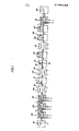
- Figure 1 shows a schematic view of the method of this invention where the flexible, mechanical substrate is withdrawn from a roll, passed through amorphous semiconductor deposition means, and thereafter passed through various chambers for photolithography, including extrusion formation of the photoresist, followed by deposition of a subsequent amorphous semiconductor layer atop the etched thin film.
- Figure 2 shows a schematic view of the formation of the photoresist film separate from the etchable surface layer and deposition of the photoresist on the etchable surface layer with draw down of the photoresist film.
- Figure 3 is an exploded, partial cut-away view of the extrusion head having an orifice therein for forming the film of photoresist material.
- the invention herein is a method of forming an electronic element, for example an integrated circuit, by the method of depositing a photoresist atop an etchable surface of a thin film of the circuit element, and exposing a portion of the photoresist to actinic radiation through a photomask whereby to form a facsimile or reverse facsimile of the photomask in the photoresist film.
- the actinic radiation forms relatively soluble and relatively insoluble portions corresponding to the photomask pattern in the photoresist film.
- the soluble portion of the photoresist is removed. This uncovers a portion of the etchable, thin film surface of the circuit element.
- the uncovered portion of the etchable thin film surface of the circuit element is then removed by etching.
- the invention is characterized in that the photoresist composition is deposited by the method comprising forming a film of photoresist composition separate from the etchable thin film surface of the circuit element and thereafter depositing the film of photoresist composition on the etchable surface of the circuit element.
- a method of forming an electronic circuit for example an integrated circuit, on a continuous, flexible, mechanical substrate,.where the mechanical substrate has at least one linear surface dimension in excess of 3 inches.
- the continuous, flexible, mechanical substrate is substantially continuously withdrawn from a roll of substrate material and passed through at least one stage of amorphous_semiconductor deposition means.
- Exemplary amorphous semiconductor deposition means are described in U.S. Patent 4,217,374 to Stanford R. Ovshinsky et al for Amorphous Semiconductor Equivalent To Crystalline Semiconductors, and U.S. Patent 4,226,898 to Stanford R.
- amorphous semiconductor material on the flexible, mechanical substrate.
- the deposit of amorphous semiconductor material has an etchable external surface, in which it is desired to etch a pattern, e.g., to define, connect, or isolate elements.
- a film comprising photoresist composition is formed separate from the etchable external surface of the amorphous semiconductor material and is thereafter deposited atop the etchable external surface.
- a photomask is placed between a source of actinic radiation and the deposited, photoresist film, and the photoresist film is exposed to actinic radiation.
- regions of relatively high solubility and relatively low solubility to form in the photoresist film.
- the regions of high solubility are removed, uncovering a pattern corresponding to the photomask or the reverse therof in the etchable surface of the amorphous semiconductor material, and overlaying the other portions of the amorphous semiconductor material.
- the uncovered portions of the etchable surface of the amorphous semiconductor material are removed by chemical etchants, forming a pattern corresponding to the photomask or the reverse thereof in the amorphous semiconductor material.
- the photoresist composition is passed through an orifice to form a film thereof and the thusly formed film of photoresist composition is thereafter deposited on the etchable surface of the circuit element.
- the orifice is an elongate horizontal orifice and the circuit element to be coated moves linearly past the orifice.
- the linear velocity of the element intended to be coated is greater then the linear velocity of the photoresist composition issuing through the orifice whereby photoresist composition film is drawn down between the orifice and the etchable surface. That is, the photoresist film is forced through the orifice at a relatively large thickness, i.e., the thickness of the orifice, and the higher linear velocity of the element to be coated thins and stretches the film of photoresist composition to form a deposited film of lesser thickness.
- the photoresist may be a negative photoresist, rendered less soluble by illumination whereby to yield a complementary or negative facsimile of the photomask.
- the photoresist is a positive photoresist which is rendered more soluble by illumination whereby to yield a positive facsimile of the photomask.
- Negative photoresists are those in which the illuminated area is rendered insoluble relative to the unexposed or masked areas of the photoresist.
- Negative photoresist resins are polymers having unsaturation, and are further polymerized by actinic radiation.
- the resin itself need not be photosensitive, but it must be capable of being rendered insoluble through reaction with a sensitizer.
- the sensitizer is capable of activation by actinic radiation.
- Exemplary negative photoresist resins include the photoactive cinnamates, such as polyvinyl cinnamates, polystyrene-cinnamyl ketones, and polyvinyl cinnamylidene acetates; diallyl phthalate prepolymer resins; and isoprenoid resins.
- the photoresist polymers are dispersed or dissolved in a solvent with a sensitizer, i.e., an activator or initiator.
- a sensitizer i.e., an activator or initiator.
- Photo sensitizers for negative photoresists are activated by near ultraviolet actinic radiation having wavelengths of 200 to 400 nanometers.
- Exemplary sensitizers for cinnamates and diallyl phthalates include azido compounds, e.g., 4,4'-azido dibenzal aldehyde; nitro compounds such as p-Nitrodiphenyl, and alpha-nitronaphthalene; nitroaniline derivatives such as 4-Nitro-2-chloroaniline, 2,4,6-Trinitroaniline, and 5-Nitro-2-amino toluene; anthrones, such as 2-Keto-3-methy1-1,3-dibenzanthrone; quinones, such as 1,2-Benzanthraquinone, Beta-Chloroanthaquinone, and 9,10-Anthraquinone; diphenyls, such as 4,4i-Tetramethyldiaminodiphenyl ketone and the analogous carbinol, and 4,4i-Tetramethyldiaminohenzophenone; and the thiazolines
- Exemplary sensitizers for isoprenoids are azides, including 4,4'-Diazidostilbene, 4,4'-Diazidobenzophenone, 2,6-Di(4i-azidobenzal)-4-methyl cyclohexanone, and 4,4'-Diazidodibenzal acetone.
- Prefered are the azides with carbonyl linkages.
- 2,6-Di-(4i-azido benzal)-4 methyl cyclohexanone because of its stability and solubility.
- various stabilizers and additives may be present to retard scum formation and thermal polymerization.
- Suitable solvents for negative photoresists include 1,4-Dioxane; aliphtic esters, for example butylacetate, and cellosolve acetate, that is, 2-ethoxy ethyl acetate; cellosolve ethers such as eteylene glycol monoethyl ether, and ethylene glycol maromethyl ether; aromatic hydrocarbons, for example xylene, and ethyl benzene.
- chlorinated hydrocarbons such as chlorobenzenes, and methyolyne chloride may be used; ketones, especially acetone and cyclical ketones such as cyclohexanone may be used.
- the photoresist material may be a positive photoresist material having a positive photoresist polymer dispersed in a suitable solvent.
- Positive photoresist polymers are low molecular weight polymers characterized by the substantial absence of unsaturation.
- a particularly preferred positive photoresist polymer is Novolak resin, a phenol terminated phenol-formaldehyde polymer.
- Other polymers may be present with the Novolak resin, and monomers thereof can even be polymerized with the phenol-terminated phenol-formaldehyde Novolak resin.
- styrene examples include styrene, methyl styrene, styrene-maleic anhydride, styrene-acrylic acid, styrene-methacrylic acid, melamine, melamine-sucrose benzoate, and the like.
- Exemplary positive photoresist sensitizers include quinone diazides, such as Benzoquinone 1,2-diazide-4-sulfochloride, Naphthaquino-1,2-diazide-5-sulfochloride, Naphthoquinone-1,2-diazide-4-sulfochloride, Naphthaquinone-2,1-diazide-4-sulfachloride, the analogous carboxy acid chlorides, and the like.
- the amount of sensitizer is from about ten weight percent to ninety weight percent, basis weight of resin, and preferably from about 25 to about 50 weight percent, basis weight of resin.
- Exemplary solvents for positive photoresists include cellosolve ethers such as ethylene glycol momoethyl ether and ethylene glycol momomethyl ether; cellosolve acetates such as ethylene glycol momoethyl ether acetate; aliphatic esters such as butylacetate; aromatic hydrocarbons such as xylene and -ethyl benzene; chlorinated hydrocarbons such as chlorobenzene and methylene chloride; and ketones, exemplified by cyclic ketones such as cyclohexanone.
- cellosolve ethers such as ethylene glycol momoethyl ether and ethylene glycol momomethyl ether
- cellosolve acetates such as ethylene glycol momoethyl ether acetate
- aliphatic esters such as butylacetate
- aromatic hydrocarbons such as xylene and -ethyl benzene
- the photoresist compositions are typically supplied in a solution of about 15 to about 45 weight percent photoresist polymer in solvent, the composition having a viscosity of from about 50 to about 125 centistokes at 25° centigrade.
- the photoresist composition is diluted to from about 2 to about 8 percent solids e.g. by adding thinner. By thinners are meant compatable solvents.
- thinners are meant compatable solvents.
- the thin, flexible film of photoresist composition is formed by forming a pool of photoresist composition in a trough of an extrusion die and imposing a hydrostatic head across the extrusion die to force the photoresist composition out of the extrusion die through an orifice.
- the film of photoresist composition is formed in close proximity to the surface to be coated, for example from about 0.002 inch to about 0.01 inch from the surface to be coated, although it may be formed further away, or even preformed.
- a thin wall of photoresist composition issues from the orifice and layers on the etchable surface of the circuit element.
- the film thickness as applied and prior to any treatment is normally greater then about 5 micron but less then about 103 microns, although thicker and thinner films may be used without deleterious effect.
- the film, as deposited, is subjected to a soft bake or a pre-bake process which is carried out with dry air.
- the soft bake or prebake may be a convective process or a resistance heating process.
- the purpose of the pre-baking is to drive off solvents. Solvents impede exposure, actinic radiation initiated chemical reactions, and development.
- the pre-bake process is typically carried out temperatures of from about 70° to about 120° centigrade for about 10 minutes to about 40 minutes, and preferably at temperatures from about 90° to about 105° centigrade at times from about 20 minutes to 30 minutes. The exact times and temperatures may be found by routine experimentation.
- the thickness of the photoresist deposit is reduced to from about 0.2 to about 2.0 micron.
- the photoresist material is exposed to actinic radiation.
- actinic radiation has wavelengths from about 200 to 500 nanometers.
- amount of actinic radiation is from about 4 to about 60 milliwatts per square centimeter for about 2 to 8 seconds and the source of the actinic radiation is a mercury vapor lamp. The exact exposure time and intensity may be found by routine experimentation.
- the photoresist is then developed to remove regions of higher relative solublity and while leaving behind regions of lower relative solublity corresponding directly or complimentary to the image of the photo mask.
- Development may be carried out by immersion, or spray. Development is carried out for times of from about 15 to about 150 seconds, and generally from about 30 to about 60 seconds. When the development is immersion development, nitrogen bubble agitation maybe used. After development the surface is rinsed, for example with deionized water.
- Spray development is particularily preferred because it allows continuous renewal of developing solution at the solution-photoresist interface. Moreover, there is a certain ablative, abrasive, brushing, or washing action of the spray which removes the more soluble fraction of the photoresist material.
- Post baking is typically carried out at temperatures from about 100° centigrade to about 200 0 centigrade, whereby to cause the less soluble portion of the photoresist, which remains after development and rinsing, to adhere more stongly to the surface of the electronic circuit element.
- etchants are dilute solutions of oxidizers, for example, nitric acid; solutions of phosphoric acid, nitric acid and hydrofluoric acid; solutions of boric acid, nitric acid and hydrofluoric acid; solutions of ammonium hydroxide in methanol with a pH of 9; buffered solutions of hydorfluoric acid; and solutions of nitric acid, hydroflouric acid and water.
- the solution is an aqueous solution, although an alcohol, such as methanol, ethylene glycol, or glycerine may be added to the acid solution to moderate the etching reaction.
- etching After etching the remaining photoresist is removed, for example by abrasion, or by hot, chlorinated hydrocarbon solutions, known in the art as degreasers. These include trichloroethylene, tetrachloroethylene, and mixtures thereof.
- Figure 1 shows a preferred exemplification of the method of this invention wherein a continuous, flexible, mechanical substrate 1 is withdrawn from a roll 101 of substrate material and passed through three amorphous semiconductor amorphous deposition chambers 103,105,107 whereby to deposit three layers of amorphous semiconductor materials.
- p-type, extrinsic semiconductor material may be applied in deposition chamber 103 followed by intrinsic amorphous silicon semiconductor in deposition chamber 105 and extrinsic, n-type amorphous silicon semiconductor in deposition chamber 107. Thereafter, a thin film or layer of conductive material may be applied atop the n-type extrinsic type semiconductor layer and subsequently have a pattern etched therein.
- the surface to be etched may be a conductor, a semiconductor, an insulator, or a material settable or switchable between said states. It may be amorphous, polycrystalline, crystalline, or switchable or settable there between, or a mixture thereof.
- the surface to be etched may be an amorphous semiconductor alloy, or a settable material having a comparatively conductive state and a comparatively non-conductive state, as a chalcogenide.
- Etching is a multi-step process which includes pre-treating the electronic circuit element, for example, by heating.
- Heating chamber 109 may contain resistance heating means 110, or conductive heating means, not shown to heat the semiconductor coated substrate a temperature of about 85°C to about 350°C for from about 10 to 30 minutes.
- the photoresist composition 11 is applied in compartment or chamber 111. It is applied as a film to the integrated circuit element, with a feed of photoresist composition through inlet 21 to an extrusion diehead 23 having an orifice 31 therein.
- the substantially continuous circuit element is drawn through the chamber 111 at a constant, linear speed without rotatory or angular velocity or acceleration components.
- the linear speed of the continuous circuit element is slightly greater than the linear speed of photoresist composition film lla from the orifice 31 in the extruder diehead 23. This results in a drawdown 116 of the photoresist composition film 11.
- the photoresist composition film 11c coated circuit element proceeds out of the coating chamber 111 to a drying chamber 113 where resistance heating elements 114 or conduction provide heating to drive off solvent which may be recovered. This step results in reducing the thickness of the photoresist film by a factor of about 5 to 400.
- the photoresist film coated continuous circuit element then proceeds to photographic chamber or compartment 115 where a photomask 116 is placed on the surface thereof and the photoresist film 11 is exposed to actinic radiation through the photomask 116, for example from light source 117. After exposure, the photoresist coated circuit element proceeds to developing and spraying chamber 119 where developer or developer and rinse are sprayed on the surface thereof. This removes regions of relatively high solubility, while allowing regions of relatively low solubility to remain substantially undisturbed thereon.
- the photoresist coated circuit element having a facsimile of the photomask thereon, and with portions of etchable surface uncovered through the photoresist, may be heated, e.g., in chamber 121, to harden the remaining photoresist. Subsequently, the photoresist coated circuit element passes to an etching chamber 123 where an etchant solution is applied thereto through nozzles 124. After etching is substansially complete the etched, photoresist coated circuit element passes to a further chamber 125 for removal of remaining photoresist material.
- the etched continous integrated circuit may be treated in a subsequent deposition chamber, for example to apply a further layer of amorphous semiconductor material or a layer of conductive material. Additionally, there may be further deposition and photoresist steps carried out and the continous circuit element is drawn up on a roller 129.
- Figure 2 shows the formation of the photoresist composition film remote from the thin film surface to be etched, and subsequent deposition of the photoresist composition film on the surface to be etched.
- a circuit element having a flexible, mechanical substrate 1 with layers of p-type amorphous silicon semiconductor material 3, intrinsic amorphous silicon semiconductor material 5, and n-type amorphous semiconductor silicon semiconductor material 7 deposited thereon passes under an extrusion head 23.
- the extrusion head 23 is formed of a bottom half 24 and a top half 25 with a gasket 26 therebetween.
- Photoresist composition is fed into the extruder head 23 under a positive pressure through feed line 21 and forced out through a substantially horizontal orifice 31.
- the orifice is spaced from the top layer 7, by about 0.002 to 0.01 inch whereby to allow the extrude film 11 to issue as a thick film lla and be drawn down to film of intermediate thickness llb and thereafter to a thin extrudate film llc.
- the circuit element moves in a linear direction, 41, with respect to the orifice 31.
- the circuit element moves at a higher linear velocity then the linear velocity of photoresist film 11 composition issuing from the orifice 31, whereby to draw down the film of photoresist composition.
- the photoresist compositon is thicker lla at the orifice 31 and thinner llc as it meets the top layer 7 of the integrated circuit element, because of the draw down effect.
- Figure 3 shows and extrusion die head 23 in partial cutaway.
- the die head 23 has a top portion 25, a bottom portion 24 , and a gasket 26 therebetween.
- the top portion 25 has a photoresist feed line 21 therein.
- the bottom portion 24 has a trough 30 therein to provide a pool of photoresist composition.
- the positive hydrostatic head of photoresist composition in the feed line 21 provides a driving force for the photoresist composition 11 which issues forth from the orifice 31 formed by the notch in the gasket 26.
- the gasket 26 is typically about 0.001 to about 0.005 inch thick.
- the extrusion head is maintained in compression, for example by bolt 27 and nut 25 means shown in the figure.
- the photoresist composition is extruded through a slot or die as a film a layer 11 remote from the for surface 7 of the underlying circuit element and forms a llc surface thereon.
- High pressure in the photoresist composition feed line 21 drives the photoresist composition polymer, solvent, and initiator into and through the die.
- the film issuing forth from the orifice 31 is less then about 50 microns thick, is for example, preferrably from about 2 to about 10 microns thick.
- the film issues forth from the extruder die orifice 31 as a thin, unsupported web of a gummy or syrupy liquid, having a viscosity of from about 1 centistoke to about 20 centistokes at 25° centigrade.
- the die 23 is a t-shaped die, also known as a manifold type flat film die, with adjustable top 25 and bottom 24 portions. That is, they are adjustable through the gasket 26.
- the die opening or orifice 31 may be equal to the thickness of the desired wet film photoresist material 11 to about 10 times as thick as the desired thickness of the wet film or photoresist material, with thinning being caused by drawn down.
- the speed of taking up the film on the electronic circuit element or structure to be coated is high enough to significantly drawn down the film with concurrent thinning as described above.
Landscapes
- Physics & Mathematics (AREA)
- General Physics & Mathematics (AREA)
- Manufacturing Of Printed Circuit Boards (AREA)
- Exposure And Positioning Against Photoresist Photosensitive Materials (AREA)
- Coating Apparatus (AREA)
- Exposure Of Semiconductors, Excluding Electron Or Ion Beam Exposure (AREA)
- Bipolar Transistors (AREA)
- Photosensitive Polymer And Photoresist Processing (AREA)
- Thin Film Transistor (AREA)
- Internal Circuitry In Semiconductor Integrated Circuit Devices (AREA)
- Metal-Oxide And Bipolar Metal-Oxide Semiconductor Integrated Circuits (AREA)
- Design And Manufacture Of Integrated Circuits (AREA)
Priority Applications (1)
| Application Number | Priority Date | Filing Date | Title |
|---|---|---|---|
| AT84110227T ATE53682T1 (de) | 1983-09-06 | 1984-08-28 | Verfahren zur herstellung von grossflaechigen integrierten schaltungen. |
Applications Claiming Priority (2)
| Application Number | Priority Date | Filing Date | Title |
|---|---|---|---|
| US52943683A | 1983-09-06 | 1983-09-06 | |
| US529436 | 1983-09-06 |
Publications (3)
| Publication Number | Publication Date |
|---|---|
| EP0136534A2 true EP0136534A2 (de) | 1985-04-10 |
| EP0136534A3 EP0136534A3 (en) | 1987-01-07 |
| EP0136534B1 EP0136534B1 (de) | 1990-06-13 |
Family
ID=24109905
Family Applications (1)
| Application Number | Title | Priority Date | Filing Date |
|---|---|---|---|
| EP84110227A Expired - Lifetime EP0136534B1 (de) | 1983-09-06 | 1984-08-28 | Verfahren zur Herstellung von grossflächigen integrierten Schaltungen |
Country Status (5)
| Country | Link |
|---|---|
| EP (1) | EP0136534B1 (de) |
| JP (1) | JPS6089925A (de) |
| AT (1) | ATE53682T1 (de) |
| CA (1) | CA1222834A (de) |
| DE (1) | DE3482501D1 (de) |
Families Citing this family (3)
| Publication number | Priority date | Publication date | Assignee | Title |
|---|---|---|---|---|
| JPH06338449A (ja) * | 1993-05-28 | 1994-12-06 | Chuo Riken:Kk | 方形の基板の表面に液状物を盛る方法及び方形基板用流出ノズル |
| CN109618723A (zh) * | 2018-12-03 | 2019-04-16 | 中国辐射防护研究院 | 一种用于研究植物体湿沉积易位因子的装置和方法 |
| JP7707042B2 (ja) | 2021-11-26 | 2025-07-14 | 株式会社オーク製作所 | 露光装置 |
Family Cites Families (8)
| Publication number | Priority date | Publication date | Assignee | Title |
|---|---|---|---|---|
| BE572753A (de) * | 1957-11-08 | 1900-01-01 | ||
| US3712735A (en) * | 1970-09-25 | 1973-01-23 | Amp Inc | Apparatus for photo etching |
| US4018940A (en) * | 1973-02-08 | 1977-04-19 | W. R. Grace & Co. | Process for forming solder resistant photoresist coatings |
| US3876465A (en) * | 1973-03-12 | 1975-04-08 | Zenith Radio Corp | Method and apparatus for coating skirtless cathode ray tube panels |
| JPS5337577U (de) * | 1976-09-06 | 1978-04-01 | ||
| JPS5376748A (en) * | 1976-12-20 | 1978-07-07 | Fujitsu Ltd | Forming method of insulation fulm |
| EP0002040B1 (de) * | 1977-11-21 | 1981-12-30 | Ciba-Geigy Ag | Verfahren zur Herstellung von Lötstoppmasken auf gedruckten Schaltungen mit Druckkontaktierungsbohrungen |
| JPS5599740A (en) * | 1979-01-25 | 1980-07-30 | Toko Inc | Semiconductor device |
-
1984
- 1984-08-28 DE DE8484110227T patent/DE3482501D1/de not_active Expired - Lifetime
- 1984-08-28 EP EP84110227A patent/EP0136534B1/de not_active Expired - Lifetime
- 1984-08-28 AT AT84110227T patent/ATE53682T1/de not_active IP Right Cessation
- 1984-09-06 CA CA000462575A patent/CA1222834A/en not_active Expired
- 1984-09-06 JP JP59187226A patent/JPS6089925A/ja active Granted
Also Published As
| Publication number | Publication date |
|---|---|
| CA1222834A (en) | 1987-06-09 |
| ATE53682T1 (de) | 1990-06-15 |
| JPS6089925A (ja) | 1985-05-20 |
| DE3482501D1 (de) | 1990-07-19 |
| EP0136534B1 (de) | 1990-06-13 |
| EP0136534A3 (en) | 1987-01-07 |
| JPH0510817B2 (de) | 1993-02-10 |
Similar Documents
| Publication | Publication Date | Title |
|---|---|---|
| US4696885A (en) | Method of forming a large surface area integrated circuit | |
| US4524121A (en) | Positive photoresists containing preformed polyglutarimide polymer | |
| JP5516484B2 (ja) | ポジ型撥液レジスト組成物 | |
| US5223083A (en) | Process for etching a semiconductor device using an improved protective etching mask | |
| JPH0577355B2 (de) | ||
| KR20160036549A (ko) | 포토리소그래픽 패턴 형성 방법 | |
| JPS63146029A (ja) | 感光性組成物 | |
| KR20150080434A (ko) | 포토레지스트 패턴 트리밍 조성물 및 방법 | |
| US5104768A (en) | Positive photoresist composition containing radiation sensitive quinonediazide compound and completely esterified polyamic acid polymer | |
| US5384220A (en) | Production of photolithographic structures | |
| EP3732536B1 (de) | Negativtonabhebungsresistzusammensetzung mit einem alkalilöslichen harz und vernetzern und verfahren zur herstellung von metallfilmmustern auf einem substrat | |
| CN100565310C (zh) | 制备显示器用阵列板的方法 | |
| EP0136534A2 (de) | Verfahren zur Herstellung von grossflächigen integrierten Schaltungen | |
| US5304453A (en) | Method for preparing resist patterns through image layer transfer to a receiver substrate, via a photo-hardening organic liquid adhesive, with subsequent oxygen reactive ion etching | |
| JPH11327145A (ja) | ポジ型感光性樹脂組成物 | |
| JP2003050460A (ja) | 化学増幅型ポジ型液晶素子用レジスト組成物 | |
| WO2008018749A1 (en) | Resin composition for forming fine patterns, method for fabricating semiconductor device using the composition and semiconductor device fabricated by the method | |
| US3669662A (en) | Cyclic polyisoprene photoresist compositions | |
| CN113495430A (zh) | 一种光刻胶图案化方法及光刻胶剥离方法 | |
| KR910005031B1 (ko) | 감광성 조성물 | |
| US20050147916A1 (en) | Low outgassing and non-crosslinking series of polymers for EUV negative tone photoresists | |
| JP2554759B2 (ja) | 新規なポジ型ホトレジスト組成物 | |
| US20250130498A1 (en) | Resist underlayer film formation composition, resist pattern formation method, formation method for resist underlayer film pattern, and pattern formation method | |
| JPH0684432B2 (ja) | ポリシラン及びそれを用いた感光性組成物 | |
| EP0396254A2 (de) | Photoempfindliche Zusammensetzung und Verfahren zur Herstellung von Mustern unter Verwendung dieser Zusammensetzung |
Legal Events
| Date | Code | Title | Description |
|---|---|---|---|
| PUAI | Public reference made under article 153(3) epc to a published international application that has entered the european phase |
Free format text: ORIGINAL CODE: 0009012 |
|
| AK | Designated contracting states |
Designated state(s): AT BE CH DE FR GB IT LI LU NL SE |
|
| PUAL | Search report despatched |
Free format text: ORIGINAL CODE: 0009013 |
|
| AK | Designated contracting states |
Kind code of ref document: A3 Designated state(s): AT BE CH DE FR GB IT LI LU NL SE |
|
| 17P | Request for examination filed |
Effective date: 19870226 |
|
| 17Q | First examination report despatched |
Effective date: 19880825 |
|
| ITF | It: translation for a ep patent filed | ||
| GRAA | (expected) grant |
Free format text: ORIGINAL CODE: 0009210 |
|
| AK | Designated contracting states |
Kind code of ref document: B1 Designated state(s): AT BE CH DE FR GB IT LI LU NL SE |
|
| REF | Corresponds to: |
Ref document number: 53682 Country of ref document: AT Date of ref document: 19900615 Kind code of ref document: T |
|
| REF | Corresponds to: |
Ref document number: 3482501 Country of ref document: DE Date of ref document: 19900719 |
|
| ET | Fr: translation filed | ||
| PLBE | No opposition filed within time limit |
Free format text: ORIGINAL CODE: 0009261 |
|
| STAA | Information on the status of an ep patent application or granted ep patent |
Free format text: STATUS: NO OPPOSITION FILED WITHIN TIME LIMIT |
|
| 26N | No opposition filed | ||
| PGFP | Annual fee paid to national office [announced via postgrant information from national office to epo] |
Ref country code: LU Payment date: 19910801 Year of fee payment: 8 |
|
| PGFP | Annual fee paid to national office [announced via postgrant information from national office to epo] |
Ref country code: BE Payment date: 19910912 Year of fee payment: 8 |
|
| PGFP | Annual fee paid to national office [announced via postgrant information from national office to epo] |
Ref country code: CH Payment date: 19911003 Year of fee payment: 8 |
|
| EPTA | Lu: last paid annual fee | ||
| PG25 | Lapsed in a contracting state [announced via postgrant information from national office to epo] |
Ref country code: LU Free format text: LAPSE BECAUSE OF NON-PAYMENT OF DUE FEES Effective date: 19920828 |
|
| PG25 | Lapsed in a contracting state [announced via postgrant information from national office to epo] |
Ref country code: LI Effective date: 19920831 Ref country code: CH Effective date: 19920831 Ref country code: BE Effective date: 19920831 |
|
| PGFP | Annual fee paid to national office [announced via postgrant information from national office to epo] |
Ref country code: NL Payment date: 19920831 Year of fee payment: 9 |
|
| PGFP | Annual fee paid to national office [announced via postgrant information from national office to epo] |
Ref country code: AT Payment date: 19930119 Year of fee payment: 9 |
|
| PGFP | Annual fee paid to national office [announced via postgrant information from national office to epo] |
Ref country code: SE Payment date: 19930120 Year of fee payment: 9 |
|
| BERE | Be: lapsed |
Owner name: ENERGY CONVERSION DEVICES INC. Effective date: 19920831 |
|
| REG | Reference to a national code |
Ref country code: CH Ref legal event code: PL |
|
| PG25 | Lapsed in a contracting state [announced via postgrant information from national office to epo] |
Ref country code: AT Effective date: 19930828 |
|
| PG25 | Lapsed in a contracting state [announced via postgrant information from national office to epo] |
Ref country code: SE Effective date: 19930829 |
|
| ITTA | It: last paid annual fee | ||
| PG25 | Lapsed in a contracting state [announced via postgrant information from national office to epo] |
Ref country code: NL Effective date: 19940301 |
|
| NLV4 | Nl: lapsed or anulled due to non-payment of the annual fee | ||
| EUG | Se: european patent has lapsed |
Ref document number: 84110227.0 Effective date: 19940310 |
|
| REG | Reference to a national code |
Ref country code: GB Ref legal event code: IF02 |
|
| PGFP | Annual fee paid to national office [announced via postgrant information from national office to epo] |
Ref country code: GB Payment date: 20030702 Year of fee payment: 20 |
|
| PGFP | Annual fee paid to national office [announced via postgrant information from national office to epo] |
Ref country code: FR Payment date: 20030804 Year of fee payment: 20 |
|
| PGFP | Annual fee paid to national office [announced via postgrant information from national office to epo] |
Ref country code: DE Payment date: 20030829 Year of fee payment: 20 |
|
| PG25 | Lapsed in a contracting state [announced via postgrant information from national office to epo] |
Ref country code: GB Free format text: LAPSE BECAUSE OF EXPIRATION OF PROTECTION Effective date: 20040827 |
|
| REG | Reference to a national code |
Ref country code: GB Ref legal event code: PE20 |