EP0137386A2 - Digitale Multiplizierschaltung - Google Patents
Digitale Multiplizierschaltung Download PDFInfo
- Publication number
- EP0137386A2 EP0137386A2 EP84111298A EP84111298A EP0137386A2 EP 0137386 A2 EP0137386 A2 EP 0137386A2 EP 84111298 A EP84111298 A EP 84111298A EP 84111298 A EP84111298 A EP 84111298A EP 0137386 A2 EP0137386 A2 EP 0137386A2
- Authority
- EP
- European Patent Office
- Prior art keywords
- partial product
- digital
- supplied
- registers
- bits
- Prior art date
- Legal status (The legal status is an assumption and is not a legal conclusion. Google has not performed a legal analysis and makes no representation as to the accuracy of the status listed.)
- Granted
Links
Images




Classifications
-
- G—PHYSICS
- G06—COMPUTING OR CALCULATING; COUNTING
- G06F—ELECTRIC DIGITAL DATA PROCESSING
- G06F7/00—Methods or arrangements for processing data by operating upon the order or content of the data handled
- G06F7/38—Methods or arrangements for performing computations using exclusively denominational number representation, e.g. using binary, ternary, decimal representation
- G06F7/48—Methods or arrangements for performing computations using exclusively denominational number representation, e.g. using binary, ternary, decimal representation using non-contact-making devices, e.g. tube, solid state device; using unspecified devices
- G06F7/52—Multiplying; Dividing
- G06F7/523—Multiplying only
- G06F7/533—Reduction of the number of iteration steps or stages, e.g. using the Booth algorithm, log-sum, odd-even
- G06F7/5334—Reduction of the number of iteration steps or stages, e.g. using the Booth algorithm, log-sum, odd-even by using multiple bit scanning, i.e. by decoding groups of successive multiplier bits in order to select an appropriate precalculated multiple of the multiplicand as a partial product
- G06F7/5336—Reduction of the number of iteration steps or stages, e.g. using the Booth algorithm, log-sum, odd-even by using multiple bit scanning, i.e. by decoding groups of successive multiplier bits in order to select an appropriate precalculated multiple of the multiplicand as a partial product overlapped, i.e. with successive bitgroups sharing one or more bits being recoded into signed digit representation, e.g. using the Modified Booth Algorithm
- G06F7/5338—Reduction of the number of iteration steps or stages, e.g. using the Booth algorithm, log-sum, odd-even by using multiple bit scanning, i.e. by decoding groups of successive multiplier bits in order to select an appropriate precalculated multiple of the multiplicand as a partial product overlapped, i.e. with successive bitgroups sharing one or more bits being recoded into signed digit representation, e.g. using the Modified Booth Algorithm each bitgroup having two new bits, e.g. 2nd order MBA
-
- G—PHYSICS
- G06—COMPUTING OR CALCULATING; COUNTING
- G06F—ELECTRIC DIGITAL DATA PROCESSING
- G06F2207/00—Indexing scheme relating to methods or arrangements for processing data by operating upon the order or content of the data handled
- G06F2207/38—Indexing scheme relating to groups G06F7/38 - G06F7/575
- G06F2207/3804—Details
- G06F2207/386—Special constructional features
- G06F2207/3884—Pipelining
Definitions
- the present invention relates to a digital multiplying circuit which is suitable for use in a parallel multiplying circuit using, for example, a Booth's algorithm.
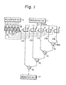
- Fig. 1 shows an example of a parallel multiplying circuit using a conventional second Booth's algorithm to which the present invention can be applied.
- a multiplicand X consists of ten bits of (x 9 , x 80 ..., x 0 ) which is a 2's complement code
- a multiplier Y consists of ten bits of (y 9 , y 8 , ..., y 0 ) which is a 2's complement code and where the product (X - Y) of both of the multiplicand X and multiplier Y is obtained.
- a reference numeral 1 denotes a register in which the multiplicand X is stored and 2 indicates a register in which the multiplier Y is stored.
- the multiplicand X is supplied to selectors 3, 4, 5, 6, and 7.
- the lower significant two bits y 0 and y 1 of the multiplier Y and 0 are supplied to an encoder 8.
- the three bits y 1 , y 2 and Y 3 of the multiplier Y are supplied to an encoder 9.
- the three bits y 3 , y 4 and y 5 are supplied to an encoder 10.
- the three bits y 5 , y 6 and y 7 are supplied to an encoder 11.
- the three bits y 7 , y 8 and y 9 are supplied to an encoder 12.
- Each of the encoders 8 to 12 generates a 3-bit output.
- the selectors 3 to 7 are respectively controlled by these outputs, so that partial products PA, PB, PC, PD, and PE each of which consists of eleven bits are formed.
- selectors 3 to 7 perform the arithmetic operations of 1's complement and thereby to obtain negative values
- one bit is added to carry out the correction for performing the negative expression of 2's complement arithmetic operations, so that the number of bits of partial product becomes twelve.
- the partial products PA and PB which are respectively outputted from the selectors 3 and 4 are supplied to an adder 13.
- the output of the adder 13 and the partial product PC outputted from the selector 5 are supplied to an adder 14.
- the output of the adder 14 and the partial product PD outputted from the selector 6 are supplied to an adder 15.
- the output of the adder 15 and the partial product PE outputted from the selector 7 are supplied to an adder 16.
- a predetermined weight is imparted to each partial product from the selectors 3 to 7 and is added. Namely, the partial product PB is shifted to the left by two bits and is added to the partial product PA. Similarly, the partial products PC, PD and PE are respectively shifted to the left by two bits and are added to the addition outputs of the adders 13, 14 and 15 at the front stage, respectively.
- This shifting operation to the left by two bits upon addition can be executed only by shifting the bit locations of two addition inputs.
- the output of the adder 16 becomes the product (X - Y) and it is stored in a register 17.
- the selectors 3 to 7 and the four-stage adders 13 to 16 are interposed between the registers 1 and 17; while the encoders 8 to 12 and the selectors 3 to 7 and the four-stage adders 13 to 16 are interposed between the registers 2 and 17. Therefore, the delay time in the multiplication becomes large and a high-speed operation cannot be expected in standard devices such as CMOS, TTL, etc. As a result, there is a problem such that is is impossible to multiply a signal having a high data rate such as, for instance, a digital color video signal.
- registers 18 and 19, registers 20 and 21, registers 22 and 23, and registers 24 and 25 are respectively interposed on the two input sides of each of the adders 13, 14, 15, and 16. Further, in order to match the timings, a register 27 is interposed between the selector 5 and the register 21; registers 28 and 29 are interposed between the selector 6 and the register 23; and registers 30, 31 and 32 are interposed between the selector 7 and the register 25.
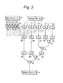
- Fig. 3 shows another arrangement of the case where the parallel multiplying circuit of Fig. 1 was constituted such that the pipeline processing can be performed.
- this circuit is constituted so as to execute the pipeline processing for every two stages of the adders.
- the adders 13 and 14 are combined as a set and the registers 18, 19 and 27 are provided on its input side.
- the adders 15 and 16 are combined as a set and the registers 22, 23 and 32 are provided on its input side.
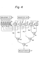
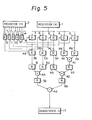
- the following arrangement is also possible. Namely, the partial products PA and PB which are outputted from the selectors 3 and 4 are added by an adder 41. This addition output and the partial product PC outputted from the selector 5 are added by an adder 42. The partial products PD and PE outputted from the selectors 6 and 7 are added by an adder 43. The outputs of the adders 42 and 43 are added by an adder 44.
- Such an arrangement whereby the adders 41 to 44 are connected like a tree as mentioned above can be constituted so as to perform the pipeline processing, as shown in Fig. 5, by respectively interposing registers 45, 46, 47, 48, 49, 50, 51, and 52 on the input and output sides of the adders 41 to 44 and by interposing registers 54, 55 and 56 for matching the timings.
- a digital multiplying circuit is constituted in the manner such that: a multiplicand is inputted; partial product signal generating circuits of the number corresponding to only the number of partial products which are needed are provided; the partial product signal generating circuits generate the partial product signals in accordance with the state of predetermined bits of a multiplier; each partial product signal is added; and thereby a multiplication output of the multiplicand is obtained.
- the pipeline processing is performed in the adding operation of each partial product signal and that the multiplier and multiplicand are delayed and the predetermined partial product signal generating circuits are arranged immediately before the adders which require the partial product signals, thereby obtaining the partial product signals.
- FIG. 6 An embodiment of the present invention shown in Fig. 6 relates to a digital multiplying circuit of which the invention was applied to the parallel multiplying circuit shown in Fig. 2.
- the multiplicand X of the 2's complement code consisting of ten bits, for example, stored in the register 1 is supplied to the selectors 3 and 4, and at the same time it is supplied to a register 61.
- Registers 62 and 63 are connected in series to the register 61.
- the registers 18 and 19 are connected to the input side of the adder 13 for adding the partial products PA and PB.
- the registers 20, 21, 22, 23, 24, and 25 are interposed on the respective input side of the adders 14, 15 and 16 for performing the additions of the partial products.
- the output of the adder 16 is supplied to the register 17. In this way, the adders 13 to 16 are constituted such that they are sandwiched by the registers, respectively.
- Each register in this embodiment of the invention holds the data for one clock interval of the varying frequency of at least one of the multiplicand X and multiplier Y.
- the multiplicand X is supplied from the register 61 to the selector 5.
- the partial product PC which is derived as the output of the selector 5 is supplied to the adder 14 through the register 21.
- the multiplicand X from the register 62 is supplied to the selector 6.
- the partial product PD which is obtained as the output of the selector 6 is supplied to the adder 15 through the register 23.
- the multiplicand X from the register 63 is supplied to the selector 7.
- the partial product PE from the selector 7 is supplied to the adder 16 through the register 25.
- the selectors 3 to 7 are constituted such that they are sandwiched by the registers, respectively.
- the multiplicand X which was sequentially delayed by the registers 61, 62 and 63 as well as the register 1 is supplied to the selectors 3 to 7; therefore, the signals to control these selectors are also similarly delayed.
- the lower significant two bits y 0 and y of the multiplier Y and 0 are supplied from the register 2 to the encoder 8.
- the three bits y 1 , y 2 and y 3 of the multiplier are supplied from the register 2 to the encoder 9.
- the selectors 3 and 4 are controlled by the outputs of the encoders 8 and 9.
- the three bits y 3 , y 4 and y 5 of the multiplier Y derived through registers 64, 65 and 67 each of which consists of one bit are supplied to the encoder 10.
- the selector 5 is controlled by the output of the encoder 10.
- the bit y 5 obtained through registers 67 and 73, the bit y- 6 obtained through registers 68 and 74, and the bit y 7 obtained through registers 70 and 76 are supplied to the encoder 11.
- the selector 6 is controlled by the output of the encoder 11.
- the bit y 7 obtained through registers 70, 76 and 79, the bit y 8 obtained through registers 71, 77 and 80, and the bit y 9 obtained through registers 72, 78 and 81 are supplied to the encoder 12.
- the selector 7 is controlled by the output of the encoder 12.
- the encoders 8 to 12 generate the outputs in accordance with the second Booth's algorithm.
- the predetermined partial products PA, PB, PC, PD, and PE are produced as the outputs of the selectors 3 to 7.
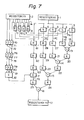
- the circuit arrangement shown in Fig. 8 is obtained.
- the multiplicand X is delayed by one clock interval by a register 82 and is supplied to the selector 5.
- the bits y 3 , y 4 and y 5 which were delayed by one clock interval by the registers 64, 65 and 66 are supplied to the encoder 10.
- the selector 5 is controlled by the output of the encoder 10.
- the multiplicand X is delayed by two clock interval by registers 83 and 84 and is supplied to the selector 6.
- the bits y 5 , Y 6 and y 7 which were delayed by two clock interval by the registers 67, 68, 69, 73, 74, and 75 are supplied to the encoder 11.
- the selector 6 is controlled by the output of the encoder 11.
- Fig. 8 which is equivalent to the arrangement of Fig. 2 is obtained by the above-mentioned replacement.
- the registers 61, 82 and 83 together delay the multiplicand X by one clock interval, while the registers 62 and 84 delay the respective outputs of the registers 61 and 83 by one clock interval.
- the registers 66 and 67 together delay the bit y 5 of the multiplier Y by one clock interval.
- the registers 69 and 70 together delay the bit Y7 of the multiplier Y by one clock interval.
- the registers 75 and 76 together delay the outputs of the registers 69 and 70 by one clock interval.
- each one register remains and the others can be omitted.
- the registers 82 and 83 are omitted, the register 84 is omitted, the registers 66 and 69 are omitted, and the register 75 is omitted, so that the arrangement of one embodiment of the invention shown in Fig. 6 is derived.
- the total number of bits of registers in the parallel multiplying circuit of Fig. 2 becomes 72 bits (i.e., 12 bits times six).
- the total number of bits of registers in the embodiment shown in Fig. 6 becomes 45 bits (i.e., 10 bits x 3 + 1 bit x 15), so that the registers corresponding to 27 bits can be saved.
- the register 27 of one stage, the registers 28 and 29 of two stages, ..., the registers of (i - 2) stages are sequentially needed with respect to the partial products from the partial product PC produced by the selector 5 to the partial products PD, PE, .... Since each of these registers consists of (m + 2) bits, the total number of necessary registers becomes
- this invention has a very larger effect of saving the number of registers as the bit width m is larger.
- Fig. 9 shows an arrangement of another embodiment of the invention.
- This embodiment relates to a digital multiplying circuit of which the invention was applied to the parallel multiplying circuit which can perform the pipeline processing for every two stages of adders as shown in Fig. 3.
- a main feature of this digital multiplying circuit is that the selectors 3, 4, 5, 6, and 7 for respectively producing the partial products PA, PB, PC, PD, and PE are arranged immediately before the adders 13, 14, 15, and 16.
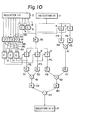
- Fig. 10 shows further another embodiment of the invention.
- This embodiment relates to a digital multiplying circuit of which the invention was applied to the circuit arrangement for adding the partial products like a tree as shown in Fig. 5.
- a feature of this digital multiplying circuit is that: the registers 54, 55 and 56 in Fig. 5 are collected as the one register 56; the multiplicand X from the register 56 is supplied to the selectors 5, 6 and 7; and the necessary bits in the multiplier Y are supplied through registers 91, 92, 93, 94, 95, 96, and 97 each consisting of one bit to the encoders 10, 11 and 12 for controlling the selectors 5, 6 and 7.
- the number of registers can be also saved.
- the invention is not limited to a parallel multiplying circuit using the second Booth's algorithm, but can be also applied to a parallel multiplying circuit using the first Booth's algorithm and to a parallel multiplying circuit which does not use a Booth's algorithm.
- a parallel multiplying circuit which can perform the pipeline processing and can carry out the operation by a high speed clock, it is possible to realize a digital multiplying circuit in which the number of bits of registers is remarkably reduced than a conventional arrangement and the circuit scale is small.
Landscapes
- Physics & Mathematics (AREA)
- General Physics & Mathematics (AREA)
- Engineering & Computer Science (AREA)
- Computational Mathematics (AREA)
- Mathematical Analysis (AREA)
- Mathematical Optimization (AREA)
- Pure & Applied Mathematics (AREA)
- Theoretical Computer Science (AREA)
- Computing Systems (AREA)
- General Engineering & Computer Science (AREA)
- Complex Calculations (AREA)
Applications Claiming Priority (2)
| Application Number | Priority Date | Filing Date | Title |
|---|---|---|---|
| JP175881/83 | 1983-09-22 | ||
| JP58175881A JPH0640301B2 (ja) | 1983-09-22 | 1983-09-22 | 並列乗算回路 |
Publications (3)
| Publication Number | Publication Date |
|---|---|
| EP0137386A2 true EP0137386A2 (de) | 1985-04-17 |
| EP0137386A3 EP0137386A3 (en) | 1985-08-21 |
| EP0137386B1 EP0137386B1 (de) | 1988-08-10 |
Family
ID=16003837
Family Applications (1)
| Application Number | Title | Priority Date | Filing Date |
|---|---|---|---|
| EP84111298A Expired EP0137386B1 (de) | 1983-09-22 | 1984-09-21 | Digitale Multiplizierschaltung |
Country Status (5)
| Country | Link |
|---|---|
| US (1) | US4706211A (de) |
| EP (1) | EP0137386B1 (de) |
| JP (1) | JPH0640301B2 (de) |
| CA (1) | CA1219955A (de) |
| DE (1) | DE3473364D1 (de) |
Cited By (2)
| Publication number | Priority date | Publication date | Assignee | Title |
|---|---|---|---|---|
| US4679164A (en) * | 1984-12-17 | 1987-07-07 | The United States Of America As Represented By The Secretary Of The Army | Digital high speed programmable convolver |
| EP0349819A1 (de) * | 1988-07-05 | 1990-01-10 | Siemens Aktiengesellschaft | In integrierter Schaltungstechnik ausgeführtes digitales neuronales Netz |
Families Citing this family (13)
| Publication number | Priority date | Publication date | Assignee | Title |
|---|---|---|---|---|
| JPH0816903B2 (ja) * | 1986-09-17 | 1996-02-21 | 富士通株式会社 | 積和演算回路 |
| US4831577A (en) * | 1986-09-17 | 1989-05-16 | Intersil, Inc. | Digital multiplier architecture with triple array summation of partial products |
| US4864529A (en) * | 1986-10-09 | 1989-09-05 | North American Philips Corporation | Fast multiplier architecture |
| US5001651A (en) * | 1986-11-10 | 1991-03-19 | Auto-Trol Technology Corporation | Method and apparatus for interpolating groups of pixels on a scan line |
| US4839847A (en) * | 1987-04-14 | 1989-06-13 | Harris Corp. | N-clock, n-bit-serial multiplier |
| US5136593A (en) * | 1989-10-30 | 1992-08-04 | Carnegie-Mellon University | Apparatus and method for fixed delay tree search |
| JP2597736B2 (ja) * | 1990-07-17 | 1997-04-09 | 株式会社東芝 | 高速乗算器 |
| JPH096614A (ja) * | 1995-06-21 | 1997-01-10 | Sanyo Electric Co Ltd | データ処理装置 |
| US6484193B1 (en) * | 1999-07-30 | 2002-11-19 | Advanced Micro Devices, Inc. | Fully pipelined parallel multiplier with a fast clock cycle |
| US7424506B2 (en) * | 2001-03-31 | 2008-09-09 | Durham Logistics Llc | Architecture and related methods for efficiently performing complex arithmetic |
| EP1623307B1 (de) * | 2003-05-09 | 2015-07-01 | QUALCOMM Incorporated | Prozessorreduktionseinheit zum akkumulieren mehrerer operanden mit oder ohne sättigung |
| US8074051B2 (en) * | 2004-04-07 | 2011-12-06 | Aspen Acquisition Corporation | Multithreaded processor with multiple concurrent pipelines per thread |
| KR102604087B1 (ko) | 2016-06-24 | 2023-11-21 | 삼성디스플레이 주식회사 | 윈도우 및 이를 포함하는 표시 장치 |
Family Cites Families (2)
| Publication number | Priority date | Publication date | Assignee | Title |
|---|---|---|---|---|
| US3515344A (en) * | 1966-08-31 | 1970-06-02 | Ibm | Apparatus for accumulating the sum of a plurality of operands |
| US4616330A (en) * | 1983-08-25 | 1986-10-07 | Honeywell Inc. | Pipelined multiply-accumulate unit |
-
1983
- 1983-09-22 JP JP58175881A patent/JPH0640301B2/ja not_active Expired - Lifetime
-
1984
- 1984-09-17 US US06/651,155 patent/US4706211A/en not_active Expired - Lifetime
- 1984-09-17 CA CA000463341A patent/CA1219955A/en not_active Expired
- 1984-09-21 DE DE8484111298T patent/DE3473364D1/de not_active Expired
- 1984-09-21 EP EP84111298A patent/EP0137386B1/de not_active Expired
Non-Patent Citations (2)
| Title |
|---|
| IEE 5th EUROPEAN SOLID STATE CIRCUITS CONFERENCE, Southampton, GB, 18th-21st September 1979, pages 110-112; T. TAKAHASHI et al.: "A high speed multiplier using subnanosecond bipolar VLSI technologies" * |
| IEEE JOURNAL OF SOLID-STATE CIRCUITS, vol. SC-18, no. 3, June 1983, pages 280-285, IEEE, New York, US; P. DRAHEIM: "Digital signal processing for video applications" * |
Cited By (2)
| Publication number | Priority date | Publication date | Assignee | Title |
|---|---|---|---|---|
| US4679164A (en) * | 1984-12-17 | 1987-07-07 | The United States Of America As Represented By The Secretary Of The Army | Digital high speed programmable convolver |
| EP0349819A1 (de) * | 1988-07-05 | 1990-01-10 | Siemens Aktiengesellschaft | In integrierter Schaltungstechnik ausgeführtes digitales neuronales Netz |
Also Published As
| Publication number | Publication date |
|---|---|
| EP0137386B1 (de) | 1988-08-10 |
| EP0137386A3 (en) | 1985-08-21 |
| CA1219955A (en) | 1987-03-31 |
| DE3473364D1 (en) | 1988-09-15 |
| JPH0640301B2 (ja) | 1994-05-25 |
| JPS6068433A (ja) | 1985-04-19 |
| US4706211A (en) | 1987-11-10 |
Similar Documents
| Publication | Publication Date | Title |
|---|---|---|
| EP0137386A2 (de) | Digitale Multiplizierschaltung | |
| US5754459A (en) | Multiplier circuit design for a programmable logic device | |
| US3524977A (en) | Binary multiplier employing multiple input threshold gate adders | |
| US3648038A (en) | Apparatus and method for obtaining the reciprocal of a number and the quotient of two numbers | |
| US20190303103A1 (en) | Common factor mass multiplication circuitry | |
| US4745570A (en) | Binary multibit multiplier | |
| US5323338A (en) | Pseudo-random sequence generators | |
| US6065033A (en) | Wallace-tree multipliers using half and full adders | |
| JP3345894B2 (ja) | 浮動小数点乗算器 | |
| US5177703A (en) | Division circuit using higher radices | |
| Dadda | Some schemes for fast serial input multipliers | |
| US4638449A (en) | Multiplier architecture | |
| US4628472A (en) | Binary multiplier using ternary code | |
| Leela et al. | A novel design of high speed multiplier using hybrid adder technique | |
| US4389723A (en) | High-speed pattern generator | |
| US4677583A (en) | Apparatus for decimal multiplication | |
| US5781462A (en) | Multiplier circuitry with improved storage and transfer of booth control coefficients | |
| KR0147942B1 (ko) | 승산기에서의 부스 레코딩회로 | |
| EP0326414A2 (de) | Hochgeschwindigkeits-Multiplizierer | |
| EP0129039B1 (de) | Architektur eines Multiplizierers | |
| JPS61246837A (ja) | 並列乗算器 | |
| KR950010451B1 (ko) | 그룹 트리구조 알고리즘(GTSM ; Group Tree Structure Method)을 적용한 고속 승산기 | |
| JP2728958B2 (ja) | 演算処理装置及び方法 | |
| KR0153963B1 (ko) | 수정형 부스승산기에 있어서 부분곱 행 생성회로 | |
| KR100362186B1 (ko) | 멀티플렉서를이용한직렬부스승산기 |
Legal Events
| Date | Code | Title | Description |
|---|---|---|---|
| PUAI | Public reference made under article 153(3) epc to a published international application that has entered the european phase |
Free format text: ORIGINAL CODE: 0009012 |
|
| AK | Designated contracting states |
Designated state(s): DE FR GB NL |
|
| PUAL | Search report despatched |
Free format text: ORIGINAL CODE: 0009013 |
|
| AK | Designated contracting states |
Designated state(s): DE FR GB NL |
|
| 17P | Request for examination filed |
Effective date: 19851128 |
|
| 17Q | First examination report despatched |
Effective date: 19861127 |
|
| GRAA | (expected) grant |
Free format text: ORIGINAL CODE: 0009210 |
|
| AK | Designated contracting states |
Kind code of ref document: B1 Designated state(s): DE FR GB NL |
|
| REF | Corresponds to: |
Ref document number: 3473364 Country of ref document: DE Date of ref document: 19880915 |
|
| ET | Fr: translation filed | ||
| PLBE | No opposition filed within time limit |
Free format text: ORIGINAL CODE: 0009261 |
|
| STAA | Information on the status of an ep patent application or granted ep patent |
Free format text: STATUS: NO OPPOSITION FILED WITHIN TIME LIMIT |
|
| 26N | No opposition filed | ||
| GBPC | Gb: european patent ceased through non-payment of renewal fee |
Effective date: 19950921 |
|
| GBPC | Gb: european patent ceased through non-payment of renewal fee |
Free format text: DELETE IN JOURNAL 5587, PAGE 2475 CEASED IN ERROR |
|
| PGFP | Annual fee paid to national office [announced via postgrant information from national office to epo] |
Ref country code: GB Payment date: 20010919 Year of fee payment: 18 |
|
| PGFP | Annual fee paid to national office [announced via postgrant information from national office to epo] |
Ref country code: DE Payment date: 20011009 Year of fee payment: 18 |
|
| REG | Reference to a national code |
Ref country code: GB Ref legal event code: IF02 |
|
| PG25 | Lapsed in a contracting state [announced via postgrant information from national office to epo] |
Ref country code: GB Free format text: LAPSE BECAUSE OF NON-PAYMENT OF DUE FEES Effective date: 20020921 |
|
| PG25 | Lapsed in a contracting state [announced via postgrant information from national office to epo] |
Ref country code: DE Free format text: LAPSE BECAUSE OF NON-PAYMENT OF DUE FEES Effective date: 20030401 |
|
| GBPC | Gb: european patent ceased through non-payment of renewal fee |
Effective date: 20020921 |
|
| PGFP | Annual fee paid to national office [announced via postgrant information from national office to epo] |
Ref country code: FR Payment date: 20030909 Year of fee payment: 20 |
|
| PGFP | Annual fee paid to national office [announced via postgrant information from national office to epo] |
Ref country code: NL Payment date: 20030922 Year of fee payment: 20 |
|
| PG25 | Lapsed in a contracting state [announced via postgrant information from national office to epo] |
Ref country code: NL Free format text: LAPSE BECAUSE OF EXPIRATION OF PROTECTION Effective date: 20040921 |
|
| NLV7 | Nl: ceased due to reaching the maximum lifetime of a patent |
Effective date: 20040921 |