EP0137747A2 - Verfahren zur Herstellung kornorientierter Stähle - Google Patents
Verfahren zur Herstellung kornorientierter Stähle Download PDFInfo
- Publication number
- EP0137747A2 EP0137747A2 EP84306258A EP84306258A EP0137747A2 EP 0137747 A2 EP0137747 A2 EP 0137747A2 EP 84306258 A EP84306258 A EP 84306258A EP 84306258 A EP84306258 A EP 84306258A EP 0137747 A2 EP0137747 A2 EP 0137747A2
- Authority
- EP
- European Patent Office
- Prior art keywords
- strip
- sheet
- discharge
- probe
- ablation
- Prior art date
- Legal status (The legal status is an assumption and is not a legal conclusion. Google has not performed a legal analysis and makes no representation as to the accuracy of the status listed.)
- Granted
Links
Images
Classifications
-
- C—CHEMISTRY; METALLURGY
- C21—METALLURGY OF IRON
- C21D—MODIFYING THE PHYSICAL STRUCTURE OF FERROUS METALS; GENERAL DEVICES FOR HEAT TREATMENT OF FERROUS OR NON-FERROUS METALS OR ALLOYS; MAKING METAL MALLEABLE, e.g. BY DECARBURISATION OR TEMPERING
- C21D8/00—Modifying the physical properties of ferrous metals or ferrous alloys by deformation combined with, or followed by, heat treatment
- C21D8/12—Modifying the physical properties of ferrous metals or ferrous alloys by deformation combined with, or followed by, heat treatment during manufacturing of articles with special electromagnetic properties
- C21D8/1294—Modifying the physical properties of ferrous metals or ferrous alloys by deformation combined with, or followed by, heat treatment during manufacturing of articles with special electromagnetic properties involving a localised treatment
-
- C—CHEMISTRY; METALLURGY
- C21—METALLURGY OF IRON
- C21D—MODIFYING THE PHYSICAL STRUCTURE OF FERROUS METALS; GENERAL DEVICES FOR HEAT TREATMENT OF FERROUS OR NON-FERROUS METALS OR ALLOYS; MAKING METAL MALLEABLE, e.g. BY DECARBURISATION OR TEMPERING
- C21D1/00—General methods or devices for heat treatment, e.g. annealing, hardening, quenching or tempering
- C21D1/06—Surface hardening
- C21D1/09—Surface hardening by direct application of electrical or wave energy; by particle radiation
-
- H—ELECTRICITY
- H01—ELECTRIC ELEMENTS
- H01F—MAGNETS; INDUCTANCES; TRANSFORMERS; SELECTION OF MATERIALS FOR THEIR MAGNETIC PROPERTIES
- H01F1/00—Magnets or magnetic bodies characterised by the magnetic materials therefor; Selection of materials for their magnetic properties
- H01F1/01—Magnets or magnetic bodies characterised by the magnetic materials therefor; Selection of materials for their magnetic properties of inorganic materials
- H01F1/03—Magnets or magnetic bodies characterised by the magnetic materials therefor; Selection of materials for their magnetic properties of inorganic materials characterised by their coercivity
- H01F1/12—Magnets or magnetic bodies characterised by the magnetic materials therefor; Selection of materials for their magnetic properties of inorganic materials characterised by their coercivity of soft-magnetic materials
- H01F1/14—Magnets or magnetic bodies characterised by the magnetic materials therefor; Selection of materials for their magnetic properties of inorganic materials characterised by their coercivity of soft-magnetic materials metals or alloys
- H01F1/16—Magnets or magnetic bodies characterised by the magnetic materials therefor; Selection of materials for their magnetic properties of inorganic materials characterised by their coercivity of soft-magnetic materials metals or alloys in the form of sheets
Definitions
- This invention relates to the production of grain orientated steel.
- Sheet or strip of grain orientated steel for electrical purposes is of course well known. Such sheet or strip is used for electromagnetic applications eg. to form a magnetic circuit in electric machines.
- the sheet or strip is typically produced from steel containing silicon typically in concentrations within the range 2 - 4% weight. Processing of the silicon steel by working and thermal treatment in known manner promotes preferential growth of some grains within the steel in order to obtain large grains having predominantly (110) [0013 Miller Indices and to inhibit the growth of the remaining grains. This of course leads to strong orientation of the grains with strongly enhanced magnetic characteristics for the purposes for which the steel is intended.
- a problem associated with the production of such grain orientated steel is that production of optimum alignment of the grain leads at the same time to grains of a larger than optimum size. Such large grain size leads to significant power loss problems. Magnetic domain wall spacing within the grains becomes large so that in use rapid movement of the domain walls (caused by the greater distance to be moved by the domain walls in unit time) create severe micro-eddy currents,in turn causing power losses.
- a method of treating grain orientated steel sheet or strip to refine domain spacing by subjecting the steel sheet or strip to electrical discharge to create a line of surface ablation and stress thereacross.
- apparatus for treating grain orientated steel sheet or strip to refine the domain spacing comprising an electric discharge probe adapted to be located above the surface of a grain orientated sheet or strip and means for causing the probe to discharge so as to create a line of surface ablation and stress on the sheet or strip.
- the line of ablation can be constituted by a succession of discharge spots, or alternatively a continuous line of ablation can be created.
- electrical steel sheet or strip of the kind to which this invention relates typically having a thickness of between 0.20 to 0.35 mm
- the line of ablation created by the discharge provides a simulated grain boundary effect through the thickness of the metal.
- the discharge creates atomic magnitude disruption at and below the metal surface, and in addition a thermal stress field is set up below the surface through the thickness of the sheet or strip effective as a simulated grain boundary.
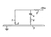
- the probe 1 is located with a gap 2 of between 2 and 3 mm above the surface of the sheet 3 which is of a thickness between 0.2.0 and 0.35 mm (although the gap 2 can be less, for example down to 0.5 mm) and is raised to a high voltage supply of - 12 KV with respect to the sheet in order to cause a spark to discharge from the probe to the sheet.
- the voltage for discharge will be of the order of 3000 to 10,000 volts. It is to be observed that although grain orientated electrical steel carries an insulating coating as a matter of course, high voltage of this magnitude, necessary for the spark to traverse the air gap between the probe and the steel sheet, will also be quite adequate to effect the breakdown of the insulating coating.
- a gap of between 1 to 3 mm is sufficiently large to enable a relative constancy of spacing between the probe and the sheet to be maintained during movement of the probe relative to the sheet.
- a capacitor 4 is connected between the probe and the sheet, the capacitor being of a moderate size, for example somewhere between 1000 and 10,000 pf.
- the energy delivered is of the order of t CV joules where C is the capacitance of the capacitor and V is the voltage across the gap between the probe and the sheet. It is to be noted that regulation of the gap between the probe and the sheet (and thus the discharge voltage) or the capacitance of the capacitor will enable regulation of the delivered energy.
- a circuit of the kind illustrated in the Figure will act in practise as a relaxation oscillator so that spark discharge will occur at the rate related to a time constant R, where R is the resistance of a resistor 5 connected in the power supply line, and the relaxation between the power supply of 12 KV and the breakdown potential of the gap between the probe and the sheet. Regulation of the energy delivery rate can also be controlled by regulation of the value given to a low value resistor 6 connected in series with the capacitor 4.
- Adjustment of the gap between probe 1 and sheet 2 the value of the capacitor 4, the value of the large resistor 5, the value of the power supply, and the value of the small resistor 6 give a very wide control of the production of ablation spots from the discharge. If the probe is moved in line along or across the sheet a line of ablation spots, producing a barrier wall simulating the effect of a grain boundary will be produced, this barrier wall acting as a domain spacing refining system. Clearly the probe can be moved successively across the sheet to produce a succession of such lines and a domain spacing refining system throughout the sheet.
- a continuous arc discharge can be produced so that a continuous line of ablation can be drawn across the surface of the sheet.
- the discharge spots can be provided at a fixed power supply by use of a trigger mechanism to discharge the capacitor rather than rely on the natural breakdown voltage of the gap between the probe and the sheet.
- a multiple array of probes can be utilised for simultaneous actuation, the probes being spaced a predetermined distance apart and moved together across the sheet.
- the spacing of the probes in this case would be such as to apply lines of barrier walls at a spacing found to be most suitable for the particular grain orientated steel concerned.
- the losses referred to in the following table 1 part B are . measured at an induction of 1.7 Tesla and 50 Hertz.
- An Epstein sample of Hi B type grain oriented silicon steel was scribed by the method described above using an electrode/strip gap of 1.81mm, a resistor of value 1M ⁇ , a capacitor of value 2500pF, and a traverse rate of electrode across the strip of 0.5cm/sec.
- the permeability of the sample was 1.96 and the power loss was 1.276W/kg. After treatment the loss value was reduced by 10.0% to a value of 1.148W/kg.
- An Epstein sample of Hi B type grain oriented silicon steel was scribed by the method described above using an electrode/strip gap of 0.86mm, a resistor of value IMQ, a capacitor of value 2500pF, and a traverse rate of electrode across the strip of 0.5cm/sec.
- the permeability of the sample was 1.96 and the power loss was 1.242W/kg. After treatment the loss value was reduced by 15.9% to a value of 1.044W/kg.
- the ablation energy in this case was lower than that employed in Example 1 as indicated by the lower electrode/strip gap (0.86mm compared to 1.81 mm).
- An Epstein sample of Hi B type grain oriented silicon steel was scribed by the method described above using an electrode/strip gap of 1.14mm, a resistor of value 5MQ, a capacitor of value 2500pF, and a traverse rate of electrode across the strip of 0.5cm/sec.
- the permeability of the sample Prior to treatment the permeability of the sample was 1.96 and the power loss was 1.314 W/kg. After treatment the loss value was reduced by 11.0% to a value of 1.170W/kg.
- An Epstein sample of Hi B type grain oriented silicon steel was scribed by the method described above using an electrode/strip gap of 1.14mm, a resistor of value 200kQ, a capacitor of value 2500pF and a traverse rate of electrode across the strip of 0.5cm/sec.
- the permeability of the sample was 1.96 and the power loss was 1.288W/kg. After treatment the loss value was reduced by 11.7% to a value of 1.137W/kg.
- An Epstein sample of Hi B type grain oriented silicon steel was scribed by the method described above using an electrode/strip gap of 1.14mm, a resistor of value IMQ, a capacitor of value 2500pF, and a traverse rate of electrode across the strip of 0.5cm/sec.
- the permeability of the sample was 1.93 and the power loss was 1.148W/kg. After treatment the loss value was reduced by 9.1% to a value of 1.043W/kg.
- An Epstein sample of Hi B type grain oriented silicon steel was scribed by the method described above using an electrode/strip gap of 1.14mm, a resistor of value IMQ, a capacitor of value 2500pF, and a traverse rate of electrode across the strip of 10cm/sec.
- the permeability of the sample was 1.96 and the power loss was 1.172W/kg. After treatment the loss value was reduced by 7.3% to a value of 1.086W/kg.
- Examples 7 and 8 give data for higher and lower ablation energies than employed in Examples 1 - 6, as indicated by the values of electrode/strip gap, 0.42 and 2.2mm compared to 0.86 - 1.81mm.
- An Epstein sample of Hi B type grain oriented silicon steel was scribed by the method described above using an electrode/strip gap of 0.42mm, a resistor of value I MQ, a capacitor of value 2500pF, and a traverse rate of electrode across the strip of 2.5cm/sec.
- the permeability of the sample was 1.93 and the power loss was 1.190 W/kg. After treatment the loss value was reduced by 7.0% to a value of 1.134W/kg.
- An Epstein sample of Hi B type grain oriented silicon steel was scribed by the method described baveo using an electrode/strip gap of 2.2mm, a resistor of value 1M ⁇ , a capacitor of value 2500pF, and a traverse rate of electrode across the strip of 2.5cm/sec.
- the permeability of the sample was 1.93 and the power loss was 1.320W/kg. After treatment the loss value was reduced by 6.8% to a value of 1.230W/kg.
Landscapes
- Chemical & Material Sciences (AREA)
- Engineering & Computer Science (AREA)
- Physics & Mathematics (AREA)
- Materials Engineering (AREA)
- Organic Chemistry (AREA)
- Thermal Sciences (AREA)
- Crystallography & Structural Chemistry (AREA)
- Mechanical Engineering (AREA)
- Metallurgy (AREA)
- Electromagnetism (AREA)
- Manufacturing & Machinery (AREA)
- Dispersion Chemistry (AREA)
- Power Engineering (AREA)
- Manufacturing Of Steel Electrode Plates (AREA)
- Chemical Treatment Of Metals (AREA)
- Heat Treatment Of Sheet Steel (AREA)
- ing And Chemical Polishing (AREA)
- Electrical Discharge Machining, Electrochemical Machining, And Combined Machining (AREA)
Applications Claiming Priority (2)
| Application Number | Priority Date | Filing Date | Title |
|---|---|---|---|
| GB838324643A GB8324643D0 (en) | 1983-09-14 | 1983-09-14 | Production of grain orientated steel |
| GB8324643 | 1983-09-14 |
Publications (3)
| Publication Number | Publication Date |
|---|---|
| EP0137747A2 true EP0137747A2 (de) | 1985-04-17 |
| EP0137747A3 EP0137747A3 (en) | 1985-09-25 |
| EP0137747B1 EP0137747B1 (de) | 1989-03-01 |
Family
ID=10548790
Family Applications (1)
| Application Number | Title | Priority Date | Filing Date |
|---|---|---|---|
| EP84306258A Expired EP0137747B1 (de) | 1983-09-14 | 1984-09-13 | Verfahren zur Herstellung kornorientierter Stähle |
Country Status (6)
| Country | Link |
|---|---|
| US (1) | US4652316A (de) |
| EP (1) | EP0137747B1 (de) |
| JP (1) | JPS6089523A (de) |
| DE (1) | DE3476897D1 (de) |
| GB (2) | GB8324643D0 (de) |
| NO (1) | NO163785C (de) |
Cited By (5)
| Publication number | Priority date | Publication date | Assignee | Title |
|---|---|---|---|---|
| EP0220940A3 (en) * | 1985-10-24 | 1987-12-16 | Kawasaki Steel Corporation | Process and apparatus for improvement of iron loss of electromagnetic steel sheet or amorphous material |
| US4767469A (en) * | 1987-05-08 | 1988-08-30 | Allegheny Ludlum Corporation | Electrical discharge scribing for improving core loss of grain-oriented silicon steel |
| US4780155A (en) * | 1987-05-08 | 1988-10-25 | Allegheny Ludlum Corporation | Capacitive electrical discharge scribing for improving core loss of grain-oriented silicon steel |
| EP0304740A3 (en) * | 1987-08-22 | 1989-03-29 | British Steel Plc | Processing grain oriented electrical steel |
| EP0332041A3 (de) * | 1988-03-05 | 1990-08-22 | British Steel plc | Behandlung von kornorientiertem Elektrostahl |
Families Citing this family (14)
| Publication number | Priority date | Publication date | Assignee | Title |
|---|---|---|---|---|
| JPS62151511A (ja) * | 1985-12-26 | 1987-07-06 | Kawasaki Steel Corp | 方向性珪素鋼板の鉄損低減方法 |
| JPH0772300B2 (ja) * | 1985-10-24 | 1995-08-02 | 川崎製鉄株式会社 | 低鉄損方向性珪素鋼板の製造方法 |
| US4728083A (en) * | 1985-12-16 | 1988-03-01 | Allegheny Ludlum Corporation | Method and apparatus for scribing grain-oriented silicon steel strip |
| JPH0672264B2 (ja) * | 1985-12-26 | 1994-09-14 | 川崎製鉄株式会社 | 低鉄損方向性けい素鋼板の製造方法 |
| JPH0672265B2 (ja) * | 1985-12-26 | 1994-09-14 | 川崎製鉄株式会社 | 方向性けい素鋼板の鉄損改善方法 |
| JPH0772301B2 (ja) * | 1985-12-26 | 1995-08-02 | 川崎製鉄株式会社 | 方向性けい素鋼板の鉄損低減方法 |
| US4909864A (en) * | 1986-09-16 | 1990-03-20 | Kawasaki Steel Corp. | Method of producing extra-low iron loss grain oriented silicon steel sheets |
| US4931613A (en) * | 1987-05-08 | 1990-06-05 | Allegheny Ludlum Corporation | Electrical discharge scribing for improving core loss of grain-oriented silicon steel |
| US4915750A (en) * | 1988-03-03 | 1990-04-10 | Allegheny Ludlum Corporation | Method for providing heat resistant domain refinement of electrical steels to reduce core loss |
| US5123977A (en) * | 1989-07-19 | 1992-06-23 | Allegheny Ludlum Corporation | Method and apparatus for refining the domain structure of electrical steels by local hot deformation and product thereof |
| RU2176578C1 (ru) * | 2000-05-17 | 2001-12-10 | Поляченко Анатолий Васильевич | Способ упрочнения чугунных деталей |
| RU2405841C1 (ru) * | 2009-08-03 | 2010-12-10 | Открытое акционерное общество "Новолипецкий металлургический комбинат" | Способ производства листовой анизотропной электротехнической стали |
| DE102014102033B4 (de) * | 2014-02-18 | 2016-09-22 | Gottfried Wilhelm Leibniz Universität Hannover | Verfahren zum konduktiven Erwärmen eines Blechs und Erwärmungseinrichtung dafür |
| CN109202192B (zh) * | 2018-10-31 | 2019-09-17 | 清华大学 | 微细电火花伺服扫描加工参数优选方法及系统 |
Family Cites Families (17)
| Publication number | Priority date | Publication date | Assignee | Title |
|---|---|---|---|---|
| GB817408A (en) * | 1956-12-13 | 1959-07-29 | Sparcatron Ltd | Improvements in and relating to apparatus for the production of hardened surfaces |
| DE696739C (de) * | 1937-10-21 | 1940-09-27 | Metallgesellschaft Akt Ges | lischen Werkstuecken |
| CH381717A (de) * | 1957-01-12 | 1964-09-15 | Lihl Franz Prof Dr | Verfahren zur Hochhärtung von nichtaustenitischen Stählen |
| GB893233A (en) * | 1958-10-24 | 1962-04-04 | Ass Elect Ind | Improvements relating to the surface heating of metals |
| FR1265272A (fr) * | 1960-05-18 | 1961-06-30 | Citroen Sa Andre | Appareil pour le durcissement superficiel des métaux par étincelles |
| DE1496167B2 (de) * | 1964-05-28 | 1972-11-09 | Ritzerfeld, Gerhard, 1000 Berlin | Verfahren zur herstellung von druckformfolien fuer das elektrostatische druckverfahren |
| US3281289A (en) * | 1964-07-31 | 1966-10-25 | Daniel I Gordon | Method of producing magnetic cores |
| GB1112259A (en) * | 1966-02-22 | 1968-05-01 | Agemaspark Holdings Ltd | Spark erosion machines |
| NL6808468A (de) * | 1968-06-15 | 1969-12-17 | ||
| DE1804208B1 (de) * | 1968-10-17 | 1970-11-12 | Mannesmann Ag | Verfahren zur Herabsetzung der Wattverluste von kornorientierten Elektroblechen,insbesondere von Wuerfeltexturblechen |
| JPS5423647B2 (de) * | 1974-04-25 | 1979-08-15 | ||
| DE2553385A1 (de) * | 1975-11-27 | 1977-06-08 | Siemens Ag | Verfahren zum herstellen von praezisen mustern in duennen metallisierungen auf kunststoffolien |
| SU652230A1 (ru) * | 1977-10-04 | 1979-03-15 | Институт физики металлов УНЦ АН СССР | Способ термообработки электротехнической стали |
| JPS5518566A (en) * | 1978-07-26 | 1980-02-08 | Nippon Steel Corp | Improving method for iron loss characteristic of directional electrical steel sheet |
| GB2104432B (en) * | 1981-07-17 | 1985-12-11 | Nippon Steel Corp | Method and apparatus for reducing the watt loss of a grain-oriented electromagnetic steel sheet and a grain-oriented electromagnetic steel sheet having a low watt loss |
| JPS58144424A (ja) * | 1982-02-19 | 1983-08-27 | Kawasaki Steel Corp | 低鉄損方向性電磁鋼板の製造方法 |
| US4554029A (en) * | 1982-11-08 | 1985-11-19 | Armco Inc. | Local heat treatment of electrical steel |
-
1983
- 1983-09-14 GB GB838324643A patent/GB8324643D0/en active Pending
-
1984
- 1984-08-31 US US06/645,834 patent/US4652316A/en not_active Expired - Lifetime
- 1984-09-12 GB GB08423012A patent/GB2146567B/en not_active Expired
- 1984-09-13 NO NO843625A patent/NO163785C/no unknown
- 1984-09-13 JP JP59192441A patent/JPS6089523A/ja active Pending
- 1984-09-13 DE DE8484306258T patent/DE3476897D1/de not_active Expired
- 1984-09-13 EP EP84306258A patent/EP0137747B1/de not_active Expired
Cited By (8)
| Publication number | Priority date | Publication date | Assignee | Title |
|---|---|---|---|---|
| EP0220940A3 (en) * | 1985-10-24 | 1987-12-16 | Kawasaki Steel Corporation | Process and apparatus for improvement of iron loss of electromagnetic steel sheet or amorphous material |
| US4772338A (en) * | 1985-10-24 | 1988-09-20 | Kawasaki Steel Corporation | Process and apparatus for improvement of iron loss of electromagnetic steel sheet or amorphous material |
| US4767469A (en) * | 1987-05-08 | 1988-08-30 | Allegheny Ludlum Corporation | Electrical discharge scribing for improving core loss of grain-oriented silicon steel |
| US4780155A (en) * | 1987-05-08 | 1988-10-25 | Allegheny Ludlum Corporation | Capacitive electrical discharge scribing for improving core loss of grain-oriented silicon steel |
| EP0290175A1 (de) * | 1987-05-08 | 1988-11-09 | Allegheny Ludlum Corporation | Ritzen mittels kapazitiver elektrischer Entladungen zum Verbessern der Eisenverluste eines kornorientierten Siliziumstahls |
| EP0290174A1 (de) * | 1987-05-08 | 1988-11-09 | Allegheny Ludlum Corporation | Ritzen mittels elektrischer Entladungen zum Verbessern der Eisenverluste eines kornorientierten Siliziumstahls |
| EP0304740A3 (en) * | 1987-08-22 | 1989-03-29 | British Steel Plc | Processing grain oriented electrical steel |
| EP0332041A3 (de) * | 1988-03-05 | 1990-08-22 | British Steel plc | Behandlung von kornorientiertem Elektrostahl |
Also Published As
| Publication number | Publication date |
|---|---|
| GB2146567A (en) | 1985-04-24 |
| NO163785C (no) | 1990-07-18 |
| JPS6089523A (ja) | 1985-05-20 |
| GB2146567B (en) | 1987-09-09 |
| NO843625L (no) | 1985-03-15 |
| EP0137747B1 (de) | 1989-03-01 |
| GB8324643D0 (en) | 1983-10-19 |
| GB8423012D0 (en) | 1984-10-17 |
| EP0137747A3 (en) | 1985-09-25 |
| US4652316A (en) | 1987-03-24 |
| NO163785B (no) | 1990-04-09 |
| DE3476897D1 (en) | 1989-04-06 |
Similar Documents
| Publication | Publication Date | Title |
|---|---|---|
| EP0137747A2 (de) | Verfahren zur Herstellung kornorientierter Stähle | |
| US4931613A (en) | Electrical discharge scribing for improving core loss of grain-oriented silicon steel | |
| US5069428A (en) | Method and apparatus of continuous dynamic joule heating to improve magnetic properties and to avoid annealing embrittlement of ferro-magnetic amorphous alloys | |
| US4919733A (en) | Method for refining magnetic domains of electrical steels to reduce core loss | |
| DE3851678T2 (de) | Verarbeitung von kornorientiertem "elektrischen" Stahl. | |
| US4915750A (en) | Method for providing heat resistant domain refinement of electrical steels to reduce core loss | |
| ES2014902A6 (es) | Metodo, dispositivo y material para producir objetos tridimensionales. | |
| Beckley et al. | Domain control by spark ablation | |
| DE2507053A1 (de) | Verfahren und vorrichtung zur elektroerosionsbearbeitung | |
| US2759088A (en) | Method of rounding wire end | |
| EP0290174B1 (de) | Ritzen mittels elektrischer Entladungen zum Verbessern der Eisenverluste eines kornorientierten Siliziumstahls | |
| EP0290175B1 (de) | Ritzen mittels kapazitiver elektrischer Entladungen zum Verbessern der Eisenverluste eines kornorientierten Siliziumstahls | |
| Kahlon et al. | Electric spark toughening of cutting tools and steel components | |
| DE3131037C2 (de) | ||
| JPS6156825A (ja) | 放電加工方法および装置 | |
| Seely | Pulsed megagauss fields produced by laser-driven coils | |
| GB2054436A (en) | Electrical discharge machining using controlled low stray capacitances | |
| US3522116A (en) | Method of heat treating edges | |
| DE857839C (de) | Verfahren und Vorrichtung zum elektro-induktiven Erhitzen von Werkstuecken | |
| EP0101922B1 (de) | Verfahren und Vorrichtung zur Behandlung von ferromagnetischen Werkstoffen | |
| Williams et al. | Recent developments in the theory and design of electric spark machine tools | |
| US4924052A (en) | Processing grain-oriented "electrical" steel | |
| KR930010324B1 (ko) | 강자성 비정질 합금의 연속 쥴 열처리 방법 및 그 장치 | |
| DE859342C (de) | Einrichtung zur dielektrischen Behandlung von Gegenstaenden oder Stoffen durch Hochfrequenz mit selbsterregendem Hoch-frequenzgenerator | |
| DE1640503B2 (de) | Verfahren zum Widerstandsabgleich eines elektrischen Schichtwiderstandselements mit glasierter Widersstandsschicht |
Legal Events
| Date | Code | Title | Description |
|---|---|---|---|
| PUAI | Public reference made under article 153(3) epc to a published international application that has entered the european phase |
Free format text: ORIGINAL CODE: 0009012 |
|
| AK | Designated contracting states |
Designated state(s): BE DE FR IT NL SE |
|
| PUAL | Search report despatched |
Free format text: ORIGINAL CODE: 0009013 |
|
| AK | Designated contracting states |
Designated state(s): BE DE FR IT NL SE |
|
| 17P | Request for examination filed |
Effective date: 19860219 |
|
| 17Q | First examination report despatched |
Effective date: 19870402 |
|
| RAP1 | Party data changed (applicant data changed or rights of an application transferred) |
Owner name: BRITISH STEEL PLC |
|
| GRAA | (expected) grant |
Free format text: ORIGINAL CODE: 0009210 |
|
| AK | Designated contracting states |
Kind code of ref document: B1 Designated state(s): BE DE FR IT NL SE |
|
| PG25 | Lapsed in a contracting state [announced via postgrant information from national office to epo] |
Ref country code: NL Effective date: 19890301 |
|
| ITF | It: translation for a ep patent filed | ||
| REF | Corresponds to: |
Ref document number: 3476897 Country of ref document: DE Date of ref document: 19890406 |
|
| ET | Fr: translation filed | ||
| NLV1 | Nl: lapsed or annulled due to failure to fulfill the requirements of art. 29p and 29m of the patents act | ||
| PLBE | No opposition filed within time limit |
Free format text: ORIGINAL CODE: 0009261 |
|
| STAA | Information on the status of an ep patent application or granted ep patent |
Free format text: STATUS: NO OPPOSITION FILED WITHIN TIME LIMIT |
|
| 26N | No opposition filed | ||
| PGFP | Annual fee paid to national office [announced via postgrant information from national office to epo] |
Ref country code: BE Payment date: 19900821 Year of fee payment: 7 |
|
| PG25 | Lapsed in a contracting state [announced via postgrant information from national office to epo] |
Ref country code: BE Effective date: 19910930 |
|
| BERE | Be: lapsed |
Owner name: BRITISH STEEL P.L.C. Effective date: 19910930 |
|
| ITTA | It: last paid annual fee | ||
| REG | Reference to a national code |
Ref country code: FR Ref legal event code: TP |
|
| EAL | Se: european patent in force in sweden |
Ref document number: 84306258.9 |
|
| PGFP | Annual fee paid to national office [announced via postgrant information from national office to epo] |
Ref country code: FR Payment date: 19980810 Year of fee payment: 15 |
|
| PGFP | Annual fee paid to national office [announced via postgrant information from national office to epo] |
Ref country code: SE Payment date: 19980813 Year of fee payment: 15 |
|
| PGFP | Annual fee paid to national office [announced via postgrant information from national office to epo] |
Ref country code: DE Payment date: 19980826 Year of fee payment: 15 |
|
| PG25 | Lapsed in a contracting state [announced via postgrant information from national office to epo] |
Ref country code: SE Free format text: THE PATENT HAS BEEN ANNULLED BY A DECISION OF A NATIONAL AUTHORITY Effective date: 19990929 |
|
| EUG | Se: european patent has lapsed |
Ref document number: 84306258.9 |
|
| PG25 | Lapsed in a contracting state [announced via postgrant information from national office to epo] |
Ref country code: FR Free format text: LAPSE BECAUSE OF NON-PAYMENT OF DUE FEES Effective date: 20000531 |
|
| PG25 | Lapsed in a contracting state [announced via postgrant information from national office to epo] |
Ref country code: DE Free format text: LAPSE BECAUSE OF NON-PAYMENT OF DUE FEES Effective date: 20000701 |
|
| REG | Reference to a national code |
Ref country code: FR Ref legal event code: ST |