EP0138301B1 - Hochspannungsschaltnetzteil - Google Patents
Hochspannungsschaltnetzteil Download PDFInfo
- Publication number
- EP0138301B1 EP0138301B1 EP84304768A EP84304768A EP0138301B1 EP 0138301 B1 EP0138301 B1 EP 0138301B1 EP 84304768 A EP84304768 A EP 84304768A EP 84304768 A EP84304768 A EP 84304768A EP 0138301 B1 EP0138301 B1 EP 0138301B1
- Authority
- EP
- European Patent Office
- Prior art keywords
- power supply
- transistor
- voltage
- transformer
- level
- Prior art date
- Legal status (The legal status is an assumption and is not a legal conclusion. Google has not performed a legal analysis and makes no representation as to the accuracy of the status listed.)
- Expired
Links
Images

Classifications
-
- H—ELECTRICITY
- H02—GENERATION; CONVERSION OR DISTRIBUTION OF ELECTRIC POWER
- H02M—APPARATUS FOR CONVERSION BETWEEN AC AND AC, BETWEEN AC AND DC, OR BETWEEN DC AND DC, AND FOR USE WITH MAINS OR SIMILAR POWER SUPPLY SYSTEMS; CONVERSION OF DC OR AC INPUT POWER INTO SURGE OUTPUT POWER; CONTROL OR REGULATION THEREOF
- H02M3/00—Conversion of DC power input into DC power output
- H02M3/22—Conversion of DC power input into DC power output with intermediate conversion into AC
- H02M3/24—Conversion of DC power input into DC power output with intermediate conversion into AC by static converters
- H02M3/28—Conversion of DC power input into DC power output with intermediate conversion into AC by static converters using discharge tubes with control electrode or semiconductor devices with control electrode to produce the intermediate AC
- H02M3/325—Conversion of DC power input into DC power output with intermediate conversion into AC by static converters using discharge tubes with control electrode or semiconductor devices with control electrode to produce the intermediate AC using devices of a triode or a transistor type requiring continuous application of a control signal
- H02M3/335—Conversion of DC power input into DC power output with intermediate conversion into AC by static converters using discharge tubes with control electrode or semiconductor devices with control electrode to produce the intermediate AC using devices of a triode or a transistor type requiring continuous application of a control signal using semiconductor devices only
- H02M3/33561—Conversion of DC power input into DC power output with intermediate conversion into AC by static converters using discharge tubes with control electrode or semiconductor devices with control electrode to produce the intermediate AC using devices of a triode or a transistor type requiring continuous application of a control signal using semiconductor devices only having more than one ouput with independent control
-
- H—ELECTRICITY
- H02—GENERATION; CONVERSION OR DISTRIBUTION OF ELECTRIC POWER
- H02M—APPARATUS FOR CONVERSION BETWEEN AC AND AC, BETWEEN AC AND DC, OR BETWEEN DC AND DC, AND FOR USE WITH MAINS OR SIMILAR POWER SUPPLY SYSTEMS; CONVERSION OF DC OR AC INPUT POWER INTO SURGE OUTPUT POWER; CONTROL OR REGULATION THEREOF
- H02M3/00—Conversion of DC power input into DC power output
- H02M3/22—Conversion of DC power input into DC power output with intermediate conversion into AC
- H02M3/24—Conversion of DC power input into DC power output with intermediate conversion into AC by static converters
- H02M3/28—Conversion of DC power input into DC power output with intermediate conversion into AC by static converters using discharge tubes with control electrode or semiconductor devices with control electrode to produce the intermediate AC
- H02M3/325—Conversion of DC power input into DC power output with intermediate conversion into AC by static converters using discharge tubes with control electrode or semiconductor devices with control electrode to produce the intermediate AC using devices of a triode or a transistor type requiring continuous application of a control signal
- H02M3/335—Conversion of DC power input into DC power output with intermediate conversion into AC by static converters using discharge tubes with control electrode or semiconductor devices with control electrode to produce the intermediate AC using devices of a triode or a transistor type requiring continuous application of a control signal using semiconductor devices only
Definitions
- This invention relates to a high voltage power supply, and in particular to a power supply that can be switched from one high voltage level to another high voltage level.
- US-A-3,328,664 discloses a power inverter circuit powered by a correct current source having two transistors in a push/pull arrangement controlled by a signal from the center tap input transformer alternately turning on the transistors.
- US ⁇ A ⁇ 4,162,525 teaches a power system having the feature of a diode across the emitter collector terminals of a transistor and US ⁇ A ⁇ 2,984,780; 3,091,729 and 3,430,127 disclose circuits showing the use of Zener diodes connected in series and used for voltage regulation.
- US-A-3,430,127 teaches a string of Zener diodes in a switching system.
- US ⁇ A ⁇ 3,328,664 teaches a protection circuit for transistors;
- US-A-4,162,525 discloses protection of an inverter in a system utilizing power in both directions, and
- US-A-4,236,198 discloses a pulse width switching regulator.
- a difficulty with the known systems is that they are relatively expensive and complex and do not provide the means to adapt readily the high voltage output in a power supply to various high voltage levels.
- a 12 volt input is supplied to a timer providing square wave output with an approximately 50% duty cycle.
- the output is applied to the base of a pair of transistors and the collectors of the transistors conduct when a drive motor is in either the forward direction or the reverse direction.
- a particular transistor is conducting, its collector current rises to a point of cut-off.
- energy stored in a transformer circuit is released to the secondary of the transformer circuit.
- diode clamping is accomplished by a common string of Zener diodes connected to the outlets of the secondaries of the transformer circuits and to the emitters of the transistors.
- a 115 volt ac to 12 volt dc supply is generally shown at 10, comprising a transformer, full-wave bridge rectifier, and capacitor filter.
- the 12 V dc is applied from the main power relay 11 to timer chip 12 operating at approximately 12 kilohertz in an astable mode with close to a 50% duty cycle.
- the timer chip 12 is any suitable timer such as a "555" chip providing square-wave pulses.
- Reversing relays 14, 16 and 18 are provided to switch the 12 volts to either transistor 20 or transistor 22.
- the output of the timer 12 is applied through resistor 24 to the base of transistor 20, and through resistor 26 to the base of transistor 22.
- the collector of transistor 20 operates from +12 volts via resistor 28 and the transformer primary winding 30 when a drive motor (not shown) connected at M+ and M- is rotating in one direction, and the transistor 22 operates at -12V via resistor 32 and transformer primary winding 34 when the drive motor is rotating in the opposite direction.
- the transistor 20 collector current rises linearly from 0 to approximately 500 milliamps.
- transistor 20 conducts.
- the transistor 20 is cut off and the stored energy, equal to 1/2 LI 2 , is released to the secondary winding 36 and charges the capacitor 38.
- the power in watts delivered to the transformer is 1/2 Ll 2 xf, where f is the frequency of operation).
- the flyback positive-going pulse that appears on the transistor 20 collector when the transistor is shut off appears on the secondary winding 36, modified by the transformer turns ratio.
- the collector voltage could rise to destructive proportions if there were nothing to hold the voltage back.
- One method of clamping the voltage is to connect a Zener diode across the collector emitter junctions of each of the transistors 20 and 22 to clamp the voltage at an appropriate level. This method may not regulate very well, however, because it does not account for transformer secondary winding resistance.
- voltage clamping is preferably accomplished at the secondary.
- a common string of Zener diodes 40-46 provide a common clamping for alternative voltage outputs.
- high speed, high voltage rectifier diodes 48 and 50 are provided, and the rectifier diodes 52 and 54 are normal high voltage diodes used in a high level OR circuit connected to the common Zener string 40-46.
- the output from the capacitor 38 is -1300 volts, using the diodes 40 through 46 and 52 as a voltage clamp.
- the output from the capacitor 58 is -1400 volts, using the common diodes 40 through 46 and diodes 54 and 56 as a voltage clamp.
- Resistors 28 and 32 are current-limiting resistors, preferably one watt in size, that can handle short term output short-circuit conditions for several minutes.
- a typical application for the power supply shown in Figure 1 is to provide high voltages in an electrostatic reproduction machine.
- One of the high voltage outputs can be used for charging the photoreceptor and another can be used for detack in the transfer of a latent image on the photoreceptor to a copy sheet.
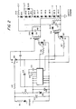
- FIG 2 there is illustrated another embodiment of the high voltage power supply in accordance with the present invention.
- the basic mechanism of Figure 2 is the same as Figure 1 except that the source is 120 VAC at 50/60 Hertz and all the devices are MOS.
Landscapes
- Engineering & Computer Science (AREA)
- Power Engineering (AREA)
- Dc-Dc Converters (AREA)
- Control Of Electrical Variables (AREA)
Claims (4)
Applications Claiming Priority (2)
| Application Number | Priority Date | Filing Date | Title |
|---|---|---|---|
| US517609 | 1983-07-27 | ||
| US06/517,609 US4580206A (en) | 1983-07-27 | 1983-07-27 | Voltage clamp regulator |
Publications (2)
| Publication Number | Publication Date |
|---|---|
| EP0138301A1 EP0138301A1 (de) | 1985-04-24 |
| EP0138301B1 true EP0138301B1 (de) | 1988-09-21 |
Family
ID=24060501
Family Applications (1)
| Application Number | Title | Priority Date | Filing Date |
|---|---|---|---|
| EP84304768A Expired EP0138301B1 (de) | 1983-07-27 | 1984-07-12 | Hochspannungsschaltnetzteil |
Country Status (4)
| Country | Link |
|---|---|
| US (1) | US4580206A (de) |
| EP (1) | EP0138301B1 (de) |
| JP (1) | JPS6049413A (de) |
| DE (1) | DE3474241D1 (de) |
Families Citing this family (3)
| Publication number | Priority date | Publication date | Assignee | Title |
|---|---|---|---|---|
| US5118993A (en) * | 1990-11-23 | 1992-06-02 | Yang Tai Her | Variable voltage regulator |
| US20070195471A1 (en) * | 2006-02-17 | 2007-08-23 | Honeywell International Inc. | Voltage clamp |
| US8847534B2 (en) * | 2010-03-31 | 2014-09-30 | Hitachi Appliances, Inc. | Converter, motor driving module, and refrigerating apparatus |
Family Cites Families (18)
| Publication number | Priority date | Publication date | Assignee | Title |
|---|---|---|---|---|
| US1883613A (en) * | 1931-09-05 | 1932-10-18 | Union Switch & Signal Co | Voltage regulating apparatus |
| US2984780A (en) * | 1955-06-06 | 1961-05-16 | Avien Inc | Reference voltage source |
| US3091729A (en) * | 1959-03-06 | 1963-05-28 | Borg Warner | Static inverter |
| US3063001A (en) * | 1959-04-07 | 1962-11-06 | Hoffman Electronics Corp | Zener diode rectifier and regulator circuits |
| US3328664A (en) * | 1964-05-08 | 1967-06-27 | Allis Chalmers Mfg Co | Transistor reverse current protective circuit |
| US3430127A (en) * | 1966-03-28 | 1969-02-25 | Israel State | Voltage regulator and switching system |
| DE1934223A1 (de) * | 1969-07-05 | 1971-01-21 | Siemens Ag | Schaltungsanordnung zum Erzeugen einer stabilisierten Gleichspannung |
| JPS52543B2 (de) * | 1972-07-10 | 1977-01-08 | ||
| US4162525A (en) * | 1977-03-30 | 1979-07-24 | Hughes Aircraft Company | Power system having an inductive charge effect limiting inverter |
| US4128868A (en) * | 1977-03-30 | 1978-12-05 | Rca Corporation | D-C converter using pulsed resonant circuit |
| JPS5815490B2 (ja) * | 1978-07-06 | 1983-03-25 | 旭化成株式会社 | 耐溶剤性に優れたアクリル樹脂成形材料 |
| US4236198A (en) * | 1977-12-16 | 1980-11-25 | Sony Corporation | Switching regulator |
| JPS56168243A (en) * | 1980-05-28 | 1981-12-24 | Toshiba Corp | Constant-voltage circuit |
| DE3026040C2 (de) * | 1980-07-09 | 1982-05-27 | Siemens AG, 1000 Berlin und 8000 München | Schalter mit in Serie geschalteten MOS-FET |
| JPS57122669A (en) * | 1981-01-23 | 1982-07-30 | Tamura Electric Works Ltd | Switching source |
| DE3128632A1 (de) * | 1981-07-20 | 1983-02-03 | Siemens AG, 1000 Berlin und 8000 München | Ueberspannungsschutzschaltung mit einer zenerdiode |
| JPS5819920A (ja) * | 1981-07-28 | 1983-02-05 | Fujitsu Ltd | 電源装置 |
| US4386311A (en) * | 1981-09-08 | 1983-05-31 | Motorola Inc. | Dual slope pulse width modulation regulator and control system |
-
1983
- 1983-07-27 US US06/517,609 patent/US4580206A/en not_active Expired - Fee Related
-
1984
- 1984-07-12 DE DE8484304768T patent/DE3474241D1/de not_active Expired
- 1984-07-12 EP EP84304768A patent/EP0138301B1/de not_active Expired
- 1984-07-19 JP JP59148721A patent/JPS6049413A/ja active Pending
Also Published As
| Publication number | Publication date |
|---|---|
| US4580206A (en) | 1986-04-01 |
| JPS6049413A (ja) | 1985-03-18 |
| EP0138301A1 (de) | 1985-04-24 |
| DE3474241D1 (en) | 1988-10-27 |
Similar Documents
| Publication | Publication Date | Title |
|---|---|---|
| EP0123030B1 (de) | Schaltnetzteil mit isolierter Rückkopplung | |
| US5963438A (en) | Bi-directional magnetic isolator | |
| US4295083A (en) | Pulsed energy stepping motor power control unit | |
| US4004209A (en) | Wide range power conversion system | |
| EP0367380A2 (de) | Doppelkommutierungsleistungssperrwandler | |
| JPH0527339B2 (de) | ||
| US6362985B1 (en) | Power transmission apparatus and method for power transmission | |
| US4580206A (en) | Voltage clamp regulator | |
| US4974142A (en) | Bootstrap drive for a switch-mode power converter | |
| EP0061744A2 (de) | Transistor-Invertiervorrichtung | |
| US3938015A (en) | SCR motor voltage controller | |
| EP0391679B1 (de) | Oszillatorschaltung | |
| JPH0464207B2 (de) | ||
| EP0061730A2 (de) | Transistor-Wechselrichtereinrichtung | |
| EP0156586B1 (de) | Getaktete Stromversorgung | |
| JPH03872Y2 (de) | ||
| EP0099474B1 (de) | Elektronischer Ansteuerungskreis für eine Entladungslampe | |
| JPS6227030Y2 (de) | ||
| JPS59163724A (ja) | 交流電流の導通・遮断装置 | |
| JP2928945B2 (ja) | 直流電源装置 | |
| JP2872279B2 (ja) | Dc―acインバータ | |
| JPH0681501B2 (ja) | スイッチング回路 | |
| JPH0441739Y2 (de) | ||
| GB2093285A (en) | Battery Charger/Controller | |
| JP2629585B2 (ja) | 突入電流抑制回路 |
Legal Events
| Date | Code | Title | Description |
|---|---|---|---|
| PUAI | Public reference made under article 153(3) epc to a published international application that has entered the european phase |
Free format text: ORIGINAL CODE: 0009012 |
|
| AK | Designated contracting states |
Designated state(s): DE FR GB |
|
| 17P | Request for examination filed |
Effective date: 19850925 |
|
| 17Q | First examination report despatched |
Effective date: 19860821 |
|
| GRAA | (expected) grant |
Free format text: ORIGINAL CODE: 0009210 |
|
| AK | Designated contracting states |
Kind code of ref document: B1 Designated state(s): DE FR GB |
|
| REF | Corresponds to: |
Ref document number: 3474241 Country of ref document: DE Date of ref document: 19881027 |
|
| ET | Fr: translation filed | ||
| PLBE | No opposition filed within time limit |
Free format text: ORIGINAL CODE: 0009261 |
|
| STAA | Information on the status of an ep patent application or granted ep patent |
Free format text: STATUS: NO OPPOSITION FILED WITHIN TIME LIMIT |
|
| 26N | No opposition filed | ||
| PGFP | Annual fee paid to national office [announced via postgrant information from national office to epo] |
Ref country code: GB Payment date: 19920508 Year of fee payment: 9 |
|
| PGFP | Annual fee paid to national office [announced via postgrant information from national office to epo] |
Ref country code: FR Payment date: 19920613 Year of fee payment: 9 |
|
| PGFP | Annual fee paid to national office [announced via postgrant information from national office to epo] |
Ref country code: DE Payment date: 19920702 Year of fee payment: 9 |
|
| PG25 | Lapsed in a contracting state [announced via postgrant information from national office to epo] |
Ref country code: GB Effective date: 19930712 |
|
| GBPC | Gb: european patent ceased through non-payment of renewal fee |
Effective date: 19930712 |
|
| PG25 | Lapsed in a contracting state [announced via postgrant information from national office to epo] |
Ref country code: FR Effective date: 19940331 |
|
| PG25 | Lapsed in a contracting state [announced via postgrant information from national office to epo] |
Ref country code: DE Effective date: 19940401 |
|
| REG | Reference to a national code |
Ref country code: FR Ref legal event code: ST |