EP0138406A2 - Registre à décalage - Google Patents
Registre à décalage Download PDFInfo
- Publication number
- EP0138406A2 EP0138406A2 EP84306388A EP84306388A EP0138406A2 EP 0138406 A2 EP0138406 A2 EP 0138406A2 EP 84306388 A EP84306388 A EP 84306388A EP 84306388 A EP84306388 A EP 84306388A EP 0138406 A2 EP0138406 A2 EP 0138406A2
- Authority
- EP
- European Patent Office
- Prior art keywords
- transistor
- shift register
- circuit
- clock signal
- signal
- Prior art date
- Legal status (The legal status is an assumption and is not a legal conclusion. Google has not performed a legal analysis and makes no representation as to the accuracy of the status listed.)
- Granted
Links
Images



Classifications
-
- G—PHYSICS
- G11—INFORMATION STORAGE
- G11C—STATIC STORES
- G11C19/00—Digital stores in which the information is moved stepwise, e.g. shift registers
-
- G—PHYSICS
- G11—INFORMATION STORAGE
- G11C—STATIC STORES
- G11C19/00—Digital stores in which the information is moved stepwise, e.g. shift registers
- G11C19/02—Digital stores in which the information is moved stepwise, e.g. shift registers using magnetic elements
- G11C19/08—Digital stores in which the information is moved stepwise, e.g. shift registers using magnetic elements using thin films in plane structure
-
- G—PHYSICS
- G11—INFORMATION STORAGE
- G11C—STATIC STORES
- G11C19/00—Digital stores in which the information is moved stepwise, e.g. shift registers
- G11C19/18—Digital stores in which the information is moved stepwise, e.g. shift registers using capacitors as main elements of the stages
- G11C19/182—Digital stores in which the information is moved stepwise, e.g. shift registers using capacitors as main elements of the stages in combination with semiconductor elements, e.g. bipolar transistors, diodes
- G11C19/184—Digital stores in which the information is moved stepwise, e.g. shift registers using capacitors as main elements of the stages in combination with semiconductor elements, e.g. bipolar transistors, diodes with field-effect transistors, e.g. MOS-FET
-
- G—PHYSICS
- G11—INFORMATION STORAGE
- G11C—STATIC STORES
- G11C19/00—Digital stores in which the information is moved stepwise, e.g. shift registers
- G11C19/28—Digital stores in which the information is moved stepwise, e.g. shift registers using semiconductor elements
Definitions
- the present invention relates to a shift register, and more particularly to a MIS dynamic shift register which can be composed by using a small number of circuit elements.
- a In a MIS dynamic memory device for/so called auto-refresh operation for refreshing data stored (address) in each memory cell is effected by memorizing the number/ of a word line to be refreshed in the memory device, and by incrementing the number of the word line and refreshing the memory cells connected to each word line.
- a memory device which comprises a shift register disposed parallel: to a row decoder and in which a selecting signal for a word line to be refreshed is generated . using an output signal of the shift register, thereby sequentially selecting a word line to be refreshed.
- the shift register used in such a memory device is characterized in that, among all the bits thereof, the output of only one bit is "1" and the outputs of other bits are all "0". By using the output e of/one bit which is "1", only one target word line is selected. It is also necessary that the width of one circuit stage on a semiconductor substrate of such a shift register be not larger than the pitch length of the word lines. Generally, since the pitch length of the word lines is very narrow, it is necessary that the structure of each circuit stage of the shift register be very simple and the number of circuit components used therein be small.
- each circuit stage has a very complex circuit structure and a large number of circuit components. Therefore, the circuit width of each circuit stage on a semiconductor device is such a relatively large, and it is impossible to use / shift register in the above-mentioned memory device.
- the present invention adopts an idea of constituting each circuit stage in a MIS dynamic-type shift register by using three MIS transistors as base components.
- An embodiment of the present invention can simplify the circuit structure of each circuit stage and decrease the number of circuit components used in each circuit stage, thereby decreasing the width of the space occupied by each circuit stage on a semiconductor substrate.
- a shift register having a plurality of circuit stages connected in cascade and receiving first and second clock signals different in phase from each other for driving the shift register, each of the circuit stages comprising: a first transistor operatively connected to receive an input signal and the first clock signal for transferring the input signal in response to the first clock signal; a second transistor having a gate operatively connected to receive the input signal, a source and a drain, one of the source and drain receiving the second clock signal, the second transistor providing an output signal at the other of the source and drain in response to the input signal and the second clock signal; and a reset means for resetting the input signal applied to the first transistor in response to the output signal, the output signal of the present circuit stage providing the input signal applied to the first transistor of the succeeding stage.
- Figure 1 illustrates a dynamic memory device possibly a ring counter type shift register, wherein a shift register/is used to sequentially designate a word line connected to memory cells for the purpose of / refresh operation.
- the memory device of Fig. 1 comprises a memory cell array MCA having a plurality of memory cells MC each being connected to a bit line BL and a word line WL, a column decoder CD, a word decoder WD, and the above-mentioned shift register SR.
- the word decoder comprises a NOR gate NG for decoding address signals and an electronic switch SW for every word line WL.
- an access operation such as a readout operation or write-in operation is effected in a state in which the switch SW is positioned so as to connect the output of the NOR gate NG to the corresponding word line WL.
- the word line WL is selected by a decoded signal, i.e., the output signal of the NOR gate NG, and the bit line BL is selected by the column decoder CD.
- the memory cell MC is selected and the access thereto is performed in a known manner.
- the switch SW is controlled by/refresh enable signal RFE of, for example, a high potential level so as to connect each of the output terminals of the shift register SR to the corresponding word lines.
- RFE freshness enable signal
- the shift a register SR shifts/data "1" cyclically, and selects a word line sequentially, thereby refreshing memory cells connected to each word line.
- Figure 2 illustrates a structure of a shift register as an embodiment of the present invention used, for example, in the memory device of Fig. 1.
- the circuit portion surrounded by a dot-dash line constitutes a circuit of one stage of the shift register, and comprises three MIS transistors Q 4 , Q 5 , and Q 6 , and one capacitor C 2 .
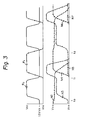
- the shift register of Fig. 2 is controlled by two kinds of clock pulses ⁇ 0 and ⁇ 1 , and these clock pulses ⁇ 0 and ⁇ 1 have phases mutually different, for example, by 180°, as shown in Fig. 3.
- the clock pulse ⁇ 1 has an amplitude extending between power supply voltages V SS and V CC .
- the voltage of a low level portion of the clock pulse ⁇ 0 is within the range of Vth to 2Vth and is preferably 1.5 Vth, although the voltage of a high level portion thereof is V CC ; where Vth is a threshold that of voltage of the M IS transistors, for example/Q 4 .
- the potential of the clock pulse ⁇ 0 is at a low level, but since the low level potential of the clock pulse ⁇ 0 is 1.5 Vth as mentioned before, when the potential of the node N2 becomes lower than 1/2 Vth, the transistor Q 4 is turned on, thereby pulling down the potential of the node N3 rapidly. In this way, transmission of the high level potential from the node N2 to node N4 is effected, and, similarly, the high level potential is sequentially transmitted through each circuit stage.
- the capacitor C 2 is provided so as to decrease the voltage loss caused when electric charges are transmitted from one stage to a succeeding stages by rendering the capacitance of the output node N4 sufficiently larger than that of the input circuit, i.e. the node N5 of the succeeding stage.
- the low level voltage of the clock pulse ⁇ 0 is 1.5 Vth
- the potential of the node N4 is at a high level and the clock pulse ⁇ 0 is at a low level, i.e., 1.5 Vth
- the potential of the node N5 of the next stage becomes 0.5 Vth and it of the succeeding stage in is possible to keep a- transistor Q 8 / a cut-off state. Therefore, it is possible to maintain the potential of a node N6 at a low level, i.e., V SS .
- the low level potential of the clock pulse ⁇ 0 is equal to or larger than 2 Vth, the potential of the node N6 disadvantageously rises to a value equal to or larger than V SS in the response to/rise or fall of the clock pulse ⁇ 1 . It is necessary that the low level voltage of the clock pulse ⁇ 0 is higher than Vth and lower than 2 Vth. Considering the variations in characteristics of each MIS transistor, it is preferable that the low level voltage of the clock pulse ⁇ 0 is a value near 1.5 Vth.
- Figure 4 illustrates a circuit of one stage of a shift register as another embodiment of the present invention.
- the circuit of Fig. 4 differs from that of Fig. 2 in that a transistor Q 4 ' is connected in parallel to the input transfer gate transistor Q 4 , a voltage V B having a voltage of approximately 1.5 Vth is applied to the gate of the transistor Q4', and the clock pulse ⁇ 0 in Fig. 2 is replaced by a clock pulse ⁇ 0 '.
- the low level voltage of the clock pulse ⁇ 0 ' is V SS which is the same as that of the clock pulse ⁇ 1 , and the clock pulse ⁇ 0 ' has the same waveform as that of a pulse formed by shifting the phase of the clock pulse ⁇ 1 for example. by 180°,/
- the other portions of Fig. 4 are the same as those of the circuit of Fig. 2 and are designated by the same reference symbols.
- the parallel circuit of the transistors Q 4 and Q 4 ' effects the same operation as that of the transistor Q 4 of Fig. 2. That is, when the clock pulse ⁇ 0 ' is low, the transistor Q 4 is turned off and the nodes N2 and N3 are connected only via the transistor Q 4 '. Since the voltage V B of 1.5 Vth is applied to the gate of the transistor Q 4 ', the transistor Q 4 1 becomes equivalent to the transistor Q 4 when the clock pulse ⁇ 0 in the circuit of Fig. 2 is in a low potential level, i.e., 1.5 Vth.
- Figure 5 illustrates a circuit of one stage of a shift register as still other embodiment of the present invention.
- the circuit of Fig. 5 further comprises transistors Q6' and Q 6 " connected to the transistor Q 6 in the circuit of Fig. 2.
- the transistors Q 6 and Q 6 " are mutually cross-coupled at the gates and the drains, and a signal from the output node N6 of the succeeding stage is input to the drain of the transistor Q 6 ", i.e., a node N4' via the transistor Q 6 '.
- the other portions are the same as those of the circuit of Fig. 2 and are designated by the same reference symbols.
- a high level voltage of, for example, the node N4 is transmitted to the succeeding stage circuit, and when the output node N6 of the succeeding circuit becomes high, the potential of the node N4', i.e., the gate of the transistor Q 6 becomes high, thereby clamping the potential of the node N4 to V SS .
- the potential of the succeeding output node N6 becomes low after the high level voltage of the succeeding output node N6 is transmitted to a further succeeding stage, the potential of the node N4 is low and, thus, the potential of the node N4' is still high, so that the potential of the node N4 is always clamped to the voltage V SS by the transistor Q 6 .
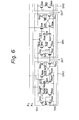
- FIG. 6 illustrates a shift register as still another embodiment of the present invention.
- Each stage of the shift register for example, a stage SRl,comprises eleven MIS transistors Q 101 , Q 102 , ---, Q 111 .
- the transistor Q 110 is a depletion type load transistor.
- the transistors Q 101 , ---, Q 104 constitute an input circuit and a first reset means for resetting an input (a node N 12) portion/of a transistor Q 105 .
- the transistors Q 106 and Q 107 constitute a second reset means which resets an output portion/of the transistor Q 105 .
- the transistors Q 109 , Q 110 and Q 111 constitute a latch circuit which is driven by the output signal of a transistor Q 108 .
- Clock pulses ⁇ 2 and ⁇ 3 are pulses having a phase difference of, for example, 180°.
- the high potential level of both clock pulses ⁇ 2 and ⁇ 3 is V CC
- the low potential level of both clock gulses ⁇ 2 and ⁇ 3 is V SS.
- the potential of the clock pulse ⁇ 3 changes from high to low.
- a current flows from the node N05 to a clock line ⁇ 3 via the transistor Q 008 , and the potential of the node N05 changes from high to low, i.e., the output signal of the circuit stage SRO becomes "0".
- the transistor Q 011 is turned off, and the potential of a node N06 changes from low to high.
- the potential of the clock pulse ⁇ 2 changes from low to high, a high level signal is transmitted from a node N12 to a node N13 via the turned on transistor Q 105 , so that the potential of the node N13 becomes high. Thereafter, the clock pulse ⁇ 2 again changes from high to low.
- the clock pulse ⁇ 3 changes from low to high. Since the potential of the node N13 is high, the potential of the node N15 is pulled up to high via the turned on transistor Q108 , and the output data of the circuit stage SR1 becomes "1". When the potential of the node N15 becomes high, the transis- tor Q 101 is turned on, and the potential of a node Nll becomes high. Thereby, the transistor Q104 is turned on, and the node N12 is reset from high to low.
- the transistor Q 007 is turned on.
- the transistor Q 006 is also turned on because of the high potential level of the clock pulse ⁇ 3 . Therefore, the potential of the node N03 is reset to low, and the transmission of data "1" from the circuit stage SRO to the circuit stage SR1 is performed (completed).
- the present shift register for example a invention, it is possible to constitute a/ring counter type shift register by using a very simple circuit structure, and to considerablyreduce the width occupied by , each circuit stage on a semiconductor substrate. Therefore, it becomes very advantageous to dispose the shift register parallel to a decoder as mentioned before.
Landscapes
- Engineering & Computer Science (AREA)
- Microelectronics & Electronic Packaging (AREA)
- Power Engineering (AREA)
- Shift Register Type Memory (AREA)
Applications Claiming Priority (2)
| Application Number | Priority Date | Filing Date | Title |
|---|---|---|---|
| JP172096/83 | 1983-09-20 | ||
| JP58172096A JPS6066396A (ja) | 1983-09-20 | 1983-09-20 | シフトレジスタ |
Publications (3)
| Publication Number | Publication Date |
|---|---|
| EP0138406A2 true EP0138406A2 (fr) | 1985-04-24 |
| EP0138406A3 EP0138406A3 (en) | 1987-06-03 |
| EP0138406B1 EP0138406B1 (fr) | 1991-11-13 |
Family
ID=15935462
Family Applications (1)
| Application Number | Title | Priority Date | Filing Date |
|---|---|---|---|
| EP84306388A Expired EP0138406B1 (fr) | 1983-09-20 | 1984-09-19 | Registre à décalage |
Country Status (5)
| Country | Link |
|---|---|
| US (1) | US4679214A (fr) |
| EP (1) | EP0138406B1 (fr) |
| JP (1) | JPS6066396A (fr) |
| KR (1) | KR890002961B1 (fr) |
| DE (1) | DE3485260D1 (fr) |
Cited By (2)
| Publication number | Priority date | Publication date | Assignee | Title |
|---|---|---|---|---|
| EP0202912A3 (fr) * | 1985-05-20 | 1989-05-24 | Fujitsu Limited | Dispositif de mémoire semi-conductrice en forme de registre à décalage alimenté par un signal d'horloge à deux phases |
| EP0768674A1 (fr) * | 1995-10-16 | 1997-04-16 | STMicroelectronics S.A. | Procédé d'initialisation d'un registre à décalage et registre associé |
Families Citing this family (9)
| Publication number | Priority date | Publication date | Assignee | Title |
|---|---|---|---|---|
| US4902919A (en) * | 1988-09-26 | 1990-02-20 | Motorola, Inc. | Inverting latching bootstrap driver with Vdd *2 booting |
| US4897816A (en) * | 1989-04-03 | 1990-01-30 | Tektronix, Inc. | Serial dynamic memory shift register |
| JPH05196659A (ja) * | 1991-11-08 | 1993-08-06 | Yamaha Corp | チョッパ型比較器 |
| US5517542A (en) * | 1995-03-06 | 1996-05-14 | Thomson Consumer Electronics, S.A. | Shift register with a transistor operating in a low duty cycle |
| GB2343310A (en) * | 1998-10-27 | 2000-05-03 | Sharp Kk | Clock pulse generator for LCD |
| GB2361121A (en) | 2000-04-04 | 2001-10-10 | Sharp Kk | A CMOS LCD scan pulse generating chain comprising static latches |
| KR100551734B1 (ko) * | 2003-05-21 | 2006-02-13 | 비오이 하이디스 테크놀로지 주식회사 | 액정구동장치의 행구동회로에 사용되는 쉬프트 레지스터 |
| TWI386904B (zh) * | 2008-05-12 | 2013-02-21 | Chimei Innolux Corp | 平面顯示器 |
| US10102892B1 (en) | 2017-06-01 | 2018-10-16 | Intel Corporation | RAM-based shift register with embedded addressing |
Family Cites Families (5)
| Publication number | Priority date | Publication date | Assignee | Title |
|---|---|---|---|---|
| US3683203A (en) * | 1969-09-08 | 1972-08-08 | Gen Instrument Corp | Electronic shift register system |
| US3601637A (en) * | 1970-06-25 | 1971-08-24 | North American Rockwell | Minor clock generator using major clock signals |
| JPS54161288A (en) * | 1978-06-12 | 1979-12-20 | Hitachi Ltd | Semiconductor device |
| US4341960A (en) * | 1980-02-21 | 1982-07-27 | General Instrument Corporation | I2 L Static shift register |
| JPS57176596A (en) * | 1981-04-20 | 1982-10-29 | Sanyo Electric Co Ltd | Shift register |
-
1983
- 1983-09-20 JP JP58172096A patent/JPS6066396A/ja active Granted
-
1984
- 1984-09-07 KR KR1019840005491A patent/KR890002961B1/ko not_active Expired
- 1984-09-10 US US06/648,506 patent/US4679214A/en not_active Expired - Fee Related
- 1984-09-19 DE DE8484306388T patent/DE3485260D1/de not_active Expired - Lifetime
- 1984-09-19 EP EP84306388A patent/EP0138406B1/fr not_active Expired
Cited By (4)
| Publication number | Priority date | Publication date | Assignee | Title |
|---|---|---|---|---|
| EP0202912A3 (fr) * | 1985-05-20 | 1989-05-24 | Fujitsu Limited | Dispositif de mémoire semi-conductrice en forme de registre à décalage alimenté par un signal d'horloge à deux phases |
| EP0768674A1 (fr) * | 1995-10-16 | 1997-04-16 | STMicroelectronics S.A. | Procédé d'initialisation d'un registre à décalage et registre associé |
| FR2739967A1 (fr) * | 1995-10-16 | 1997-04-18 | Sgs Thomson Microelectronics | Procede d'initialisaiton d'un registre a decalage et registre associe |
| US5778037A (en) * | 1995-10-16 | 1998-07-07 | Sgs-Thomson Microelectronics S.A. | Method for the resetting of a shift register and associated register |
Also Published As
| Publication number | Publication date |
|---|---|
| EP0138406B1 (fr) | 1991-11-13 |
| KR850002641A (ko) | 1985-05-15 |
| EP0138406A3 (en) | 1987-06-03 |
| DE3485260D1 (de) | 1991-12-19 |
| JPS6066396A (ja) | 1985-04-16 |
| KR890002961B1 (ko) | 1989-08-14 |
| JPH036600B2 (fr) | 1991-01-30 |
| US4679214A (en) | 1987-07-07 |
Similar Documents
| Publication | Publication Date | Title |
|---|---|---|
| US4161040A (en) | Data-in amplifier for an MISFET memory device having a clamped output except during the write operation | |
| KR940001493B1 (ko) | 반도체 메모리 | |
| EP0071245B1 (fr) | Dispositif de mémoire semi-conductrice | |
| CA1224567A (fr) | Memoire a semiconducteur a structure multiniveau | |
| EP0395881A1 (fr) | Circuit de suralimentation de tension pour mémoires dynamiques | |
| US4514829A (en) | Word line decoder and driver circuits for high density semiconductor memory | |
| US4104733A (en) | Address selecting circuitry for semiconductor memory device | |
| EP0138406A2 (fr) | Registre à décalage | |
| US5708599A (en) | Semiconductor memory device capable of reducing power consumption | |
| JPS61175994A (ja) | メモリのデコ−ド・ドライブ回路 | |
| US4281401A (en) | Semiconductor read/write memory array having high speed serial shift register access | |
| US4990800A (en) | Mode selector for use in semiconductor memory device | |
| EP0085436B1 (fr) | Circuits tampons | |
| US4797573A (en) | Output circuit with improved timing control circuit | |
| US4831590A (en) | Semiconductor memory including an output latch having hysteresis characteristics | |
| US4602355A (en) | Memory circuit with noise preventing means for word lines | |
| EP0168246A2 (fr) | Circuit actif de tirage | |
| KR100253603B1 (ko) | 래치회로 및 래치회로를 포함하는 메모리시스템 | |
| US4682048A (en) | Output circuit with improved timing control circuit | |
| US4484312A (en) | Dynamic random access memory device | |
| US4209851A (en) | Semiconductor memory cell with clocked voltage supply from data lines | |
| EP0293808B1 (fr) | Circuit intégré à semi-conducteurs | |
| EP0148364B1 (fr) | Générateur de signal de référence temporelle | |
| US6310795B1 (en) | Semiconductor memory device with data retention characteristic of improved stability | |
| US4870620A (en) | Dynamic random access memory device with internal refresh |
Legal Events
| Date | Code | Title | Description |
|---|---|---|---|
| PUAI | Public reference made under article 153(3) epc to a published international application that has entered the european phase |
Free format text: ORIGINAL CODE: 0009012 |
|
| AK | Designated contracting states |
Designated state(s): DE FR GB |
|
| PUAL | Search report despatched |
Free format text: ORIGINAL CODE: 0009013 |
|
| AK | Designated contracting states |
Kind code of ref document: A3 Designated state(s): DE FR GB |
|
| PUAF | Information related to the publication of a search report (a3 document) modified or deleted |
Free format text: ORIGINAL CODE: 0009199SEPU |
|
| D17D | Deferred search report published (deleted) | ||
| PUAL | Search report despatched |
Free format text: ORIGINAL CODE: 0009013 |
|
| AK | Designated contracting states |
Kind code of ref document: A3 Designated state(s): DE FR GB |
|
| 17P | Request for examination filed |
Effective date: 19880629 |
|
| 17Q | First examination report despatched |
Effective date: 19891019 |
|
| GRAA | (expected) grant |
Free format text: ORIGINAL CODE: 0009210 |
|
| AK | Designated contracting states |
Kind code of ref document: B1 Designated state(s): DE FR GB |
|
| PGFP | Annual fee paid to national office [announced via postgrant information from national office to epo] |
Ref country code: FR Payment date: 19911119 Year of fee payment: 9 |
|
| REF | Corresponds to: |
Ref document number: 3485260 Country of ref document: DE Date of ref document: 19911219 |
|
| ET | Fr: translation filed | ||
| PLBE | No opposition filed within time limit |
Free format text: ORIGINAL CODE: 0009261 |
|
| STAA | Information on the status of an ep patent application or granted ep patent |
Free format text: STATUS: NO OPPOSITION FILED WITHIN TIME LIMIT |
|
| PG25 | Lapsed in a contracting state [announced via postgrant information from national office to epo] |
Ref country code: GB Effective date: 19920919 |
|
| 26N | No opposition filed | ||
| GBPC | Gb: european patent ceased through non-payment of renewal fee |
Effective date: 19920919 |
|
| PG25 | Lapsed in a contracting state [announced via postgrant information from national office to epo] |
Ref country code: DE Effective date: 19930602 |
|
| PG25 | Lapsed in a contracting state [announced via postgrant information from national office to epo] |
Ref country code: FR Free format text: LAPSE BECAUSE OF NON-PAYMENT OF DUE FEES Effective date: 19940531 |
|
| REG | Reference to a national code |
Ref country code: FR Ref legal event code: ST |