EP0138453B1 - Montage d'interface pour un système téléphonique ou analogue - Google Patents
Montage d'interface pour un système téléphonique ou analogue Download PDFInfo
- Publication number
- EP0138453B1 EP0138453B1 EP84306549A EP84306549A EP0138453B1 EP 0138453 B1 EP0138453 B1 EP 0138453B1 EP 84306549 A EP84306549 A EP 84306549A EP 84306549 A EP84306549 A EP 84306549A EP 0138453 B1 EP0138453 B1 EP 0138453B1
- Authority
- EP
- European Patent Office
- Prior art keywords
- bus
- parallel
- serial
- digital
- connection memory
- Prior art date
- Legal status (The legal status is an assumption and is not a legal conclusion. Google has not performed a legal analysis and makes no representation as to the accuracy of the status listed.)
- Expired
Links
- 230000015654 memory Effects 0.000 claims abstract description 36
- 230000006870 function Effects 0.000 claims description 5
- 230000001131 transforming effect Effects 0.000 claims description 4
- 238000013500 data storage Methods 0.000 claims 1
- 238000009432 framing Methods 0.000 description 6
- 238000000034 method Methods 0.000 description 3
- 238000010586 diagram Methods 0.000 description 2
- WABPQHHGFIMREM-IGMARMGPSA-N lead-207 Chemical compound [207Pb] WABPQHHGFIMREM-IGMARMGPSA-N 0.000 description 2
- 230000009977 dual effect Effects 0.000 description 1
- 238000002592 echocardiography Methods 0.000 description 1
- 239000000284 extract Substances 0.000 description 1
- WABPQHHGFIMREM-OUBTZVSYSA-N lead-208 Chemical compound [208Pb] WABPQHHGFIMREM-OUBTZVSYSA-N 0.000 description 1
- WABPQHHGFIMREM-NJFSPNSNSA-N lead-209 Chemical compound [209Pb] WABPQHHGFIMREM-NJFSPNSNSA-N 0.000 description 1
- 230000011664 signaling Effects 0.000 description 1
Images


Classifications
-
- H—ELECTRICITY
- H04—ELECTRIC COMMUNICATION TECHNIQUE
- H04Q—SELECTING
- H04Q11/00—Selecting arrangements for multiplex systems
- H04Q11/04—Selecting arrangements for multiplex systems for time-division multiplexing
Definitions
- the present invention relates generally to processing digital signals appearing on a bus, and more particularly to a parallel bus arrangement for allowing this to happen in an easily reconfigurable fashion in a telephone system.
- time division multiplexing It is also common to multiplex a plurality of such digital signals onto a single serial bus, via a technique referred to as time division multiplexing. Two of the more common methods of doing this are to multiplex either 24 or 32 channels onto a single serial bus.
- DTMF dual tone multi-frequency
- a digital telephone system including, inter alia, a digital echo suppressor which can process eight channels of a digital telephone bus under the control of a centralized control device.
- the digital echo suppressor operates directly on a pulse code modulated signal, extracts all information regarding the presence of speech or data signals from the PCM stream, and blocks the echo in one direction.
- a de-centralized control system is employed to control the accessing of the bus by the appropriate signal processing circuits.
- This de-centralized accessing is achieved by having one connection memory associated with each signal processing circuit.
- the connection memories are all responsive both to a common clock signal, and to a common framing signal. Accordingly, each individual processing circuit has its access to the TDM bus controlled by its own dedicated connection memory. If a processing circuit is to be added to the bus (or an existing circuit altered) then, in most cases, only the connection memory associated with that particular processing circuit need be adjusted.
- the present invention is an interface means for applying information from a channel of a first digital bus to at least one processing circuit and for returning the information, after processing, to a respective channel, the means characterized by: converter means for transforming the digital data on said first bus to digital data on a second digital bus; circuit means for selectively accessing the second bus, under the control of a connection memory means; the connection memory means responsive to timing signals for controlling the access of the circuit means to the second bus such that the circuit means accesses the second bus at the appropriate time to receive the digital information from a selected channel on the second bus, and also accesses the second bus at the appropriate time to transmit the digital information to a selected channel on the second bus.
- the present invention is an interface device for applying information from a channel of a serial digital bus to at least one processing circuit and for returning the information, after processing, to a respective channel, the device characterized by; serial to parallel converter device for transforming the serial bits from the serial bus to parallel bits on a parallel digital bus; circuitry for selectively accessing the parallel bus, under the control of a connection memory; the connection memory responsive to timing signals for controlling the access of the circuitry to the parallel bus such that the circuitry accesses the parallel bus at the appropriate time to receive the digital information from a selected channel on the parallel bus, corresponding to the channel on the serial bus, and also accesses the parallel bus at the appropriate time to transmit the digital information to a selected channel on the parallel bus, corresponding to the channel on the serial bus.
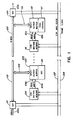
- Figure 1 depicts one embodiment of the present invention in the form of interface circuit 105 (note: circuit 105 includes everything shown in Figure 1 except serial bus 100a, serial bus 100b, AGC 119, and echo control 117).
- Serial bus 100a is applied to serial to parallel converter 101 which has as its output 8 bit wide parallel bus 102.
- Serial bus 100a has 32 channels, each of ten bits and has a frame period of 125 micro-seconds.
- Parallel bus 102 has 320 channels, each eight bits wide and has a frame period of 125 micro-seconds (note that bus 102 could have been ten bits wide, but for the present application only an eight bit wide bus is needed).
- AGC (automatic gain control) circuit 119 is connected to bus 102 via input/output buffer 103 and eight-bit bus 104.
- Connection memory 106 controls the connection of buffer 103, and consequently AGC 119, to bus 102.
- Connection memory 106 is responsive both to a 2.56 MHz clock signal on lead 107 and to framing pulse (occurring once every 125 micro-seconds) on lead 108.
- the function of connection memory 106 is to control the accessing of bus 102 by buffer 103.
- connection memory 106 controls when buffer 103 reads data from bus 102 or writes data onto bus 102. This control is via read control lead 109a and write control lead 109b.
- Echo control circuit 117 is controlled in an analogous manner to AGC circuit 119.
- Echo control circuit 117 is connected to bus 102 via input/ output buffer 113 and eight-bit bus 114.
- Connection memmory 116 controls the connection of buffer 113 and consequently echo control circuit 117 to bus 102.
- Connection memory 116 is repon- sive both to a 2.56 MHz clock signal on lead 107 and to a framing pulse (occurring once every 125 micro-seconds) on lead 108.
- the function of connection memory 116 is to control the accessing of bus 102 by buffer 113.
- connection memory 116 controls when buffer 113 reads data from bus 102 or writes data onto bus 102. This control is via read control lead 121a and write control lead 121b.
- connection memories 106 and 116 function as follows. They count the clock pulses appearing on lead 107 and when they reach a preset count they enable the appropriate control lead. They are reset back to an initial state by the framing pulse appearing on lead 108 (once every 320 cycles of the clock waveform on lead 107).
- parallel bus 102 can be applied to the input of a parallel to serial converter 124.
- Converter 124 produces a serial output on serial bus 100b of 32 channels per frame, each channel comprising ten bits (eight of which are derived from bus 102).
- Serial buses 100a and 100b are referred to collectively as bus 100.
- Figure 2 depicts a second and preferred embodiment of the present invention in the form of interface circuit 205 (note: circuit 205 includes everything shown in Figure 2 except, bus 200a, bus 220b, AGC 219, and echo control 217).
- circuit 205 includes everything shown in Figure 2 except, bus 200a, bus 220b, AGC 219, and echo control 217).
- the major difference in the Figure 2 embodiment is that two parallel buses, 202a and 202b are used instead of the single bus 102 (in Figure 1).
- the use of the two parallel buses 202a and 202b results in a doubling of the channel capacity which now becomes 640 channels in the Figure 2 embodiment.
- buses 202a and 202b are both bi-directional, and each consists of eight leads.
- Serial bus 200a is applied to serial to parallel converter 201 which has as its output eightbitwide parallel bus 202a.
- Serial bus 200a has 32 channels, each of ten bits and has frame period of 125 micro-seconds.
- Parallel bus 202a has 320 channels, each eight bits wide and has a frame period of 125 micro-seconds.
- Parallel bus 202b is also an eight bit wide bus, having 320 channels, each of eight bits and has a frame period of 125 micro-seconds.
- Bus 202b is applied to parallel to serial converter 224 which produces a serial output on serial bus 200b of 32 channels per frame, each channel comprising ten bits (eight of which are derived from bus 202b).
- AGC (automatic gain control) circuit 219 is connected to buses 202a and 202b via input/output buffer 203 and eight bit buses 204a and 204b.
- Port address lead 226 determines which port of buffer 203 is to handle data (i.e. to read data from or write data onto either bus 204a or 204b).
- Read control lead 209 and write control lead 209b determine, of course, whether or not the operation will be a read (receive) or a write (transmit).
- buffer 203 can operate in any one of the following modes: a) read from bus 202a (via bus 204a) and write onto bus 202a (via bus 204a); b) read from bus 202a (via bus 204a) and write onto bus 202b (via bus 204b); c) read from bus 202b (via bus 204b) and write onto bus 202b (via bus 204b); and d) read from bus 202b (via bus 204b) and write onto bus 202a (via bus 204a).
- Connection memory 206 controls the connection of buffer 203 and consequently AGC 219 to bus 202a or bus 202b.
- Connection memory 206 is responsive both to a 2.56 MHz clock signal on lead 207 and to a framing pulse (occurring once every 125 micro-seconds) on lead 208.
- the function of connection memory 206 is to control the accessing of bus 202a and 202b by buffer 203.
- connection memory 206 controls (via read and write control leads 209a and 209) when buffer 203 either reads data from bus 202a or 202b, or writes data onto bus 202a or 202b; connection memory 206 also controls (via port address lead 226) which bus (i.e. 202a or 202b) will be read from or written to.
- Echo control circuit 217 is controlled in an analogous manner to AGC circuit 219. Echo control circuit 217 is connected to buses 202a and 202b via input/output buffer 213 and eight bit buses 214a and 214b. Connection memory 216 controls the connection of buffer 213 via read control lead 221, write control lead 221 b, and port address lead 227. Memory 216 is responsive both to a 2.56 MHz clock signal on lead 207 and to a framing pulse (occurring once every 125 micro-seconds) on lead 108.
- connection memories 206 and 216 are analogous to the functioning of memory 106 in Figure 1. The sole difference is existence of port address leads 226 and 227 to determine which bus (i.e. bus 202a or 202b) is to be accessed.
- Figure 3 depicts yet another embodiment, interface circuit 205a, similar to Figure 2, but additionally including a bus 230 and a bus interface device 231.
- bus 230 and bus interface device 231 are to enable the contents of connection memory 206 to be modified by signal on bus 230.
- the signals on bus 230 are applied to connection memory 206 via bus interface device 231, so as to alter the contents stored in connection memory 206 and to consequently change the timeslot during which AGC 219 accesses bus 202a on bus 202b.
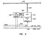
- Figure 4 depicts a simplified embodiment for an asynchronous application of a serial to parallel converter.
- the circuit of Figure 1 was described as 32 channels on bus 100a and 320 channels on bus 102. But suppose that bus 100a has 24 channels and bus 102 still has 320 channels (all in a 125 micro-second frame); some form of synchronization between the two buses (100a and 102) is required.
- Connection memory 250 controls the timing of the operations of serial to parallel converter 253 and RAM 251 so as to put the data on bus 102 at an appropriate time. Data is stored in RAM (random access memory) 251 until it is needed on bus 102. Data is transferred to bus 102 via bus 252. Read lead 254 controls the reading of RAM 251 and consequently the transmitting of digital data from RAM 251 to bus 102. Write lead 256 controls the writing (i.e. receiving) of RAM 251 with digital data from serial to parallel converter 253. Connection memory 250 is responsive to timing signals on leads 107 and 108. The remainder of the circuit (not shown) connected to bus 102 would be as per Figure 1.
Landscapes
- Engineering & Computer Science (AREA)
- Computer Networks & Wireless Communication (AREA)
- Time-Division Multiplex Systems (AREA)
- Communication Control (AREA)
- Telephone Function (AREA)
- Paper (AREA)
- Electrochromic Elements, Electrophoresis, Or Variable Reflection Or Absorption Elements (AREA)
- Complex Calculations (AREA)
- Small-Scale Networks (AREA)
Claims (8)
Priority Applications (1)
| Application Number | Priority Date | Filing Date | Title |
|---|---|---|---|
| AT84306549T ATE28544T1 (de) | 1983-10-11 | 1984-09-26 | Schnittstellenanordnung fuer ein fernsprechsystem oder aehnliches. |
Applications Claiming Priority (2)
| Application Number | Priority Date | Filing Date | Title |
|---|---|---|---|
| CA000438741A CA1221766A (fr) | 1983-10-11 | 1983-10-11 | Interface pour reseaux telephoniques ou leurs analogues |
| CA438741 | 1983-10-11 |
Publications (3)
| Publication Number | Publication Date |
|---|---|
| EP0138453A2 EP0138453A2 (fr) | 1985-04-24 |
| EP0138453A3 EP0138453A3 (en) | 1985-05-29 |
| EP0138453B1 true EP0138453B1 (fr) | 1987-07-22 |
Family
ID=4126253
Family Applications (1)
| Application Number | Title | Priority Date | Filing Date |
|---|---|---|---|
| EP84306549A Expired EP0138453B1 (fr) | 1983-10-11 | 1984-09-26 | Montage d'interface pour un système téléphonique ou analogue |
Country Status (5)
| Country | Link |
|---|---|
| EP (1) | EP0138453B1 (fr) |
| JP (1) | JPS6096948A (fr) |
| AT (1) | ATE28544T1 (fr) |
| CA (1) | CA1221766A (fr) |
| DE (1) | DE3464998D1 (fr) |
Families Citing this family (3)
| Publication number | Priority date | Publication date | Assignee | Title |
|---|---|---|---|---|
| JPS60240294A (ja) * | 1984-05-07 | 1985-11-29 | デイ−・エイ・ヴイ・アイ・デイ−・システムズ・インコ−ポレ−テツド | デジタルpbxスイツチ |
| US4975903A (en) * | 1984-05-07 | 1990-12-04 | David Systems, Inc. | Digital timeslot and signaling bus in a digital PBX switch |
| AU649747B2 (en) * | 1990-11-30 | 1994-06-02 | Telstra Corporation Limited | A telecommunications data accessing device |
Family Cites Families (3)
| Publication number | Priority date | Publication date | Assignee | Title |
|---|---|---|---|---|
| FR2305907A1 (fr) * | 1975-03-27 | 1976-10-22 | Materiel Telephonique | Dispositif de controle destine a un reseau de commutation pour voies multiplexees dans le temps |
| AU537749B2 (en) * | 1980-02-20 | 1984-07-12 | Gec Plessey Telecommunications Limited | Digital telephone exchange with fast control signal processor. |
| US4390982A (en) * | 1981-01-14 | 1983-06-28 | International Telephone And Telegraph Corporation | Digital PBX system |
-
1983
- 1983-10-11 CA CA000438741A patent/CA1221766A/fr not_active Expired
-
1984
- 1984-09-26 EP EP84306549A patent/EP0138453B1/fr not_active Expired
- 1984-09-26 DE DE8484306549T patent/DE3464998D1/de not_active Expired
- 1984-09-26 AT AT84306549T patent/ATE28544T1/de not_active IP Right Cessation
- 1984-10-09 JP JP59210609A patent/JPS6096948A/ja active Pending
Also Published As
| Publication number | Publication date |
|---|---|
| EP0138453A3 (en) | 1985-05-29 |
| EP0138453A2 (fr) | 1985-04-24 |
| ATE28544T1 (de) | 1987-08-15 |
| CA1221766A (fr) | 1987-05-12 |
| DE3464998D1 (en) | 1987-08-27 |
| JPS6096948A (ja) | 1985-05-30 |
Similar Documents
| Publication | Publication Date | Title |
|---|---|---|
| CA1203876A (fr) | Unite de controle peripherique pour systeme telephonique numerique | |
| US3984643A (en) | Method and apparatus for establishing a plurality of simultaneous conferences in a PCM switching system | |
| US4574375A (en) | Interface arrangement for a telephone system or the like | |
| US4048447A (en) | PCM-TASI signal transmission system | |
| CA1221766A (fr) | Interface pour reseaux telephoniques ou leurs analogues | |
| US5231495A (en) | Digital signal processing device to execute time-sharing multiplex or separation of a plurality of kinds of digital signals | |
| US4833674A (en) | Arrangement for processing received data in TDMA communications system and method therefor a TDMA communications system and method for retrieving received data in a preset order | |
| US4333175A (en) | Telephone system using pulse code modulated subscriber lines | |
| US4385379A (en) | Digital concentrator for use with a digital telephone office | |
| US4370742A (en) | Time division electronic switching system | |
| EP0103437B1 (fr) | Systèmes électroniques de commutation numérique | |
| US4060698A (en) | Digital switching center | |
| EP0794637A3 (fr) | Commutateur situé entre des portes d'entrée et des portes de sortie d'un système de communication | |
| US5212688A (en) | TDM expansion bus | |
| EP0059821B1 (fr) | Procédé et appareil, par exemple dans un système de distribution de données, entre autres pour éviter la distorsion dans le transfert des états des signaux | |
| US4995033A (en) | Digital private branch exchange and method of manufacturing same | |
| US6269097B1 (en) | Time switch with the control memory | |
| GB1465076A (en) | Pcm tdm telecommunications systems | |
| KR910005471B1 (ko) | 디지탈버튼전화장치 | |
| US4525831A (en) | Interface arrangement for buffering communication information between a transmitting and receiving stage of a time-space-time digital switching system | |
| SU1043710A1 (ru) | Устройство дл приема и передачи информации | |
| US4201894A (en) | Arrangement for conversion of random to fixed data channel format | |
| SU649153A1 (ru) | Устройство временной коммутации асинхронных низкоскоростных и высокоскоростных каналов | |
| US3843927A (en) | Time multiplex transmission system | |
| KR900007065B1 (ko) | 자동이득 조절장치가 부가된 타임스위치의 직접 제어방식 |
Legal Events
| Date | Code | Title | Description |
|---|---|---|---|
| PUAI | Public reference made under article 153(3) epc to a published international application that has entered the european phase |
Free format text: ORIGINAL CODE: 0009012 |
|
| PUAL | Search report despatched |
Free format text: ORIGINAL CODE: 0009013 |
|
| AK | Designated contracting states |
Designated state(s): AT DE FR GB NL SE |
|
| AK | Designated contracting states |
Designated state(s): AT DE FR GB NL SE |
|
| 17P | Request for examination filed |
Effective date: 19850715 |
|
| 17Q | First examination report despatched |
Effective date: 19860602 |
|
| GRAA | (expected) grant |
Free format text: ORIGINAL CODE: 0009210 |
|
| AK | Designated contracting states |
Kind code of ref document: B1 Designated state(s): AT DE FR GB NL SE |
|
| REF | Corresponds to: |
Ref document number: 28544 Country of ref document: AT Date of ref document: 19870815 Kind code of ref document: T |
|
| REF | Corresponds to: |
Ref document number: 3464998 Country of ref document: DE Date of ref document: 19870827 |
|
| ET | Fr: translation filed | ||
| PLBE | No opposition filed within time limit |
Free format text: ORIGINAL CODE: 0009261 |
|
| STAA | Information on the status of an ep patent application or granted ep patent |
Free format text: STATUS: NO OPPOSITION FILED WITHIN TIME LIMIT |
|
| 26N | No opposition filed | ||
| PGFP | Annual fee paid to national office [announced via postgrant information from national office to epo] |
Ref country code: GB Payment date: 19900831 Year of fee payment: 7 |
|
| PGFP | Annual fee paid to national office [announced via postgrant information from national office to epo] |
Ref country code: AT Payment date: 19900913 Year of fee payment: 7 |
|
| PGFP | Annual fee paid to national office [announced via postgrant information from national office to epo] |
Ref country code: FR Payment date: 19900919 Year of fee payment: 7 |
|
| PGFP | Annual fee paid to national office [announced via postgrant information from national office to epo] |
Ref country code: SE Payment date: 19900921 Year of fee payment: 7 |
|
| PGFP | Annual fee paid to national office [announced via postgrant information from national office to epo] |
Ref country code: NL Payment date: 19900930 Year of fee payment: 7 |
|
| PGFP | Annual fee paid to national office [announced via postgrant information from national office to epo] |
Ref country code: DE Payment date: 19901031 Year of fee payment: 7 |
|
| PG25 | Lapsed in a contracting state [announced via postgrant information from national office to epo] |
Ref country code: GB Effective date: 19910926 Ref country code: AT Effective date: 19910926 |
|
| PG25 | Lapsed in a contracting state [announced via postgrant information from national office to epo] |
Ref country code: SE Effective date: 19910927 |
|
| PG25 | Lapsed in a contracting state [announced via postgrant information from national office to epo] |
Ref country code: NL Effective date: 19920401 |
|
| NLV4 | Nl: lapsed or anulled due to non-payment of the annual fee | ||
| GBPC | Gb: european patent ceased through non-payment of renewal fee | ||
| PG25 | Lapsed in a contracting state [announced via postgrant information from national office to epo] |
Ref country code: FR Effective date: 19920529 |
|
| PG25 | Lapsed in a contracting state [announced via postgrant information from national office to epo] |
Ref country code: DE Effective date: 19920602 |
|
| REG | Reference to a national code |
Ref country code: FR Ref legal event code: ST |
|
| EUG | Se: european patent has lapsed |
Ref document number: 84306549.1 Effective date: 19920408 |