EP0139385A2 - Halbleiterspeicheranordnung - Google Patents
Halbleiterspeicheranordnung Download PDFInfo
- Publication number
- EP0139385A2 EP0139385A2 EP84305617A EP84305617A EP0139385A2 EP 0139385 A2 EP0139385 A2 EP 0139385A2 EP 84305617 A EP84305617 A EP 84305617A EP 84305617 A EP84305617 A EP 84305617A EP 0139385 A2 EP0139385 A2 EP 0139385A2
- Authority
- EP
- European Patent Office
- Prior art keywords
- lines
- output
- pair
- bit lines
- sense amplifier
- Prior art date
- Legal status (The legal status is an assumption and is not a legal conclusion. Google has not performed a legal analysis and makes no representation as to the accuracy of the status listed.)
- Granted
Links
Images


Classifications
-
- G—PHYSICS
- G11—INFORMATION STORAGE
- G11C—STATIC STORES
- G11C8/00—Arrangements for selecting an address in a digital store
-
- G—PHYSICS
- G11—INFORMATION STORAGE
- G11C—STATIC STORES
- G11C7/00—Arrangements for writing information into, or reading information out from, a digital store
- G11C7/22—Read-write [R-W] timing or clocking circuits; Read-write [R-W] control signal generators or management
-
- G—PHYSICS
- G11—INFORMATION STORAGE
- G11C—STATIC STORES
- G11C8/00—Arrangements for selecting an address in a digital store
- G11C8/08—Word line control circuits, e.g. drivers, boosters, pull-up circuits, pull-down circuits, precharging circuits, for word lines
Definitions
- the present invention relates to a semiconductor memory device constituting a complementary Metal-Oxide-Semiconductor Random Access Memory (hereinafter referred to as a "CMOS RAM”), and more particularly to that wherein the voltage amplitudes of the internal signals are reduced, resulting in reduced charging currents.
- CMOS RAM complementary Metal-Oxide-Semiconductor Random Access Memory
- CMOS RAMs In conventional CMOS RAMs, dc currents flow constantly through the devices, and the dc currents increase with the increase of memory capacity for one chip caused by the increasing integration density.
- edge sense circuit system wherein clocks are not supplied from the outside but are generated internally to be used for its dynamic operation by detecting changes of address signals.
- this system which is also called as an internally synchronized circuit system, dc currents do not flow, and only the charging current flows in the dynamic operation, thereby reducing currents to a great extent.
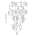
- the reference numeral 1 designates terminals for an address input
- the reference numeral 2 designates an edge detector which detects the change of the input address signal.
- the reference numeral 3 designates a NOR gate to which the outputs of the edge detectors 2 are input.
- the reference numeral 4 designates a pre-charge signal generator which generates a pre-charge signal ⁇ p.
- the reference numeral 5 designates a word line control circuit which controls the word line B so as to select a desired memory cell.
- the reference numeral 6 designates a memory cell
- the reference numeral 7 designates a Y-address decoder
- the reference numeral 8 designates a sense amplifier for amplifying the output signal from the memory cell 6.
- the reference numeral 9 designates an output buffer for taking out the output signal to the outside.
- the reference symbols A, B, C, and D designate a pre-charge signal (óp) line, a word line (WL), a pair of bit lines (BL), and an input/output (I/O) lines, respectively.
- the reference symbol E designates the two output lines of the sense amplifier 8.
- the reference symbol Q 1 designates a transistor for charging the bit lines C
- the reference symbol Q 2 designates a switching transistor for connecting or disconnecting between the bit lines C and the I/O lines D.
- the device will be operated as follows:
- the P-channel transistor Q1 turns on, and charges the bit lines C and the I/O lines D up to the "H” level. Then, the output lines E of the sense amplifier 8 are reset to "L” level. The pre-charge signal ⁇ p recovers to "H” level at the timing t 2 after the charging is completed.
- the word line control circuit 5 operates to make the word line B rise to the "H" level after the pre-charge signal ⁇ p becomes "H” level.
- the memory cell 6 is driven by this rising of the word line B, and either of a pair of bit lines C is discharged to become “L” level in accordance with the content of the memory cell 6.
- the I/O lines D change in the same way as either pair of the bit lines C to which the I/O lines D are connected through corresponding pair of transistors Q 2 which are turned on by the output of the corresponding Y-address decoder 7.
- the flowing current Icc through the device throughout this operation is only a charging current from the timing t 1 to t 3 , and no current flows after the timing t 3 when the operation is completed. Accordingly, the average current'in one cycle becomes small to a great extent. However, in this system, all the bit lines are charged at the same time, resulting in a sharp rising and falling in the current (Icc) waveform.
- the present invention is directed to solve the problems pointed above, and has for its object to provide an improved semiconductor memory device wherein the voltage amplitude of the bit lines is reduced, resulting in reduced charging currents.
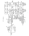
- a semiconductor memory device constituting a static Random Access Memory of internally synchronized circuitry system, which comprises: a detecting circuit intended to detect the completion of operation of a sense amplifier; and a control circuit intended to make the word line in an unselected state upon reception of the output signal from the detecting circuit.
- the reference numerals 2 1 to 2 s designate edge detectors each of which detects the change of each bit of the X-address input which is input thereto. Each edge detector outputs a one-shot pulse when each bit of the X-address input changes from "H" to "L” or from "L” to "H”.
- the reference numeral 3 designates a NOR gate to which all of the outputs of the edge detectors 2 1 to 2 are input. The NOR gate 3 outputs a pulse signal when any one of the edge detectors 2 1 to 2 outputs a one-shot pulse.
- the reference numeral 4 designates a pre-charge signal generator which outputs a negative one-shot pulse of a predetermined period when it receives the pulse signal from the NOR gate 3.
- the output of the pre-charge signal generator 4 is connected to the control electrodes of the pair of charging transistors Ql, Ql so as to turn ON the charging transistors while the negative one-shot pulse is generated.
- the reference numeral 5 designates a word line control circuit which outputs a signal of "H" of a predetermined period after the falling of the negative one-shot pulse from the pre-charge signal generator 4 upon reception of the pulse signal from the NOR gate 3.
- the edge detectors 21 to 2 S , the NOR gate 3, the pre-charge signal generator 4 and the word line control circuit 5 are constituted under the construction shown in Fig. 3 in Page 15 of DIGEST OF TECHNICAL PAPERS OF 1982 SYMPOSIUM ON VLSI TECHNOLOGY promoted by The Japan Society of Applied Physics and the IEEE Electron Devices Society.
- the reference numerals 6 11 to 6 mn designate m x n static memory cells arrayed in a matrix of m rows and n columns.
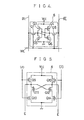
- Each memory cell is represented by a well-known CMOS static memory cell constituted by two P-channel MOS transistors Q3, Q4 and four N-channel MOS transistors Q5 to Q8 as shown in Figure 4.
- Each memory cell outputs complementary signals from corresponding pair of bit lines BL, BL. In the Figure, only four memory cells are typically illustrated.
- the reference numerals 7 1 to 7 n designate Y-decoders to which the Y-address input are input, and to the output whereof the control electrodes of the pair of switching transistors Q2, Q2 are connected.
- the Y-address decoders are intended to turn on the pair of switching transistors Q2, Q2 which are connected to the memory cells to be selected and to turn off the pair of switching transistors Q2, Q2 which are connected to the memory cells not to be selected.
- the numeral 8 designates a sense amplifier which, connected to the I/O and I/O lines, amplifies the signals of the I/O and I/O lines and outputs the amplified signal.
- the sense amplifier 8 is represented by the circuit shown in Figure 5, constituted by four P-channel MOS transistors Q9 to Q12 and two N-channel MOS transistors Q13, Q14.
- the numerals 10 1 to 10 m designate X-decoders to which the X-address input is input and to the output whereof the word lines WL 1 to WL are connected.
- the X-decoders are activated upon reception of the output signal of "H" level from the word line control circuit 5, and make the word lines connected to the memory cells to be selected by the X-address input "H" level, making the word lines connected to the memory cells not to be selected being held at "L” level.
- the reference numeral 11 designates a detecting circuit intended to detect the completion of operation of a sense amplifier 8 and output an output signal to the line F.
- the detecting circuit 11 is constituted by a NOR gate to which the output signals E, E of the sense amplifier 8 are input.
- the numerals 12 1 to 12 m designate AND gates to one input whereof the output of the X-decoders 10 1 to 10 m are connected, to other input whereof the output of the detecting circuit 11 is connected, and to the output whereof the word lines WL 1 to WL m are connected.
- the current flowing through a reading operation from one selected memory cell only includes a charging current which flows from the timing t 1 to t 3 , and no current flows after the timing t 3 to the pre-charging timing (corresponding to the t l ) in the next reading operation from the next selected memory cell. Furthermore, unnecessary discharges in the bit lines are prevented by separating the memory cell from the bit lines after reading data from the memory cell, that is, after the timing t 5 1
- the voltage amplitude of the bit lines becomes small which bit lines should be charged up at the next cycle, thereby reducing charging currents to a great extent. It is possible to attain a greatly reduced power consumption, and to smooth the rising and falling of the current waveform as well as to obtain a static operation with reduced noises.
- FIG. 7 Another embodiment of the present invention is illustrated in Figure 7. Different from the embodiment in Figure 3, there is provided an AND gate 12 between the word line control circuit 5 and the X-decoders 10 1 to 10 m , and each X-decoder 10 1 to 10 m is connected to each word line WL 1 to WL m .
- This embodiment has an advantage of reducing the number of AND gates as well as the same advantages as those of the embodiment in Figure 3.
- the memory cell is disconnected from the sense amplifier after the data are read out therefrom based upon the detection of the change of the output from the sense amplifier. This produces an effect of reducing the voltage amplitude of the bit lines, resulting in reduced charging currents.
Landscapes
- Engineering & Computer Science (AREA)
- Microelectronics & Electronic Packaging (AREA)
- Static Random-Access Memory (AREA)
- Dram (AREA)
Applications Claiming Priority (2)
| Application Number | Priority Date | Filing Date | Title |
|---|---|---|---|
| JP58170679A JPS6061985A (ja) | 1983-09-14 | 1983-09-14 | 半導体記憶装置 |
| JP170679/83 | 1983-09-14 |
Publications (3)
| Publication Number | Publication Date |
|---|---|
| EP0139385A2 true EP0139385A2 (de) | 1985-05-02 |
| EP0139385A3 EP0139385A3 (en) | 1986-10-22 |
| EP0139385B1 EP0139385B1 (de) | 1990-02-21 |
Family
ID=15909379
Family Applications (1)
| Application Number | Title | Priority Date | Filing Date |
|---|---|---|---|
| EP84305617A Expired EP0139385B1 (de) | 1983-09-14 | 1984-08-17 | Halbleiterspeicheranordnung |
Country Status (4)
| Country | Link |
|---|---|
| US (1) | US4625298A (de) |
| EP (1) | EP0139385B1 (de) |
| JP (1) | JPS6061985A (de) |
| DE (1) | DE3481395D1 (de) |
Cited By (4)
| Publication number | Priority date | Publication date | Assignee | Title |
|---|---|---|---|---|
| EP0251734A3 (en) * | 1986-06-30 | 1989-07-12 | Sony Corporation | Static random-access memory devices |
| EP0226616A4 (de) * | 1985-08-05 | 1990-01-08 | Motorola Inc | Asynchrone reihen- und spaltensteuerung. |
| EP0304591A3 (en) * | 1987-08-18 | 1990-08-16 | Siemens Aktiengesellschaft | Semiconductor memory with signal change detector circuit |
| GB2251325A (en) * | 1990-12-28 | 1992-07-01 | Samsung Electronics Co Ltd | Circuit for controlling the output of a sense amplifier |
Families Citing this family (10)
| Publication number | Priority date | Publication date | Assignee | Title |
|---|---|---|---|---|
| JPS6074194A (ja) * | 1983-09-29 | 1985-04-26 | Nec Corp | メモリ回路 |
| JPS61253695A (ja) * | 1985-05-07 | 1986-11-11 | Hitachi Ltd | 半導体記憶装置 |
| JPH0640439B2 (ja) * | 1986-02-17 | 1994-05-25 | 日本電気株式会社 | 半導体記憶装置 |
| JPS63211190A (ja) * | 1987-02-26 | 1988-09-02 | Nec Corp | メモリ回路用内部クロツク信号発生器 |
| JP2555372B2 (ja) * | 1987-09-09 | 1996-11-20 | 日本電気アイシーマイコンシステム 株式会社 | 半導体集積回路 |
| JPH01158694A (ja) * | 1987-12-15 | 1989-06-21 | Mitsubishi Electric Corp | 半導体ダイナミックram |
| KR0141494B1 (ko) * | 1988-01-28 | 1998-07-15 | 미다 가쓰시게 | 레벨시프트회로를 사용한 고속센스 방식의 반도체장치 |
| JPH01294294A (ja) * | 1988-05-20 | 1989-11-28 | Mitsubishi Electric Corp | 半導体記憶装置 |
| US5404327A (en) * | 1988-06-30 | 1995-04-04 | Texas Instruments Incorporated | Memory device with end of cycle precharge utilizing write signal and data transition detectors |
| DE10105285B4 (de) * | 2001-02-06 | 2008-01-10 | Infineon Technologies Ag | Halbleiterspeicher mit Precharge-Steuerung |
Family Cites Families (6)
| Publication number | Priority date | Publication date | Assignee | Title |
|---|---|---|---|---|
| US4103345A (en) * | 1975-04-28 | 1978-07-25 | Tokyo Shibaura Electric Co., Ltd. | Semiconductor memory with data detection circuit |
| US4024512A (en) * | 1975-06-16 | 1977-05-17 | Fairchild Camera And Instrument Corporation | Line-addressable random-access memory |
| US4150441A (en) * | 1978-03-20 | 1979-04-17 | Microtechnology Corporation | Clocked static memory |
| JPS54161876A (en) * | 1978-06-13 | 1979-12-21 | Nippon Telegr & Teleph Corp <Ntt> | Driving system for semiconductor integrated circuit |
| JPS59914B2 (ja) * | 1979-08-23 | 1984-01-09 | 富士通株式会社 | 半導体記憶装置 |
| GB2070372B (en) * | 1980-01-31 | 1983-09-28 | Tokyo Shibaura Electric Co | Semiconductor memory device |
-
1983
- 1983-09-14 JP JP58170679A patent/JPS6061985A/ja active Granted
-
1984
- 1984-08-16 US US06/641,551 patent/US4625298A/en not_active Expired - Lifetime
- 1984-08-17 EP EP84305617A patent/EP0139385B1/de not_active Expired
- 1984-08-17 DE DE8484305617T patent/DE3481395D1/de not_active Expired - Lifetime
Cited By (6)
| Publication number | Priority date | Publication date | Assignee | Title |
|---|---|---|---|---|
| EP0226616A4 (de) * | 1985-08-05 | 1990-01-08 | Motorola Inc | Asynchrone reihen- und spaltensteuerung. |
| EP0251734A3 (en) * | 1986-06-30 | 1989-07-12 | Sony Corporation | Static random-access memory devices |
| US5034924A (en) * | 1986-06-30 | 1991-07-23 | Sony Corporation | Static random access memory device with pull-down control circuit |
| EP0304591A3 (en) * | 1987-08-18 | 1990-08-16 | Siemens Aktiengesellschaft | Semiconductor memory with signal change detector circuit |
| GB2251325A (en) * | 1990-12-28 | 1992-07-01 | Samsung Electronics Co Ltd | Circuit for controlling the output of a sense amplifier |
| GB2251325B (en) * | 1990-12-28 | 1994-10-12 | Samsung Electronics Co Ltd | Circuit for controlling the output of a sense amplifier |
Also Published As
| Publication number | Publication date |
|---|---|
| US4625298A (en) | 1986-11-25 |
| DE3481395D1 (de) | 1990-03-29 |
| JPS6061985A (ja) | 1985-04-09 |
| EP0139385B1 (de) | 1990-02-21 |
| JPH0312397B2 (de) | 1991-02-20 |
| EP0139385A3 (en) | 1986-10-22 |
Similar Documents
| Publication | Publication Date | Title |
|---|---|---|
| EP0643393B1 (de) | Halbleiterspeicheranordnung mit Spannung-Erhöhungsschaltung | |
| US4389705A (en) | Semiconductor memory circuit with depletion data transfer transistor | |
| EP0199501B1 (de) | CMOS-Stromdetektorverstärker | |
| EP0196586B1 (de) | Statische Halbleiterspeicheranordnung | |
| US4933906A (en) | Non-volatile semiconductor memory device | |
| US5243573A (en) | Sense amplifier for nonvolatile semiconductor storage devices | |
| EP0211232B1 (de) | Halbleiterspeicher mit einem Leseverfahren in einem grossen Speisespannungsbereich | |
| US4625298A (en) | Semiconductor memory device | |
| EP0301588A2 (de) | Halbleiterspeicheranordnung | |
| US6711088B2 (en) | Semiconductor memory device | |
| US4417329A (en) | Active pull-up circuit | |
| US5402378A (en) | Circuit for generating a clock signal to separate bit lines in a semiconductor memory device | |
| US5323345A (en) | Semiconductor memory device having read/write circuitry | |
| US4912677A (en) | Programmable logic device | |
| US6600672B2 (en) | Semiconductor memory device | |
| US5245578A (en) | DRAM with a two stage voltage pull-down sense amplifier | |
| US4689771A (en) | Memory with improved write mode to read mode transition | |
| US4451907A (en) | Pull-up circuit for a memory | |
| US5278788A (en) | Semiconductor memory device having improved controlling function for data buses | |
| EP0061271B1 (de) | Dynamische MOS-Speicheranordnung | |
| EP0238366B1 (de) | Datenleseschaltung zum Gebrauch in Halbleiterspeichereinrichtungen | |
| EP0158028A2 (de) | Direktzugriffspeicheranordnung | |
| KR930009463B1 (ko) | 반도체 메모리장치와 감지 증폭기 | |
| US4661926A (en) | Bit line gain circuit for read only memory | |
| US4628250A (en) | Power conserving CMOS reference voltage source |
Legal Events
| Date | Code | Title | Description |
|---|---|---|---|
| PUAI | Public reference made under article 153(3) epc to a published international application that has entered the european phase |
Free format text: ORIGINAL CODE: 0009012 |
|
| AK | Designated contracting states |
Designated state(s): DE FR GB |
|
| PUAL | Search report despatched |
Free format text: ORIGINAL CODE: 0009013 |
|
| AK | Designated contracting states |
Kind code of ref document: A3 Designated state(s): DE FR GB |
|
| 17P | Request for examination filed |
Effective date: 19870312 |
|
| 17Q | First examination report despatched |
Effective date: 19880324 |
|
| GRAA | (expected) grant |
Free format text: ORIGINAL CODE: 0009210 |
|
| AK | Designated contracting states |
Kind code of ref document: B1 Designated state(s): DE FR GB |
|
| REF | Corresponds to: |
Ref document number: 3481395 Country of ref document: DE Date of ref document: 19900329 |
|
| ET | Fr: translation filed | ||
| PLBE | No opposition filed within time limit |
Free format text: ORIGINAL CODE: 0009261 |
|
| STAA | Information on the status of an ep patent application or granted ep patent |
Free format text: STATUS: NO OPPOSITION FILED WITHIN TIME LIMIT |
|
| 26N | No opposition filed | ||
| REG | Reference to a national code |
Ref country code: GB Ref legal event code: 746 Effective date: 19950809 |
|
| REG | Reference to a national code |
Ref country code: FR Ref legal event code: D6 |
|
| PGFP | Annual fee paid to national office [announced via postgrant information from national office to epo] |
Ref country code: GB Payment date: 19980810 Year of fee payment: 15 |
|
| PGFP | Annual fee paid to national office [announced via postgrant information from national office to epo] |
Ref country code: FR Payment date: 19980814 Year of fee payment: 15 |
|
| PGFP | Annual fee paid to national office [announced via postgrant information from national office to epo] |
Ref country code: DE Payment date: 19980821 Year of fee payment: 15 |
|
| PG25 | Lapsed in a contracting state [announced via postgrant information from national office to epo] |
Ref country code: GB Free format text: LAPSE BECAUSE OF NON-PAYMENT OF DUE FEES Effective date: 19990817 |
|
| GBPC | Gb: european patent ceased through non-payment of renewal fee |
Effective date: 19990817 |
|
| PG25 | Lapsed in a contracting state [announced via postgrant information from national office to epo] |
Ref country code: FR Free format text: LAPSE BECAUSE OF NON-PAYMENT OF DUE FEES Effective date: 20000428 |
|
| PG25 | Lapsed in a contracting state [announced via postgrant information from national office to epo] |
Ref country code: DE Free format text: LAPSE BECAUSE OF NON-PAYMENT OF DUE FEES Effective date: 20000601 |
|
| REG | Reference to a national code |
Ref country code: FR Ref legal event code: ST |