EP0158028A2 - Direktzugriffspeicheranordnung - Google Patents
Direktzugriffspeicheranordnung Download PDFInfo
- Publication number
- EP0158028A2 EP0158028A2 EP85101311A EP85101311A EP0158028A2 EP 0158028 A2 EP0158028 A2 EP 0158028A2 EP 85101311 A EP85101311 A EP 85101311A EP 85101311 A EP85101311 A EP 85101311A EP 0158028 A2 EP0158028 A2 EP 0158028A2
- Authority
- EP
- European Patent Office
- Prior art keywords
- signal
- write
- signal generator
- bit lines
- control means
- Prior art date
- Legal status (The legal status is an assumption and is not a legal conclusion. Google has not performed a legal analysis and makes no representation as to the accuracy of the status listed.)
- Withdrawn
Links
- 230000004044 response Effects 0.000 claims abstract description 25
- 230000007704 transition Effects 0.000 claims description 9
- 230000000295 complement effect Effects 0.000 abstract description 4
- 239000000872 buffer Substances 0.000 description 5
- 239000004065 semiconductor Substances 0.000 description 4
- 238000001514 detection method Methods 0.000 description 3
- 239000011159 matrix material Substances 0.000 description 3
- 230000007257 malfunction Effects 0.000 description 2
- 238000010586 diagram Methods 0.000 description 1
- 230000010354 integration Effects 0.000 description 1
- 230000003068 static effect Effects 0.000 description 1
Images

Classifications
-
- G—PHYSICS
- G11—INFORMATION STORAGE
- G11C—STATIC STORES
- G11C11/00—Digital stores characterised by the use of particular electric or magnetic storage elements; Storage elements therefor
- G11C11/21—Digital stores characterised by the use of particular electric or magnetic storage elements; Storage elements therefor using electric elements
-
- G—PHYSICS
- G11—INFORMATION STORAGE
- G11C—STATIC STORES
- G11C7/00—Arrangements for writing information into, or reading information out from, a digital store
- G11C7/12—Bit line control circuits, e.g. drivers, boosters, pull-up circuits, pull-down circuits, precharging circuits, equalising circuits, for bit lines
-
- G—PHYSICS
- G11—INFORMATION STORAGE
- G11C—STATIC STORES
- G11C11/00—Digital stores characterised by the use of particular electric or magnetic storage elements; Storage elements therefor
- G11C11/21—Digital stores characterised by the use of particular electric or magnetic storage elements; Storage elements therefor using electric elements
- G11C11/34—Digital stores characterised by the use of particular electric or magnetic storage elements; Storage elements therefor using electric elements using semiconductor devices
- G11C11/40—Digital stores characterised by the use of particular electric or magnetic storage elements; Storage elements therefor using electric elements using semiconductor devices using transistors
Definitions
- the present invention generally relates to a semiconductor memory device and, more particularly, to a random access memory (RAM) device having bit lines which are precharged whenever data is read and written.
- RAM random access memory
- a static RAM using a transition detector in order to precharge the bit line as fast as possible after the address signal was updated.
- this RAM a plurality of memory cells are arranged like a matrix on the semiconductor chip.
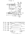
- Fig. 1 shows memory cells Ml to ML of the same column in this matrix together with a data writing circuit.
- This RAM has a bit line Bl connected to data terminals of the memory cells Ml to ML and a bit line B2 connected to complement data terminals of the memory cells Ml to ML.
- the bit line Bl is connected through an n-channel MOS transistor Ql to a power source terminal VDD, and at the same time, it is also grounded through n-channel MOS transistors Q2 and Q3 in this order.
- the bit line B2 is connected through an n-channel MOS transistor Q4 to the power source terminal VDD and is also grounded through n-channel MOS transistors Q5 and Q3 in this order.
- the conductions of the MOS transistors Ql and Q4 are controlled by a precharge controller 10.
- the precharge controller 10 has a transition detector for detecting the updating of an address signal and a signal generator for supplying drive signal to the MOS transistors Ql and Q4 for a predetermined period in response to an output signal of this transition detector.
- the bit lines Bl and B2 are precharged during the time period in which the MOS transistors Ql and Q4 are kept conductive due to the drive signal.
- the voltage difference between the bit lines Bl and B2 is detected by a sense amplifier 12 for reading data.
- this RAM has a decoding circuit 14 to decode an address signal A.
- the decoding circuit 14 includes a row decoder and a column decoder.
- One of the memory cells Ml to ML and the MOS transistor Q3 receive drive signals which are simultaneously generated from the row and column decoders in accordance with a particular address signal.
- a write instruction WI is supplied to a writing controller 16.
- the writing controller 16 supplies a write permitting signal WS, which is maintained at a high level for a predetermined period, to a data setting circuit 18 in response to the write instruction WI.
- the data setting circuit 18 is provided to control the conductions of the MOS transistors Q2 and Q5 and includes NAND gates 20 and 22 and inverters 24 and 26.
- the data setting circuit 18 maintains the MOS transistors Q2 and Q5 in a non-conductive state during the period in which no write permitting signal is supplied from the writing controller 16.
- the data setting circuit 18 operates so as to selectively make one of the MOS transistors Q2 and Q5 conductive and to make the other non-conductive in accordance with data DI for writing.
- the write instruction WI, address signal A and writing data DI are supplied to the RAM from the outside.
- the write instruction WI is ordinarily set so as to rise simultaneously with the updating of the address signal A or after this updating. For instance, it is assumed that the address signal A is updated at time T ⁇ as shown in Fig. 2A, and the write instruction WI is simultaneously supplied as shown in Fig. 2D. Then, in response to the updating of the address signal A, the precharge controller 10 immediately supplies a drive signal as shown in Fig.
- a drive signal as shown in Fig. 2C is supplied to the memory cell Ml from the row decoder of the decoding circuit 14 at time T2 while the bit lines Bl and B2 are respectively precharged through the MOS transistors Ql and Q4.
- the MOS transistor Q3 is made conductive due to the column decoder of the decoding circuit 14.
- the writing controller 16 In response to the write instruction WI, the writing controller 16 generates the write permitting signal WS at a high level at time T3 as shown in Fig. 2E and supplies this signal WS to the data setting circuit 18.
- the data setting circuit 18 holds both MOS transistors Q2 and Q5 non-conductive during the time in which the signal WS is not supplied. When this signal WS is supplied, the data setting circuit 18 selectively renders either one of the MOS transistors Q2 and Q5 conductive in accordance with the data DI. Due to this, in association with the completion of a precharge period TP of the bit lines Bl and B2 at time T4, either one of the bit lines Bl and B2 is set at a predetermined voltage, and the other is set at a ground voltage.
- the memory cell Ml stores the voltages of the bit lines Bl and B2 as the data.
- the data DI is determined after time T0, and this determined value is maintained by the time period in which the data is correctly written.
- a data writing period TW is the time required for the memory cell Ml to store the data.
- the address signal A is again updated at time T5 and the write instruction WI simultaneously trails as shown in Fig. 2D.
- the writing controller 16 stops the generation of the write permitting signal WS at time T6. This stop timing is set before the time when the decoding circuit 14 interrupts the drive signal shown in Fig. 2C being sent to the memory cell Ml in response to the address signal A which has been updated at time T5.
- the write permitting signal WS has to be generated while the particular memory cell, for example, the memory cell Ml, is driven and has to disappear before another memory cell which is driven next is selected. Therefore, the response time of the writing controller 16 and the time period for the generation of the write permitting signal WS are ordinarily set using a delay circuit such that the leading time is slow and the trailing time is fast.
- the data writing period TW overlaps for the precharge period TP.
- this overlap period (from time T3 to time T4), a great amount of direct current flows from the power source terminal VDD to the ground through either one of the path formed of the MOS transistor Ql, bit line Bl, and MOS transistors Q2 and Q3 and the path formed of the MOS transistor Q4, bit line B2, and MOS transistors Q5 and Q3.
- this direct current flows, the potential of the power source terminal VDD drops to a value lower than the predetermined value, so that the noises will have occurred on the power source line and other bit lines Bl-2 to Bl-N and B2-2 to B2-N.
- the bit line of the path through which no direct current flows may be at a voltage lower than a predetermined precharge voltage. This causes the RAM to store erroneous data in the memory cell.
- the sense amplifier 12 belongs to the type of latching the bit line voltage, there is a high possibility such that readout data DO will have been changed to an erroneous value due to the foregoing voltage decrease of the bit line.
- a random access memory device comprising: a bit line; a plurality of memory cells connected to this bit line; a decoding circuit to designate in accordance with an address signal the memory cell in which data should be stored; a precharge control circuit to precharge the bit line in response to the updating of the address signal for a predetermined time period and to generate an end signal indicative of the completion of this predetermined period; a data setting circuit to set the voltage in accordance with the data to the bit line in response to a write permitting signal; and a write control circuit to supply the write permitting signal to the data setting circuit in response to a write instruction and to the end signal.
- the write permitting signal is generated by the write control circuit in response to the end signal and to the write instruction. Due to this, the bit line is precharged, and thereafter this bit line is, for example, discharged in accordance with the data. Namely, the bit line is not discharged, while it is precharged, so that the malfunction of this RAM due to the voltage decrease of the bit line is prevented.
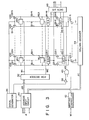
- the RAM of Fig. 3 has, for example, (L x N) memory cells Mll to MIN; ...; ML1 to MLN which are formed like a matrix on a semiconductor chip.
- Word lines Wl to WL are formed along the rows of the memory cells Mll to MLN.
- First bit lines Bl-I to Bl-N and second bit lines B2-1 to B2-N are formed along the columns of the memory cells.
- the memory cells of the same row, for instance, the memory cells Mll to M1N are selected through the word line Wl.
- the data terminals of the memory cells of the same column e.g., of the memory cells M11 to ML1 are connected to the bit line Bl-1, while the complement data terminals of the memory cells Mll to ML1 are connected to the bit line B2-1.
- the data terminals and complement data terminals of the memory cells of each of the other columns are also connected to the corresponding bit lines in a similar manner as above.
- This RAM further has n-channel MOS transistors Q1-1 to Ql-N, Q2-1 to Q2-N, Q3-1 to Q3-N, Q4-1 to Q4-N, and Q5-1 to Q5-N in correspondence to the columns of the memory cells Mll to MLN.
- bit line Bl-l is connected through the current path of the MOS transistor Ql-l to the power source terminal VDD, and at the same time, it is grounded through the current paths of the MOS transistors Q3-1 and Q5-1 in this order.
- the bit line B2-1 is connected through the current path of the MOS transistor Q2-1 to the power source terminal VDD and is grounded through the MOS transistors Q4-1 and Q5-1 in this order.
- the other transistors are also connected to the corresponding bit lines in a similar manner as above.
- the memory cells of the same column e.g., the memory cells Mll to ML1 are selected due to the conduction of the MOS transistor Q5-1.
- An address input circuit 30 includes buffers to receive the address signal A and a transition detector to detect the updating of the address signal A.
- the address signal A is divided into a row address signal AR and a column address signal AC by the address input circuit 30, and these signals are supplied to a row decoder 32 and a column decoder 34, respectively.
- the row decoder 32 selectively supplies a drive signal to one of the word lines Wl to WL in accordance with the row address signal AR.
- the column decoder 34 selectively supplies a drive signal to a predetermined number of memory cells among the MOS transistors Q5-1 to Q5-N in accordance with the column address signal AC.
- the conductions of the MOS transistors Ql-1 to Ql-N and Q2-1 to Q2-N are controlled by an output signal from a first output terminal of a signal generator 36.
- the signal generator 36 generates high-level signals from first and second output terminals for a predetermined time period in response to a detection signal supplied from the transition detector in the address input circuit 30. After the elapse of this predetermined period, the signal generator 36 generates low-level signals from the first and second output terminals.
- the bit lines Bl-1 to Bl-N and B2-1 to B2-N are precharged during the period in which the MOS transistors Ql-I to Ql-N and Q2-1 to Q2-N are kept conductive due to the high-level signal supplied from the first terminal of the signal generator 36.
- the second output terminal of the signal generator 36 is connected to a first input terminal of an AND gate 40 through an inverter 38.
- the write instruction WI is supplied to a writing controller 42.
- the writing controller 42 supplies a high-level signal to a second input terminal of the AND gate 40 for a predetermined time period in response to the write instruction WI.
- the AND gate 40 generates the write permitting signal WS in response to the input signals at high level.
- This RAM has sense amplifiers 44-1 to 44-N and data setting circuits 46-1 to 46-N in correspondence to the columns of the memory cells and also has a data input/output circuit 48.
- the data input/output circuit 48 includes input buffers and output buffers, and the write data is supplied through these input buffers to the corresponding data setting circuits.
- the data setting operations of the data setting circuits 46-1 to 46-N are controlled by the AND gate 40.
- Each data setting circuit e.g., the data setting circuit 46-1, holds the MOS transistors Q3-1 and Q4-1 non-conductive irrespective of the write data during the period in which a low-level signal is supplied from the AND gate 40.
- the data setting circuit 46-1 When a high-level signal is supplied as the write permitting signal WS, the data setting circuit 46-1 renders either one of the MOS transistors Q3-1 and Q4-1 conductive in accordance with the write data. For instance, when the data is "1", the low-level signal and high-level signal are respectively supplied to the gates of the MOS transistors Q3-1 and Q4-1. On the contrary, when the data is "0”, the high-level signal and low-level signal are respectively supplied to the gates of the MOS transistors Q3-1 and Q4-1.
- the other MOS transistors Q3-2 to Q3-N and Q4-2 to Q4-N are also controlled by the corresponding data setting circuits 46-2 to 46-N in a similar manner as above.
- the sense amplifiers 44-1 to 44-N respectively supply output signals corresponding to the voltage differences between the first and second bit lines Bl-1 and B2-l; ..., Bl-N and B2-N as readout data to output buffers in the data input/output circuit 48.
- the transition detector in the address input circuit 30 supplies a detection signal to the signal generator 36.
- the signal generator 36 supplies a high-level signal as shown in Fig. 4C to the MOS transistors Ql-1 to Ql-N and Q2-1 to Q2-N for the period from time Tl to time T3.
- the bit lines Bl-1 to Bl-N and B2-1 to B2-N are precharged.
- the row decoder 32 supplies a drive signal to the memory cells of the row corresponding to the row address signal AR, while the column decoder 34 makes predetermined MOS transistors among the MOS transistors Q5-1 to Q5-N conductive in accordance with the column address signal AC.
- the writing controller 42 generates a high-level signal after time T2 as shown in Fig. 4D.
- the AND gate 40 supplies a high-level signal, as shown in Fig. 4E, as a write permitting signal WS to the data setting circuits 46-1 to. 46-N in response to this trailing edge.
- either one of the MOS transistors Q3-1 and Q4-1 is made conductive due to the data setting circuit 46-1.
- the MOS transistor Q5-1 is kept conductive due to the column decoder 34, one of the bit lines Bl and B2 precharged until time T3 is discharged.
- the memory cell selected by the row decoder 32 stores the voltages of the bit lines Bl and B2 as the data.
- the signal generator 36 again generates a high-level signal to precharge after time T6, as shown in Fig. 4C.
- the output signal of the writing controller 42 also trails at time T5, as shown in Fig. 4D.
- the AND gate 40 In response to the leading edge of the output signal of the signal generator 36 or to the trailing edge of the output signal of the writing controller 42, the AND gate 40 generates a low-level signal at time T7, as shown in Fig. 4E. Namely, the write permitting signal WS is interrupted.
- the AND gate 40 generates the write permitting signal WS with respect to the output signal of the signal generator 36 and to the output signal of the writing controller 42. That is, the precharge period TP of the bit lines and the writing period TW of the data are assigned to the different time bands. Therefore, a large current does not flow from the power source terminal VDD to the ground through the bit lines B1-1 to Bl-N and B2-1 to B2-N. Thus, the malfunction due to the voltage decrease of the power source terminal VDD does not occur in this RAM, and the noise on the power source line is also sufficiently reduced.
Landscapes
- Engineering & Computer Science (AREA)
- Computer Hardware Design (AREA)
- Microelectronics & Electronic Packaging (AREA)
- Static Random-Access Memory (AREA)
Applications Claiming Priority (2)
| Application Number | Priority Date | Filing Date | Title |
|---|---|---|---|
| JP35494/84 | 1984-02-27 | ||
| JP59035494A JPS60179993A (ja) | 1984-02-27 | 1984-02-27 | ランダムアクセスメモリ |
Publications (2)
| Publication Number | Publication Date |
|---|---|
| EP0158028A2 true EP0158028A2 (de) | 1985-10-16 |
| EP0158028A3 EP0158028A3 (de) | 1987-10-07 |
Family
ID=12443297
Family Applications (1)
| Application Number | Title | Priority Date | Filing Date |
|---|---|---|---|
| EP85101311A Withdrawn EP0158028A3 (de) | 1984-02-27 | 1985-02-07 | Direktzugriffspeicheranordnung |
Country Status (3)
| Country | Link |
|---|---|
| EP (1) | EP0158028A3 (de) |
| JP (1) | JPS60179993A (de) |
| KR (1) | KR850006119A (de) |
Cited By (3)
| Publication number | Priority date | Publication date | Assignee | Title |
|---|---|---|---|---|
| EP0405055A3 (de) * | 1989-06-23 | 1994-03-30 | Ibm | |
| GB2338808A (en) * | 1998-06-23 | 1999-12-29 | Mitel Semiconductor Ltd | Semiconductor memory |
| CN109416919A (zh) * | 2016-07-08 | 2019-03-01 | 高通股份有限公司 | 重叠的预充电和数据写入 |
Families Citing this family (4)
| Publication number | Priority date | Publication date | Assignee | Title |
|---|---|---|---|---|
| JP2561086B2 (ja) * | 1987-04-09 | 1996-12-04 | 三菱電機株式会社 | メモリ装置 |
| JPH07118196B2 (ja) * | 1988-12-28 | 1995-12-18 | 株式会社東芝 | スタティック型半導体メモリ |
| JPH0319196A (ja) * | 1989-06-16 | 1991-01-28 | Mitsubishi Electric Corp | ガリウム砒素半導体集積回路 |
| IT1252017B (it) * | 1991-11-28 | 1995-05-27 | Sgs Thomson Microelectronics | Struttura circuitale a registri distribuiti con lettura e scrittura autotemporizzate |
Family Cites Families (3)
| Publication number | Priority date | Publication date | Assignee | Title |
|---|---|---|---|---|
| JPS6057156B2 (ja) * | 1978-05-24 | 1985-12-13 | 株式会社日立製作所 | 半導体メモリ装置 |
| JPS5668990A (en) * | 1979-11-08 | 1981-06-09 | Nec Corp | Memory circuit |
| US4337525A (en) * | 1979-04-17 | 1982-06-29 | Nippon Electric Co., Ltd. | Asynchronous circuit responsive to changes in logic level |
-
1984
- 1984-02-27 JP JP59035494A patent/JPS60179993A/ja active Pending
-
1985
- 1985-01-31 KR KR1019850000612A patent/KR850006119A/ko not_active Abandoned
- 1985-02-07 EP EP85101311A patent/EP0158028A3/de not_active Withdrawn
Cited By (5)
| Publication number | Priority date | Publication date | Assignee | Title |
|---|---|---|---|---|
| EP0405055A3 (de) * | 1989-06-23 | 1994-03-30 | Ibm | |
| GB2338808A (en) * | 1998-06-23 | 1999-12-29 | Mitel Semiconductor Ltd | Semiconductor memory |
| GB2338808B (en) * | 1998-06-23 | 2002-02-27 | Mitel Semiconductor Ltd | Semiconductor memories |
| CN109416919A (zh) * | 2016-07-08 | 2019-03-01 | 高通股份有限公司 | 重叠的预充电和数据写入 |
| CN109416919B (zh) * | 2016-07-08 | 2020-02-28 | 高通股份有限公司 | 重叠的预充电和数据写入 |
Also Published As
| Publication number | Publication date |
|---|---|
| KR850006119A (ko) | 1985-09-28 |
| EP0158028A3 (de) | 1987-10-07 |
| JPS60179993A (ja) | 1985-09-13 |
Similar Documents
| Publication | Publication Date | Title |
|---|---|---|
| KR100211482B1 (ko) | 감소 칩 영역을 가진 반도체 메모리 소자 | |
| US4744063A (en) | Static memory utilizing transition detectors to reduce power consumption | |
| US6646938B2 (en) | Static memory having self-timing circuit | |
| US5608667A (en) | Ferroelectric memory automatically generating biasing pulse for plate electrode | |
| EP0136811B1 (de) | Bitleitungslast und Spalteschaltungen für einen Halbleiterspeicher | |
| EP0293339B1 (de) | Nichtflüchtige Speichereinrichtung, die eine grosse Zahl von Programmierungszyklen verträgt | |
| EP0128499B1 (de) | MOS-Speicher | |
| KR100328161B1 (ko) | 집적 회로 메모리 | |
| US4751683A (en) | Static semiconductor memory device comprising word lines each operating at three different voltage levels | |
| KR100310358B1 (ko) | 제로(0)전력으로고속프로그램가능한회로장치구조 | |
| EP0145488A2 (de) | Halbleiterspeicheranordnung | |
| US6580653B2 (en) | Current saving semiconductor memory and method | |
| EP0139385A2 (de) | Halbleiterspeicheranordnung | |
| KR0159454B1 (ko) | 반도체 메모리장치 | |
| US5572467A (en) | Address comparison in an inteagrated circuit memory having shared read global data lines | |
| EP0158028A2 (de) | Direktzugriffspeicheranordnung | |
| KR930001652B1 (ko) | 반도체 기억장치 | |
| US5265061A (en) | Apparatus for preventing glitch for semiconductor non-volatile memory device | |
| US5295098A (en) | Semiconductor memory device having high-speed three-state data output buffer circuit without voltage fluctuation on power voltage lines | |
| US5604704A (en) | Compound semiconductor static random access memory device equipped with precharging circuit controlled by boosted signal | |
| KR100299901B1 (ko) | 반도체 메모리장치 | |
| US6078531A (en) | Word line voltage supply circuit | |
| US4661926A (en) | Bit line gain circuit for read only memory | |
| US4628250A (en) | Power conserving CMOS reference voltage source | |
| US6487138B2 (en) | Semiconductor memory |
Legal Events
| Date | Code | Title | Description |
|---|---|---|---|
| PUAI | Public reference made under article 153(3) epc to a published international application that has entered the european phase |
Free format text: ORIGINAL CODE: 0009012 |
|
| 17P | Request for examination filed |
Effective date: 19850304 |
|
| AK | Designated contracting states |
Designated state(s): DE FR GB |
|
| PUAL | Search report despatched |
Free format text: ORIGINAL CODE: 0009013 |
|
| AK | Designated contracting states |
Kind code of ref document: A3 Designated state(s): DE FR GB |
|
| 17Q | First examination report despatched |
Effective date: 19880129 |
|
| STAA | Information on the status of an ep patent application or granted ep patent |
Free format text: STATUS: THE APPLICATION IS DEEMED TO BE WITHDRAWN |
|
| 18D | Application deemed to be withdrawn |
Effective date: 19891017 |
|
| RIN1 | Information on inventor provided before grant (corrected) |
Inventor name: ISOBE, MITSUOC/O PATENT DIVISION |