EP0140418B1 - Aktive Doppelweg-Gleichrichterschaltung - Google Patents
Aktive Doppelweg-Gleichrichterschaltung Download PDFInfo
- Publication number
- EP0140418B1 EP0140418B1 EP84201361A EP84201361A EP0140418B1 EP 0140418 B1 EP0140418 B1 EP 0140418B1 EP 84201361 A EP84201361 A EP 84201361A EP 84201361 A EP84201361 A EP 84201361A EP 0140418 B1 EP0140418 B1 EP 0140418B1
- Authority
- EP
- European Patent Office
- Prior art keywords
- output
- current
- transistors
- resistor
- collectors
- Prior art date
- Legal status (The legal status is an assumption and is not a legal conclusion. Google has not performed a legal analysis and makes no representation as to the accuracy of the status listed.)
- Expired
Links
Images



Classifications
-
- G—PHYSICS
- G01—MEASURING; TESTING
- G01R—MEASURING ELECTRIC VARIABLES; MEASURING MAGNETIC VARIABLES
- G01R19/00—Arrangements for measuring currents or voltages or for indicating presence or sign thereof
- G01R19/22—Arrangements for measuring currents or voltages or for indicating presence or sign thereof using conversion of AC into DC
-
- H—ELECTRICITY
- H02—GENERATION; CONVERSION OR DISTRIBUTION OF ELECTRIC POWER
- H02H—EMERGENCY PROTECTIVE CIRCUIT ARRANGEMENTS
- H02H3/00—Emergency protective circuit arrangements for automatic disconnection directly responsive to an undesired change from normal electric working condition with or without subsequent reconnection ; integrated protection
- H02H3/26—Emergency protective circuit arrangements for automatic disconnection directly responsive to an undesired change from normal electric working condition with or without subsequent reconnection ; integrated protection responsive to difference between voltages or between currents; responsive to phase angle between voltages or between currents
- H02H3/32—Emergency protective circuit arrangements for automatic disconnection directly responsive to an undesired change from normal electric working condition with or without subsequent reconnection ; integrated protection responsive to difference between voltages or between currents; responsive to phase angle between voltages or between currents involving comparison of the voltage or current values at corresponding points in different conductors of a single system, e.g. of currents in go and return conductors
- H02H3/33—Emergency protective circuit arrangements for automatic disconnection directly responsive to an undesired change from normal electric working condition with or without subsequent reconnection ; integrated protection responsive to difference between voltages or between currents; responsive to phase angle between voltages or between currents involving comparison of the voltage or current values at corresponding points in different conductors of a single system, e.g. of currents in go and return conductors using summation current transformers
-
- H—ELECTRICITY
- H02—GENERATION; CONVERSION OR DISTRIBUTION OF ELECTRIC POWER
- H02M—APPARATUS FOR CONVERSION BETWEEN AC AND AC, BETWEEN AC AND DC, OR BETWEEN DC AND DC, AND FOR USE WITH MAINS OR SIMILAR POWER SUPPLY SYSTEMS; CONVERSION OF DC OR AC INPUT POWER INTO SURGE OUTPUT POWER; CONTROL OR REGULATION THEREOF
- H02M7/00—Conversion of AC power input into DC power output; Conversion of DC power input into AC power output
- H02M7/02—Conversion of AC power input into DC power output without possibility of reversal
- H02M7/04—Conversion of AC power input into DC power output without possibility of reversal by static converters
- H02M7/12—Conversion of AC power input into DC power output without possibility of reversal by static converters using discharge tubes with control electrode or semiconductor devices with control electrode
- H02M7/21—Conversion of AC power input into DC power output without possibility of reversal by static converters using discharge tubes with control electrode or semiconductor devices with control electrode using devices of a triode or transistor type requiring continuous application of a control signal
- H02M7/217—Conversion of AC power input into DC power output without possibility of reversal by static converters using discharge tubes with control electrode or semiconductor devices with control electrode using devices of a triode or transistor type requiring continuous application of a control signal using semiconductor devices only
-
- G—PHYSICS
- G01—MEASURING; TESTING
- G01R—MEASURING ELECTRIC VARIABLES; MEASURING MAGNETIC VARIABLES
- G01R19/00—Arrangements for measuring currents or voltages or for indicating presence or sign thereof
- G01R19/0084—Measuring voltage only
-
- H—ELECTRICITY
- H02—GENERATION; CONVERSION OR DISTRIBUTION OF ELECTRIC POWER
- H02H—EMERGENCY PROTECTIVE CIRCUIT ARRANGEMENTS
- H02H1/00—Details of emergency protective circuit arrangements
- H02H1/0092—Details of emergency protective circuit arrangements concerning the data processing means, e.g. expert systems, neural networks
-
- H—ELECTRICITY
- H02—GENERATION; CONVERSION OR DISTRIBUTION OF ELECTRIC POWER
- H02M—APPARATUS FOR CONVERSION BETWEEN AC AND AC, BETWEEN AC AND DC, OR BETWEEN DC AND DC, AND FOR USE WITH MAINS OR SIMILAR POWER SUPPLY SYSTEMS; CONVERSION OF DC OR AC INPUT POWER INTO SURGE OUTPUT POWER; CONTROL OR REGULATION THEREOF
- H02M7/00—Conversion of AC power input into DC power output; Conversion of DC power input into AC power output
- H02M7/02—Conversion of AC power input into DC power output without possibility of reversal
- H02M7/04—Conversion of AC power input into DC power output without possibility of reversal by static converters
- H02M7/12—Conversion of AC power input into DC power output without possibility of reversal by static converters using discharge tubes with control electrode or semiconductor devices with control electrode
- H02M7/21—Conversion of AC power input into DC power output without possibility of reversal by static converters using discharge tubes with control electrode or semiconductor devices with control electrode using devices of a triode or transistor type requiring continuous application of a control signal
- H02M7/217—Conversion of AC power input into DC power output without possibility of reversal by static converters using discharge tubes with control electrode or semiconductor devices with control electrode using devices of a triode or transistor type requiring continuous application of a control signal using semiconductor devices only
- H02M7/219—Conversion of AC power input into DC power output without possibility of reversal by static converters using discharge tubes with control electrode or semiconductor devices with control electrode using devices of a triode or transistor type requiring continuous application of a control signal using semiconductor devices only in a bridge configuration
- H02M7/2195—Conversion of AC power input into DC power output without possibility of reversal by static converters using discharge tubes with control electrode or semiconductor devices with control electrode using devices of a triode or transistor type requiring continuous application of a control signal using semiconductor devices only in a bridge configuration the switches being synchronously commutated at the same frequency of the AC input voltage
-
- Y—GENERAL TAGGING OF NEW TECHNOLOGICAL DEVELOPMENTS; GENERAL TAGGING OF CROSS-SECTIONAL TECHNOLOGIES SPANNING OVER SEVERAL SECTIONS OF THE IPC; TECHNICAL SUBJECTS COVERED BY FORMER USPC CROSS-REFERENCE ART COLLECTIONS [XRACs] AND DIGESTS
- Y02—TECHNOLOGIES OR APPLICATIONS FOR MITIGATION OR ADAPTATION AGAINST CLIMATE CHANGE
- Y02B—CLIMATE CHANGE MITIGATION TECHNOLOGIES RELATED TO BUILDINGS, e.g. HOUSING, HOUSE APPLIANCES OR RELATED END-USER APPLICATIONS
- Y02B70/00—Technologies for an efficient end-user side electric power management and consumption
- Y02B70/10—Technologies improving the efficiency by using switched-mode power supplies [SMPS], i.e. efficient power electronics conversion e.g. power factor correction or reduction of losses in power supplies or efficient standby modes
Definitions
- the invention relates to an active double-sided rectifier circuit which is particularly suitable for a current transformer which is used, for example, in an earth leakage detector. This must be able to indicate very weak currents and, because they are installed in distributing boxes, must not have large dimensions. However, the invention is obviously not restricted to this use.
- the most usual circuit for rectifying a current from a current transformer is formed by a diode bridge composed of four diodes and connected to the secondary winding of the current transformer.
- This rectifier circuit has the advantage of double-sided rectification and consists of few, passive components, while the output is potential free, so that there is free choice in respect of direct current level.
- This known circuit nevertheless has disadvantages making it less suitable, for example, for earth leakage detectors.
- this loading will adversely affect the transmission of the current transformer.
- This transmission is ideal only with shot-circuited output terminals.
- the voltage drop across the diodes in the forward direction also influences the transmission. This voltage drop may be of the order of 600 mV in the case of an Si diode.
- FIGS 1 and 2 show equivalent circuit diagrams of current transformers.
- L is the self-induction of the secondary windings and R the output resistance.
- a small toroidal core transformer having 1000 turns has a self-inductance of about 5 H.
- the output voltage U o is:
- Figure 3 shows an example of a possible circuit with active components and single-sided rectification.
- the current transformer with a transmission ratio of 1:n is provided with a primary winding 1 and a secondary winding 2.
- a connection terminal of the secondary winding is connected via a capacitor 3 or a resistor 9, shown above it, to an input terminal of the operational amplifier 4, while the other connection terminal of the secondary winding 2 is connected to the other input terminal of the operational amplifier 4.
- the output of the operational amplifier 4 is connected to the base of the transistor 6 and likewise to the anode of the diode 5.
- the emitter of the transistor 6 and the cathode of the diode 5 are connected to the negative input of the operational amplifier. Because the input impedance of the feedback amplifier is very low, the current transformation will be ideal, namely
- the output voltage U o occurs through the output resistor 7.
- the transistor circuit is supplied by a current source 8. In this single-sided rectifier circuit, the following applies to the positive half-cycle of a sinusoidal alternating current:
- 1 2 is here the current through the secondary winding, a is about 0.99, that is to say the ratio between the collector current and the emitter current of the transistor 6, while R L represents the value of the output resistor 7.
- this circuit once again has some disadvantages.
- this voltage link to the secondary winding for direct current would have to be interrupted; in Figure 3 this is done with the aid of the capacitor 3.
- the capacitance of this capacitor 3 would have to be fairly high, at least 5 uf, which is possible only with two electrolytic capacitors connected oppositely in series. This, however, is an expensive solution.
- the active double-sided rectifier circuit of the invention which is characterized by two transistors of the same conduction type, each of which is connected by its emitter or collector to a respective output terminal of the secondary winding of the transformer, their collectors or emitters respectively being joined together and connected to an output resistor; two operational amplifiers, each with an inverting input connected to a respective output terminal of the said secondary winding, with the output connected to the base of the transistor connected to the same secondary winding, while their non-inverting inputs are joined together and by means of a voltage source are kept at a potential which is higher than the product of the maximum current to be expected through the output resistor and the resistance value of the output resistor; two unidirectional devices one of them being connected in each case between the output and the inverting input of the operational amplifier and each allowing the current to pass in antiparallel direction to the emitter-base diode or collector-base diode of the respective transistor; at least one series resistor connected to at least one of the output terminals
- the devices allowing the passage of current in one direction may be diodes.
- the fraction of the current 1 2 which flows in consequence of the offset voltage of two amplifier inputs becomes negligible in relation to the rectified current.
- the offset fraction in 1 2 is in fact added to the rectified current during one half-cycle and deducted from the rectified current during the other half-cycle. If for example the offset component in 1 2 amounts to 20% of the amplitude of the current which is to be rectified, its proportion in the rectified current amounts to only 2%. This point will be further explained below.
- both half-cycles are used, so that there is no time delay.
- the devices allowing current to pass in one direction are other transistors of the same but opposite conduction type as the two first-mentioned transistors, the bases of these additional transistors being connected respectively to the outputs of the operational amplifiers and their emitters or collectors being connected to the respective emitters or collectors of the two first-mentioned transistors, while the collectors or emitters of these two additional transistors are respectively connected to each other and to one pole (V+) of a voltage source, the other pole of which (V-) is connected to the output resistor on the side remote from the point of connection of this output resistor to the interconnected collectors of the first, two transistors.
- an active double-sided rectifier circuit for rectifying a voltage which comprises rectifying units each with an operational amplifier, a transistor and a diode, where the output of the operational amplifier is connected to the base of the transistor and to the anode of the diode and the emitter of the transistor and the other end of the diode are connected to the inverting input of the operational amplifier.
- one of the output terminals of the secondary winding 2 is connected, instead of to the other side of the operational amplifier 4, to one input of corresponding polarity of another operational amplifier 10, and also to the emitter of another transistor 12.
- the two transistors 6 and 12 are here of the PNP type, but this is not essential for the present invention.
- Both operational amplifiers 4 and 10 are connected by their inputs of the same polarity to the secondary winding.
- the supply sources for the operational amplifiers 4 and'10 are omitted from this circuit diagram for the sake of clarity.
- this circuit has the advantage that in the output current the proportion of current resulting from the offset voltage is negligible for currents to be rectified whose amplitude is a few times greater than this offset current.
- the operational amplifiers 4 and 10 must be able to supply the currents through the appertaining diodes 5 and 11 during alternative half-cycles. The current intensity to be processed is in fact limited thereby.
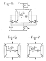
- transistors 13 and 14 take the place of the diodes 5 and 11 in Figure 4.
- the bases and emitters of these transistors 13 and 14 are connected between the output and the input of the respective operational amplifiers 4 and 10, in the same manner as the anode and cathode of the diodes 5 and 11 in Figure 4.
- the use of the transistors 13, 14 in place of the diodes 5, 11 provides the principal advantages that the operational amplifiers themselves no longer need to supply the current of one of the half-cycles, and that the rectified current can be converted via a resistor into a voltage, namely to V + , V- or both.
- Figures 6 and 7 show in heavier lines the path of the current during the negative and positive half-cycles respectively.
- Figure 8 shows a circuit corresponding to that shown in Figure 5, with a modified supply source.
- the latter consists of a series connection of two resistors 16 and 17, connected to the single voltage source.
- the connection point of the resistors 16 and 17 is connected to the connection point of the same polarity of the operational amplifiers 4 and 10.
- the voltage, which in Figure 5 is provided by the supply source 8, is supplied by way of the resistor 16.
- the circuit components lying within the box shown in broken lines may be in the form of an integrated circuit.
- a lower series resistor 9 can be used without the offset voltage having much effect on the output voltage U o .
- Figures 9 and 10 show in succession the output voltage U o through the resistor 7 for different input currents 1 1 .
- 1/n 1 is greater than
- Equation (10) will be further discussed below.
- a and D can be calculated from:
- the area E is:
Landscapes
- Engineering & Computer Science (AREA)
- Power Engineering (AREA)
- Physics & Mathematics (AREA)
- General Physics & Mathematics (AREA)
- Rectifiers (AREA)
- Measurement Of Current Or Voltage (AREA)
- Control Of Eletrric Generators (AREA)
Claims (4)
Priority Applications (1)
| Application Number | Priority Date | Filing Date | Title |
|---|---|---|---|
| AT84201361T ATE35490T1 (de) | 1983-09-28 | 1984-09-21 | Aktive doppelweg-gleichrichterschaltung. |
Applications Claiming Priority (2)
| Application Number | Priority Date | Filing Date | Title |
|---|---|---|---|
| NL8303319 | 1983-09-28 | ||
| NL8303319A NL8303319A (nl) | 1983-09-28 | 1983-09-28 | Aktieve dubbelzijdige gelijkrichtschakeling. |
Publications (2)
| Publication Number | Publication Date |
|---|---|
| EP0140418A1 EP0140418A1 (de) | 1985-05-08 |
| EP0140418B1 true EP0140418B1 (de) | 1988-06-29 |
Family
ID=19842462
Family Applications (1)
| Application Number | Title | Priority Date | Filing Date |
|---|---|---|---|
| EP84201361A Expired EP0140418B1 (de) | 1983-09-28 | 1984-09-21 | Aktive Doppelweg-Gleichrichterschaltung |
Country Status (5)
| Country | Link |
|---|---|
| US (1) | US4590547A (de) |
| EP (1) | EP0140418B1 (de) |
| AT (1) | ATE35490T1 (de) |
| DE (1) | DE3472515D1 (de) |
| NL (1) | NL8303319A (de) |
Families Citing this family (4)
| Publication number | Priority date | Publication date | Assignee | Title |
|---|---|---|---|---|
| US5510972A (en) * | 1994-06-29 | 1996-04-23 | Philips Electronics North America Corporation | Bridge rectifier circuit having active switches and an active control circuit |
| EP0870357B2 (de) * | 1995-12-29 | 2009-04-08 | EM Microelectronic-Marin SA | Aktiver gleichrichter mit minimalen energieverlusten |
| ATE300798T1 (de) * | 1998-09-18 | 2005-08-15 | Siemens Ag | Fehlerstromschutzeinrichtung mit bipolarer signalaufbereitung |
| EP1067667B1 (de) * | 1998-12-02 | 2006-03-01 | Seiko Epson Corporation | Stromversorgungsvorrichtung, stromversorgungsverfahren, tragbares elektronisches gerät und elektronisches uhrwerk |
Family Cites Families (5)
| Publication number | Priority date | Publication date | Assignee | Title |
|---|---|---|---|---|
| US3667028A (en) * | 1969-11-18 | 1972-05-30 | Dienes Honeywell Gmbh | Rectifier circuit including transistors |
| JPS5630961B2 (de) * | 1973-09-10 | 1981-07-18 | ||
| GB1491704A (en) * | 1974-05-21 | 1977-11-16 | Lucas Ltd Joseph | Full wave rectifiers |
| US4307305A (en) * | 1980-01-08 | 1981-12-22 | Northern Telecom, Inc. | Precision rectifier circuits |
| US4519024A (en) * | 1983-09-02 | 1985-05-21 | At&T Bell Laboratories | Two-terminal transistor rectifier circuit arrangement |
-
1983
- 1983-09-28 NL NL8303319A patent/NL8303319A/nl not_active Application Discontinuation
-
1984
- 1984-09-21 DE DE8484201361T patent/DE3472515D1/de not_active Expired
- 1984-09-21 EP EP84201361A patent/EP0140418B1/de not_active Expired
- 1984-09-21 AT AT84201361T patent/ATE35490T1/de active
- 1984-09-27 US US06/654,954 patent/US4590547A/en not_active Expired - Lifetime
Also Published As
| Publication number | Publication date |
|---|---|
| NL8303319A (nl) | 1985-04-16 |
| ATE35490T1 (de) | 1988-07-15 |
| EP0140418A1 (de) | 1985-05-08 |
| US4590547A (en) | 1986-05-20 |
| DE3472515D1 (de) | 1988-08-04 |
Similar Documents
| Publication | Publication Date | Title |
|---|---|---|
| US3327199A (en) | Transistorized high voltage regulated power supply system with temperature compensating means | |
| US3112449A (en) | Converter for converting alternating current signals to proportional constant polarity signals including compensating diode feedback | |
| US6664817B2 (en) | Zero-cross detection circuit | |
| EP0140418B1 (de) | Aktive Doppelweg-Gleichrichterschaltung | |
| US4670667A (en) | Series-connected power transistors | |
| US2696582A (en) | Phase sensitive rectifier | |
| US3297880A (en) | Electric circuits for supplying a substantially constant current to a load | |
| US3896366A (en) | D.c. to d.c. converter with conductive isolation | |
| JPS5875223A (ja) | 電源装置 | |
| US3274479A (en) | Rectifying apparatus for producing constant voltage | |
| JPS6091426A (ja) | 電源装置 | |
| US3258673A (en) | System for converting single phase | |
| US2780778A (en) | Phase sensitive strain gage amplifier rectifier circuit | |
| US3426283A (en) | Quadrature signal suppression circuit | |
| US3479583A (en) | Line voltage fluctuation insensitive detector for phase failures on three phase transformers | |
| US4196468A (en) | Series-type independent inverter | |
| SU1403299A1 (ru) | Стабилизированный преобразователь переменного напр жени в посто нное | |
| US3262047A (en) | Rectifying circuits using photoelectric devices | |
| US2940033A (en) | Circuit for sensing the highest phase voltage of a polyphase alternating current generator | |
| US3034074A (en) | Full-wave modulator circuits | |
| SU1566459A1 (ru) | Преобразователь переменного напр жени в посто нное | |
| US3546483A (en) | Control circuitry for a transformer supplied unidirectionally-conductive load | |
| SU980233A1 (ru) | Преобразователь переменного тока в посто нный | |
| US2553323A (en) | Voltage rectifier circuit | |
| US3522516A (en) | Power supply having incrementally related high voltage outputs |
Legal Events
| Date | Code | Title | Description |
|---|---|---|---|
| PUAI | Public reference made under article 153(3) epc to a published international application that has entered the european phase |
Free format text: ORIGINAL CODE: 0009012 |
|
| AK | Designated contracting states |
Designated state(s): AT BE CH DE FR GB IT LI LU NL SE |
|
| 17P | Request for examination filed |
Effective date: 19850809 |
|
| 17Q | First examination report despatched |
Effective date: 19860627 |
|
| R17C | First examination report despatched (corrected) |
Effective date: 19870127 |
|
| RAP1 | Party data changed (applicant data changed or rights of an application transferred) |
Owner name: HOLEC SYSTEMEN EN COMPONENTEN B.V. |
|
| GRAA | (expected) grant |
Free format text: ORIGINAL CODE: 0009210 |
|
| AK | Designated contracting states |
Kind code of ref document: B1 Designated state(s): AT BE CH DE FR GB IT LI LU NL SE |
|
| REF | Corresponds to: |
Ref document number: 35490 Country of ref document: AT Date of ref document: 19880715 Kind code of ref document: T |
|
| REF | Corresponds to: |
Ref document number: 3472515 Country of ref document: DE Date of ref document: 19880804 |
|
| ET | Fr: translation filed | ||
| ITF | It: translation for a ep patent filed | ||
| PLBE | No opposition filed within time limit |
Free format text: ORIGINAL CODE: 0009261 |
|
| STAA | Information on the status of an ep patent application or granted ep patent |
Free format text: STATUS: NO OPPOSITION FILED WITHIN TIME LIMIT |
|
| 26N | No opposition filed | ||
| ITTA | It: last paid annual fee | ||
| EPTA | Lu: last paid annual fee | ||
| EAL | Se: european patent in force in sweden |
Ref document number: 84201361.7 |
|
| REG | Reference to a national code |
Ref country code: CH Ref legal event code: NV Representative=s name: PATENTANWALTSBUREAU R. A. MASPOLI |
|
| REG | Reference to a national code |
Ref country code: CH Ref legal event code: PUE Owner name: HOLEC SYSTEMEN & COMPONENTEN B.V. TRANSFER- HOLEC |
|
| NLS | Nl: assignments of ep-patents |
Owner name: HOLEC HOLLAND N.V. |
|
| REG | Reference to a national code |
Ref country code: GB Ref legal event code: 732E |
|
| REG | Reference to a national code |
Ref country code: FR Ref legal event code: TP |
|
| PGFP | Annual fee paid to national office [announced via postgrant information from national office to epo] |
Ref country code: GB Payment date: 19990813 Year of fee payment: 16 |
|
| PGFP | Annual fee paid to national office [announced via postgrant information from national office to epo] |
Ref country code: CH Payment date: 19990816 Year of fee payment: 16 |
|
| PGFP | Annual fee paid to national office [announced via postgrant information from national office to epo] |
Ref country code: FR Payment date: 19990817 Year of fee payment: 16 |
|
| PGFP | Annual fee paid to national office [announced via postgrant information from national office to epo] |
Ref country code: NL Payment date: 19990819 Year of fee payment: 16 |
|
| PGFP | Annual fee paid to national office [announced via postgrant information from national office to epo] |
Ref country code: DE Payment date: 19990820 Year of fee payment: 16 |
|
| PGFP | Annual fee paid to national office [announced via postgrant information from national office to epo] |
Ref country code: SE Payment date: 19990823 Year of fee payment: 16 |
|
| PGFP | Annual fee paid to national office [announced via postgrant information from national office to epo] |
Ref country code: AT Payment date: 19990824 Year of fee payment: 16 |
|
| PGFP | Annual fee paid to national office [announced via postgrant information from national office to epo] |
Ref country code: LU Payment date: 19990826 Year of fee payment: 16 |
|
| PGFP | Annual fee paid to national office [announced via postgrant information from national office to epo] |
Ref country code: BE Payment date: 19990827 Year of fee payment: 16 |
|
| PG25 | Lapsed in a contracting state [announced via postgrant information from national office to epo] |
Ref country code: LU Free format text: LAPSE BECAUSE OF NON-PAYMENT OF DUE FEES Effective date: 20000921 Ref country code: GB Free format text: LAPSE BECAUSE OF NON-PAYMENT OF DUE FEES Effective date: 20000921 Ref country code: AT Free format text: LAPSE BECAUSE OF NON-PAYMENT OF DUE FEES Effective date: 20000921 |
|
| PG25 | Lapsed in a contracting state [announced via postgrant information from national office to epo] |
Ref country code: SE Free format text: THE PATENT HAS BEEN ANNULLED BY A DECISION OF A NATIONAL AUTHORITY Effective date: 20000929 |
|
| PG25 | Lapsed in a contracting state [announced via postgrant information from national office to epo] |
Ref country code: LI Free format text: LAPSE BECAUSE OF NON-PAYMENT OF DUE FEES Effective date: 20000930 Ref country code: CH Free format text: LAPSE BECAUSE OF NON-PAYMENT OF DUE FEES Effective date: 20000930 Ref country code: BE Free format text: LAPSE BECAUSE OF NON-PAYMENT OF DUE FEES Effective date: 20000930 |
|
| BERE | Be: lapsed |
Owner name: HOLEC HOLLAND N.V. Effective date: 20000930 |
|
| PG25 | Lapsed in a contracting state [announced via postgrant information from national office to epo] |
Ref country code: NL Free format text: LAPSE BECAUSE OF NON-PAYMENT OF DUE FEES Effective date: 20010401 |
|
| GBPC | Gb: european patent ceased through non-payment of renewal fee |
Effective date: 20000921 |
|
| REG | Reference to a national code |
Ref country code: CH Ref legal event code: PL |
|
| EUG | Se: european patent has lapsed |
Ref document number: 84201361.7 |
|
| PG25 | Lapsed in a contracting state [announced via postgrant information from national office to epo] |
Ref country code: FR Free format text: LAPSE BECAUSE OF NON-PAYMENT OF DUE FEES Effective date: 20010531 |
|
| NLV4 | Nl: lapsed or anulled due to non-payment of the annual fee |
Effective date: 20010401 |
|
| REG | Reference to a national code |
Ref country code: FR Ref legal event code: ST |
|
| PG25 | Lapsed in a contracting state [announced via postgrant information from national office to epo] |
Ref country code: DE Free format text: LAPSE BECAUSE OF NON-PAYMENT OF DUE FEES Effective date: 20010703 |