EP0140619A2 - Anisotrop elektrisch leitender Klebefilm und Verfahren zum Verbinden von Schaltungen unter dessen Anwendung - Google Patents
Anisotrop elektrisch leitender Klebefilm und Verfahren zum Verbinden von Schaltungen unter dessen Anwendung Download PDFInfo
- Publication number
- EP0140619A2 EP0140619A2 EP84306963A EP84306963A EP0140619A2 EP 0140619 A2 EP0140619 A2 EP 0140619A2 EP 84306963 A EP84306963 A EP 84306963A EP 84306963 A EP84306963 A EP 84306963A EP 0140619 A2 EP0140619 A2 EP 0140619A2
- Authority
- EP
- European Patent Office
- Prior art keywords
- adhesive film
- adhesive
- electroconductive
- particles
- film
- Prior art date
- Legal status (The legal status is an assumption and is not a legal conclusion. Google has not performed a legal analysis and makes no representation as to the accuracy of the status listed.)
- Granted
Links
Images
Classifications
-
- H—ELECTRICITY
- H10—SEMICONDUCTOR DEVICES; ELECTRIC SOLID-STATE DEVICES NOT OTHERWISE PROVIDED FOR
- H10W—GENERIC PACKAGES, INTERCONNECTIONS, CONNECTORS OR OTHER CONSTRUCTIONAL DETAILS OF DEVICES COVERED BY CLASS H10
- H10W70/00—Package substrates; Interposers; Redistribution layers [RDL]
- H10W70/60—Insulating or insulated package substrates; Interposers; Redistribution layers
- H10W70/62—Insulating or insulated package substrates; Interposers; Redistribution layers characterised by their interconnections
- H10W70/66—Conductive materials thereof
- H10W70/666—Organic materials or pastes
-
- H—ELECTRICITY
- H01—ELECTRIC ELEMENTS
- H01R—ELECTRICALLY-CONDUCTIVE CONNECTIONS; STRUCTURAL ASSOCIATIONS OF A PLURALITY OF MUTUALLY-INSULATED ELECTRICAL CONNECTING ELEMENTS; COUPLING DEVICES; CURRENT COLLECTORS
- H01R4/00—Electrically-conductive connections between two or more conductive members in direct contact, i.e. touching one another; Means for effecting or maintaining such contact; Electrically-conductive connections having two or more spaced connecting locations for conductors and using contact members penetrating insulation
- H01R4/04—Electrically-conductive connections between two or more conductive members in direct contact, i.e. touching one another; Means for effecting or maintaining such contact; Electrically-conductive connections having two or more spaced connecting locations for conductors and using contact members penetrating insulation using electrically conductive adhesives
-
- H—ELECTRICITY
- H05—ELECTRIC TECHNIQUES NOT OTHERWISE PROVIDED FOR
- H05K—PRINTED CIRCUITS; CASINGS OR CONSTRUCTIONAL DETAILS OF ELECTRIC APPARATUS; MANUFACTURE OF ASSEMBLAGES OF ELECTRICAL COMPONENTS
- H05K3/00—Apparatus or processes for manufacturing printed circuits
- H05K3/30—Assembling printed circuits with electric components, e.g. with resistors
- H05K3/32—Assembling printed circuits with electric components, e.g. with resistors electrically connecting electric components or wires to printed circuits
- H05K3/321—Assembling printed circuits with electric components, e.g. with resistors electrically connecting electric components or wires to printed circuits by conductive adhesives
- H05K3/323—Assembling printed circuits with electric components, e.g. with resistors electrically connecting electric components or wires to printed circuits by conductive adhesives by applying an anisotropic conductive adhesive layer over an array of pads
-
- H—ELECTRICITY
- H05—ELECTRIC TECHNIQUES NOT OTHERWISE PROVIDED FOR
- H05K—PRINTED CIRCUITS; CASINGS OR CONSTRUCTIONAL DETAILS OF ELECTRIC APPARATUS; MANUFACTURE OF ASSEMBLAGES OF ELECTRICAL COMPONENTS
- H05K2201/00—Indexing scheme relating to printed circuits covered by H05K1/00
- H05K2201/01—Dielectrics
- H05K2201/0104—Properties and characteristics in general
- H05K2201/0129—Thermoplastic polymer, e.g. auto-adhesive layer; Shaping of thermoplastic polymer
-
- H—ELECTRICITY
- H05—ELECTRIC TECHNIQUES NOT OTHERWISE PROVIDED FOR
- H05K—PRINTED CIRCUITS; CASINGS OR CONSTRUCTIONAL DETAILS OF ELECTRIC APPARATUS; MANUFACTURE OF ASSEMBLAGES OF ELECTRICAL COMPONENTS
- H05K2201/00—Indexing scheme relating to printed circuits covered by H05K1/00
- H05K2201/01—Dielectrics
- H05K2201/0104—Properties and characteristics in general
- H05K2201/0133—Elastomeric or compliant polymer
-
- H—ELECTRICITY
- H05—ELECTRIC TECHNIQUES NOT OTHERWISE PROVIDED FOR
- H05K—PRINTED CIRCUITS; CASINGS OR CONSTRUCTIONAL DETAILS OF ELECTRIC APPARATUS; MANUFACTURE OF ASSEMBLAGES OF ELECTRICAL COMPONENTS
- H05K2201/00—Indexing scheme relating to printed circuits covered by H05K1/00
- H05K2201/02—Fillers; Particles; Fibers; Reinforcement materials
- H05K2201/0203—Fillers and particles
- H05K2201/0263—Details about a collection of particles
- H05K2201/0266—Size distribution
-
- H—ELECTRICITY
- H05—ELECTRIC TECHNIQUES NOT OTHERWISE PROVIDED FOR
- H05K—PRINTED CIRCUITS; CASINGS OR CONSTRUCTIONAL DETAILS OF ELECTRIC APPARATUS; MANUFACTURE OF ASSEMBLAGES OF ELECTRICAL COMPONENTS
- H05K3/00—Apparatus or processes for manufacturing printed circuits
- H05K3/36—Assembling printed circuits with other printed circuits
- H05K3/361—Assembling flexible printed circuits with other printed circuits
Definitions
- the present invention relates to an anisotropic-electroconductive adhesive film which is electrically conductive only in the direction perpendicular to the surface thereof and not in any direction parallel to the surface.
- the invention also relates to a circuit connecting method employing such a film.
- Solders and electroconductive adhesives have so far been used widely as means of connecting large scale integrated circuits (LSI) or electrodes of liquid crystal display elements (LCD) to printed circuit boards and of bonding flexible flat cables (FFC) to external connecting terminals of various devices.
- LSI large scale integrated circuits
- LCD liquid crystal display elements
- FFC flexible flat cables
- soldering has a drawback of low reliability in adhesion due to hard and brittle properties thereof, that is, the liability of bonded parts to be readily separated by a shock or the like.
- Electroconductive adhesives are expensive because conductive fillers need to be incorporated to high concentrations of at least 20% by volume into adhesives in order to obtain necessary electric conductivity. Further drawbacks of conductive adhesives are that variation in the conductivity is caused by such a factor as the precipitation of the filler during storage or difficulty in uniform coating thereof and that environmental pollution due to the contained organic solvent may occur.
- the upper limit of the electroconductivity is 10° ⁇ -cm -1 , the appearance is black in color, and the transparency is lost completely, since carbon is used as the electroconductive filler.
- the bonding operation requires a long time ranging from 10 minutes to 10 hours and the workability is inferior, since the adhesion is achieved with Joule's heat.
- Adhesive tapes having electroconductive anisotropy are also known which are prepared by dispersing metal particles as electroconductive filler particles in a polymer binder (Japanese Patent Application Kokai (Laid-Open) No. 101040/76). Such adhesive tapes, however, are inferior in adhesive properties and transparency, since conductive fillers such as metal particles need to be incorporated in large quantities of at least 10% by volume in order to secure the necessary electroconductivity.
- connecting materials having anisotropic-electroconductivity which materials are produced by linear alignment of metal wires, carbon filaments, or carbon particles in polymers, for example, silicone rubber.
- these connecting materials have a number of drawbacks in that the minimum separation width of the conductors or insulators is as large as 0.2 mm at best, thus the use of these materials for connecting fine circuits is limited, compression pressure should always be applied in order to maintain the connection in a good state and this requires a special fixing means, which results in restricting equipment designs, and the materials themselves are opaque so that the adjustment of relative positions of circuits is complicated when the circuits are superposed and connected together.
- an object of the present invention is to provide an anisotropic-electroconductive adhesive film which permits achieving with simple operation the electroconductive connection between two groups of connecting terminals which face each other and are each aligned at fine pitches.
- Another object of the invention is to provide a method for connecting circuits by using said film.
- an anisotropic-electroconductive adhesive film comprising an adhesive component and electroconductive particles, characterized in that the adhesive component contains 0.1 to 10% by volume of electroconductive particles having an average particle size of 1 to 50 lim with a ratio of the minimum diameter to the maximum diameter of each particle being 0.5 to 1.0, and the thickness of an adhesive layer is at least 110% of the average particle size of the electroconductive particles and not more than 100 ⁇ m.
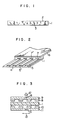
- Fig. 1 is a cross-sectional view of the anisotropic-electroconductive adhesive film according to the invention
- Fig. 2 is a perspective view showing the connected state of a group of connecting terminals formed on a circuit board
- Fig. 3 is a schematic cross-sectional view showing the concept of the connecting operations.
- Fig. 1 shows the fundamental construction of the anisotropic-electroconductive adhesive film according to the invention.
- the adhesive film comprises an adhesive layer 2 of bonding material and electroconductive particles 3 dispersed therein.
- the adhesive layer 2 is an electrical insulator and has functions of holding electroconductive particles 3 with dispersed state and adhering a printed circuit board or the like.
- the layer 2 undergoes plastic deformation on applying pressure with or without heating, and this brings electroconductive particles into contact one with another along the direction of the pressure application so as to maintain electric conductivity permanently.
- Fig. 2 shows the state wherein a connecting terminal 5 of a flexible printed circuit board 4 is connected electrically with a connecting terminal 7 of a flexible flat cable 6 by using such an adhesive film as shown in Fig. 1.
- the opposing pairs of connecting terminals 5-7, 5'-7', ... are each in an electrically conductive state while the communications between the neighboring terminals 5 and 5', ... and between the neighboring terminals 7 and 7', ... are each in an electrically insulated state.
- the adhesive film according to the invention has an anisotropy in electrical conductivity between the directions perpendicular and parallel to the surface'thereof (hereinafter for convenience, the direction perpendicular to the film surface is referred to as the "thickness direction" and the directions parallel to the film surface as the "plane direction".
- the film has a resistivity of at least 10 6 Q-cm in the plane direction and a resistivity of not more than 10 3 Q-cm in the thickness direction, exhibiting thus a great anisotropy in resistivity.
- the adhesive film has a small minimum separation width of resistance both in the plane and the thickness direction, thus being good in resolution. That is, the minimum insulation width in the film plane direction is 0.05 mm.
- the application of the film can be accomplished under both heat-sensitive and pressure-sensitive conditions. Accordingly, the adhesive film offers good application workability and strong adhesion as well as high electrical conductivity and additionally has a considerably high transparency.
- the above-mentioned features of the film are due to the high anisotropic electrical conductivity that has become obtainable by the incorporation of special electroconductive particles in small amounts and due to the arbitrary compounding enabled thereby for the film formation.
- the shape of the electroconductive particles is the main cause of the fact that the film exhibits a high anisotropic conductivity with small amounts of electroconductive particles.
- the adhesive layer in application becomes fluid with heat or pressure and each electroconductive particle embedded in the surface layer of the film will be in one- point contact with the surface of the conductor to be bonded, so that the adhesive film sufficiently adapts itself to the adhesion surface of the conductor and provides high bond strength.
- Electroconductive particles in the surface layer take such configurations as to readily contact with electroconductive particles present on the deeper side, forming links in the thickness direction and as to have a little opportunity to contact with other electroconductive particles in the plane direction, whereby the anisotropic conductivity is obtained.
- the electroconductive particles used in the invention are metallic particles of 1 to 50 ⁇ m in diameter.
- the ratio of the smallest diameter to the largest diameter of each particle is 0.5 to 1.0.
- the particles are contained in the adhesive component in an amount of 0.1 to 10% by volume.
- the maximum particle size is desirably 1 to 50 ⁇ m, more preferably 1 to 10 ⁇ m. When it is less than 1 ⁇ m, a larger amount of electroconductive particles are required, which results in deteriorating the bond strength greatly.
- the maximum particle size is more than 50 ⁇ m, it is impossible to obtain a smooth adhesive surface having good affinity to an adherend from the viewpoint of thickness of the adhesive film layer, which results in failing to give sufficient adhesiveness. Further, insulating properties and resolution properties at electric conduction are also undesirably worsened.
- the ratio of the smallest diameter to the largest of each particle (hereinafter referred to as "the aspect ratio") is about 0.5 to 1.0 as stated above. If the aspect ratio is out of the above range, the balance between the electroconductivity and the adhesiveness will be disturbed.
- a typical example of the particle shapes satisfying the above condition is spherical or nearly spherical. However, the shape is not particularly limited so long as the aspect ratio falls in the above range. The particles are allowed to have projections or depressions on the surface.
- the particle size herein means the average diameter of all the particles.
- the shape and diameter of the particles are conveniently measured by way of, for example, an electron microscope.
- the adhesive layer is fluidized by the heating or pressure at the time of adhesion, which results in making it possible to contact one point of the special particles with the conductor surface.
- flaky conductive particles for example, are aligned with longer axes thereof being directed in parallel to the adhesive surface in the steady state and the adherend surface is therefore occupied mostly with the electroconductive particles, thereby the adhesive properties are lowered to a large extent.
- the electroconductive particles can be produced by any possible method from the following materials: Metals, for example, Ni, Fe, Cr, Co, Al,,Sb, Mo, Cu, Ag, Pt, and Au, and alloys and oxides of these metals.
- Metals for example, Ni, Fe, Cr, Co, Al,,Sb, Mo, Cu, Ag, Pt, and Au, and alloys and oxides of these metals.
- the above materials may be used alone or in combination.
- metal-coated particles of non-conductive materials for example, glass and plastics.
- Suitable content of conductive particles in the adhesive component layer is 0.1 to 10% by volume.
- the thickness of the adhesive film is at least 110% of the average particle size of the electroconductive particles contained and desirably not more than 100 ⁇ m. With the particle content less than 0.1% by volume, no satisfactory electrical conductivity is obtained, and when the content exceeds 10% by volume, the bond strength much lowers and no sufficient transparency of the film is obtainable.
- the polymer used for the adhesive some considerations are necessary depending upon the method of applying the adhesive film, in other words, depending upon whether the film is of heat sensitive type or of pressure sensitive type.
- the heat sensitive type of adhesive film is applied by heating to soften and flow on the adherend surface, thereby bonding the object.
- a polymer relatively hard at ordinary temperatures is used for the film of heat sensitive type.
- the pressure sensitive type of adhesive film which is applied with pressure on an adherend, is relatively soft to such an extent that stickiness thereof is perceptible even at ordinary temperatures.
- thermoplastic polymers that exhibit plasticity on heating are usually employed as a main component.
- These polymers include, for example, an ethylene-vinyl acetate copolymer, polyethylene, ethylene-propylene copolymer, ethylene-acrylate copolymer, acrylic rubber, polyisobutylene, atactic polypropylene, poly(vinyl butyral), styrene-butadiene copolymer, polybutadiene, ethyl-cellulose, polyamide, and polyurethane. These polymers may be used alone or as a mixture thereof.
- polymers exhibiting stickiness even at ordinary temperatures can be employed. These polymers include an acrylic rubber, natural rubber, silicone rubber, polychloroprene, butadiene-styrene copolymer, ethylene-vinyl acetate copolymer, polyisobutylene, and poly(vinyl ether) rubber. These polymers also may be used alone or as a mixture thereof.
- tackifiers and conventional additives such as plasticizers, crosslinking agents, and antioxidants can be used, if necessary, for either the heat sensitive type or the pressure sensitive type.
- Suitable tackifiers for use herein include, for example, rosin family resins such as rosin, hydro-rosin, ester gum, and maleic acid-modified rosin, petroleum resin, xylene resin, and cumarone-indene resin. These tackifiers may be used alone or as a mixture thereof.
- an electroconductive adhesive composition is obtained.
- a surfactant for example, can be used, if required, as a dispersing agent for the electroconductive particles.
- the above electroconductive adhesive composition can be coated on paper, plastic film, or the like, which is coated with a separator if necessary for helping the later separation of the adhesive film, by means of a roll coater or the like, followed by drying, or by hot melt coating to give an electroconductive adhesive film.
- the adhesive layer alone without using such a separator can be wound up into a roll or folded u p .
- the thickness of the adhesive film is decided by considering the relation to the diameter of the electroconductive particles used and characteristics of the film.
- the thickness needs to be at least 110% of the particle size of the electroconductive particles in order to hold the particles satisfactorily in the adhesive. If the thickness is less than 110%, some of the electroconductive particles will be protected not completely with the adhesive, and in consequence will be oxidized or corroded, thereby the electrical conductivity being deteriorated. Also from the viewpoint of characteristics of the adhesive film, the thickness is required in the range of preferably 5 to 100 ⁇ m, particularly preferably 5 to 50 ⁇ m. When the thickness is less than 5 ⁇ m, no sufficient adhesiveness is obtained, and the thickness more than 100 ⁇ m is impractical since a large amount of electroconductive particles need to be mixed in order to secure sufficient electrical conductivity with such a thick film.
- One or both sides of the formed adhesive film may be covered with separator films if necessary for the purpose of protecting from the adherence of dust or the like.
- the adhesive film when both sides thereof are covered with separator films, can be continuously wound up into a roll or folded up.
- the thus obtained adhesive film has good transparency.
- Transparent adhesive films are advantageous in that quality control in the production process is easy to practice in the assembly of display devices or the like, such structures thereof can be designed that the objects to bond can be seen through in bonding operations, and the adjustment of relative positions (hereinafter this adjustment is referred to as registration) for bonding circuits is facilitated and thereby the film application can be automated.
- the film is preliminarily attached onto all the surfaces of connecting terminals on an adherent A, a separator, if present on the film, is peeled off, the connecting terminals on the other adherend B are placed on the film face to face, and the bonding is accomplished with a hot press or heat roll.
- the anisotropic-electroconductive film according to the invention has a total light transmittance of at least 40% as measured in accordance with JIS K-6714. This is favorable since optical registration of the portions to be bonded together is possible when at least one of the circuit boards is a flexible printed circuit board that comprises a circuit formed on a transparent film.
- Fig. 3 denotes an anisotropic-electroconductive adhesive film according to the invention which is interposed between the upper circuit board 9 having connecting terminals 8 and the lower circuit board 11 having connecting terminals 10.
- a light source 12 a usual electric lamp or fluorescent lamp can be used, preferably provided with a condenser, but the particularly preferred light source is a laser from the viewpoint of lineality of light.
- the base materials of the circuit board 9 and 10 are preferably both transparent, at least the circuit board 9 on the light source 12 side is required to be transparent.
- the registration can also be accomplished by recording marks 14 and 15 for registration on the boards 9 and 11, respectively, and utilizing light from the light source 12.
- the registration can be accomplished by moving the circuit board 11 by the driving means 13 provided with a photosensor so that the reflected light signal will be in accordance with the connecting terminals 8.
- a metal plate (SUS-430BA, 500 ⁇ m thick) and a copper foil 35 ⁇ m thick were bonded together with each adhesive film thus obtained. That is, each adhesive film was applied on one SUS-430BA sheet, the separator film was peeled off, and one copper foil was bonded onto the stripped surface of the adhesive by using a pair of heat rolls (heated to 120°C). Properties of the films and results of the bonding are shown in Table 1.
- An adhesive film was prepared in the same manner as in Examples 1 and 2 except that the content of the electroconductive particle was increased to 20% by volume.
- the adhesiveness was by far inferior though the conductivity was good.
- the total light transmittance of the adhesive film was 20% and the low clarity was also ascertained by visual observation.
- Adhesive films were prepared by following the procedure of Examples 1 and 2, but the materials used and the thickness of the coats were varied and the coating was carried out by means of a hot-melt applicator (without using any solvent).
- a styrene-butadiene block copolymer (mfd. by Asahi Chemical Industry Co., Ltd. under the tradename of Toughprene A, hereinafter designated as SBR; MI 2.6) and an aromatic tackifier (mfd. by Mitsui Petrochemical Industries Co., Ltd., tradename, Petrosin #150; softening point 150°C) were employed.
- SBR styrene-butadiene block copolymer
- MI 2.6 aromatic tackifier
- the compounding ratio of the SBR to the tackifier was 100 parts : 50 parts.
- the conductive particle used was a nickel powder (supplied by International Nickel Co. under the tradename of Carbonyl 123; spherical shape, average particle size 4.5 ⁇ m, fine projections and depressions were present throughout the surface, aspect ratio 0.70).
- the SBR and the tackifier (the above compounding ratio) were fed into a melt mixer attached to the hot-melt applicator and were melted by heating. Said conductive particle was added to the melt, and coating films of different thicknesses were prepared.
- the evaluation of the thus prepared adhesive films was conducted in the same manner as in Examples 1 and 2 except that the application of films for bonding was carried out with a hot press (temperature of object: 160°C, pressure 2 kg/cm 2 , press time 5 seconds). All the obtained adhesive films showed considerably high transparency.
- the resistivities in the plane direction were higher by several orders than those in the thickness direction, showing high anisotropy in electroconductivity.
- An adhesive film was prepared in the same manner as in Examples 3 to 5 except that the thickness of the coat was made 150 ⁇ m.
- the resistivity in the thickness direction was as high as 10 8 ⁇ -cm.
- the adhesive film showed considerably low transparency.
- An adhesive film was prepared by following the procedure of Example 4 but using a flaky nickel powder (thickness 0.6 ⁇ m, largest diameter ca. 40 ⁇ m, aspect ratio 0.015).
- the film showed a very low adhesive strength and a nearly isotropic electroconductivity.
- this mixture was applied on a separator film of 100 ⁇ m in total thickness which had been prepared by coating a glassine paper substrate with a polyethylene layer and treating the surface of the polyethylene layer with a silicone.
- the coated separator was dried, giving an adhesive film 40 ⁇ m thick.
- the adhesive film showed high stickiness at room temperature and could be applied with simple operation.
- the resulting resistivity in the thickness direction was as low as 10-2 ⁇ -cm.
- the adhesive film was considerably transparent, that is, the total light transmittance was 70%.
- the film showed high stickiness and could be applied simply at room temperature by using a pair of rubber rolls.
- the resulting resistivity in the thickness direction was as low as 10 -3 ⁇ -cm, and the transparency was sufficient for practical use.
- crosslinking agent incorporated into the adhesive gave high cohesion, that is, high heat resistance to the adhesive film.
- Adhesive strength The 180°-degree peeling method in accordance with JIS Z-0237 was applied. The measurement was conducted at a peeling speed 50 mm/min., 20°C, and 65% RH by using a copper foil bent by 90° degree.
- Total light transmittance This was measured in accordance with JIS K-6714 using a digital turbidimeter (Model NDH-20D of Nippon Denshoku Kogyo K.K.).
- Example 2 The same ethylene-vinyl acetate copolymer and the same rosin-base tackifier (softening point 70°C) as used in Example 1 were dissolved in equal amounts in toluene to prepare solutions of concentration 20%.
- a nickel powder (particle shape: spherical, average particle size:4.5 ⁇ m, aspect ratio: 0.70) having fine projections and depressions was mixed in the proportions shown in Table 2 with the above solutions. The mixtures were each ball-milled for 24 hours to give adhesive compounded liquids.
- Each compounded liquid was applied on a 25-pm thick polyester film surface-treated with a releasing agent by means of a bar coater so as to give a dry thickness of 30 ⁇ m, and was dried at 120°C for 3 minutes to remove the toluene.
- adhesive films of different conductive particle contents were obtained.
- two flexible polyester circuit boards pitch of circuit lines: 0.1 mm, line width 0.05 mm
- these films were found to have considerably high transparency, that is, the total light transmittance was 40% or more, since contents of the conductive particles were low.
- An adhesive film was prepared in the same manner as in Example 10 but using a flaky nickel powder (particle shape: flaky, thickness 0.6 ⁇ m, largest diameter ca. 40 ⁇ m, aspect ratio 0.015).
- the film showed a very low bond strength and a nearly isotropic electroconductivity.
- this mixture was applied on a separator film of 100 ⁇ m in total thickness which had been prepared by coating a glassine paper substrate with a polyethylene layer and treating the surface of the polyethylene layer with a silicone.
- the coated separator was dried, giving an adhesive film 20 ⁇ m thick.
- the adhesive film showed high stickiness at room temperature and could be applied with simple operation.
- the resulting resistivity in the thickness direction was as low as 10 -1 ⁇ -cm.
- the adhesive film was considerably transparent, that is, the total light transmittance was 70%.
- An adhesive compound composed of 100 parts of an acrylic polymer and of 1 part of an isocyanate type crosslinking agent was mixed with 10% by volume of a silver powder (particle shape: spherical, particle size 0.5 ⁇ m, aspect ratio 0.9). From this mixture, an adhesive film 10 ⁇ m thick was prepared and evaluated in the same manner as in Example 12.
- the film showed high stickiness and could be applied simply at room temperature by using a pair of rubber rolls.
- the resulting resistivity in the thickness direction was 10 -3 ⁇ -cm, and the transparency was sufficient for practical use.
- crosslinking agent incorporated into the adhesive gave high cohesion, that is, high heat resistance to the adhesive film.
- the anisotropic-electroconductive adhesive film according to the present invention exhibits sufficient anisotropic electroconductivity due to a specified electroconductive particle mixed and has high bond strength since the content of the particle is as low as 0.1 to 10% by volume.
- the adhesive film is available in sheet or film form, a stable electrical conductivity can be constantly obtained, bonding operation therewith is simple and can be completed in a short time, thus a considerable reduction in process time being possible. Moreover, there is no hazard of environmental pollution since bonding operation with this film is feasible without using any solvent. Furthermore, this film has good transparency due to the low content of the electroconductive particle. Accordingly, connection of circuits can be carried out by an optical means with this film and therefore accurate registration of circuits is possible. Having anisotropic electroconductivity, this film can be applied to fine circuits, and the bonding function of the film enables the bonding and fixing of circuits simultaneously with the registration. This makes possible automatic connection of circuits, and thus the improvement of the registration accuracy and much labor saving will become possible.
Landscapes
- Engineering & Computer Science (AREA)
- Manufacturing & Machinery (AREA)
- Microelectronics & Electronic Packaging (AREA)
- Adhesives Or Adhesive Processes (AREA)
- Adhesive Tapes (AREA)
- Non-Insulated Conductors (AREA)
Applications Claiming Priority (6)
| Application Number | Priority Date | Filing Date | Title |
|---|---|---|---|
| JP19323783A JPS6084718A (ja) | 1983-10-14 | 1983-10-14 | 導電異方性接着シ−ト |
| JP193237/83 | 1983-10-14 | ||
| JP223954/83 | 1983-11-28 | ||
| JP22395483A JPS60117572A (ja) | 1983-11-28 | 1983-11-28 | 回路の接続方法 |
| JP58236883A JPS60130004A (ja) | 1983-12-15 | 1983-12-15 | 透明導電異方性接着シ−ト |
| JP236883/83 | 1983-12-15 |
Publications (3)
| Publication Number | Publication Date |
|---|---|
| EP0140619A2 true EP0140619A2 (de) | 1985-05-08 |
| EP0140619A3 EP0140619A3 (en) | 1986-05-14 |
| EP0140619B1 EP0140619B1 (de) | 1993-03-17 |
Family
ID=27326730
Family Applications (1)
| Application Number | Title | Priority Date | Filing Date |
|---|---|---|---|
| EP84306963A Expired - Lifetime EP0140619B1 (de) | 1983-10-14 | 1984-10-11 | Anisotrop elektrisch leitender Klebefilm und Verfahren zum Verbinden von Schaltungen unter dessen Anwendung |
Country Status (2)
| Country | Link |
|---|---|
| EP (1) | EP0140619B1 (de) |
| DE (1) | DE3486101T2 (de) |
Cited By (13)
| Publication number | Priority date | Publication date | Assignee | Title |
|---|---|---|---|---|
| EP0195859A3 (de) * | 1985-03-27 | 1987-09-16 | Norwood Industries, Inc. | Leitungsfähige Klebstoffe |
| EP0242025A1 (de) * | 1986-02-14 | 1987-10-21 | Hitachi Chemical Co., Ltd. | Anisotrope elektrizitätsleitende Klebstoffzusammensetzung, Verfahren zum Verbinden von Stromkreisen und die so erhaltenen Stromkreise |
| US4729809A (en) * | 1985-03-14 | 1988-03-08 | Amp Incorporated | Anisotropically conductive adhesive composition |
| EP0261527A3 (de) * | 1986-09-25 | 1989-04-26 | Tektronix Inc. | Gerät und Verfahren zur Herstellung einer hohen Dichte bei elektrischen Zwischenverbindungen |
| EP0397304A1 (de) * | 1989-03-15 | 1990-11-14 | Sharp Kabushiki Kaisha | Verfahren und Anordnung zur Leitungsverbindung für eine Anzeigevorrichtung |
| US5129143A (en) * | 1982-11-29 | 1992-07-14 | Amp Incorporated | Durable plating for electrical contact terminals |
| FR2712133A1 (fr) * | 1993-11-03 | 1995-05-12 | Isa France Sa | Connecteur flexible thermocollable. |
| WO2000001782A1 (de) * | 1998-07-04 | 2000-01-13 | Beiersdorf Ag | Elektrisch leitfähige, thermoplastische und hitzeaktivierbare klebstofffolie |
| EP1002844A3 (de) * | 1998-11-21 | 2000-10-11 | Beiersdorf Aktiengesellschaft | Elektrisch leitfähige, thermoplastische und hitzeaktivierbare Klebstofffolie |
| WO2008024441A3 (en) * | 2006-08-23 | 2008-05-22 | Molex Inc | Relay connector for fpc using adhesive |
| DE102008034946A1 (de) * | 2008-07-26 | 2010-01-28 | Semikron Elektronik Gmbh & Co. Kg | Edelmetallverbindungsmittel sowie Herstellungs- und Verwendungsverfahren hierzu |
| CN112421262A (zh) * | 2014-11-17 | 2021-02-26 | 迪睿合株式会社 | 各向异性导电膜、连接结构体及其制造方法 |
| US20210298181A1 (en) * | 2020-03-17 | 2021-09-23 | Innolux Corporation | Electronic device |
Family Cites Families (4)
| Publication number | Priority date | Publication date | Assignee | Title |
|---|---|---|---|---|
| US3896544A (en) * | 1973-01-15 | 1975-07-29 | Essex International Inc | Method of making resilient electrical contact assembly for semiconductor devices |
| US4098945A (en) * | 1973-07-30 | 1978-07-04 | Minnesota Mining And Manufacturing Company | Soft conductive materials |
| GB1476571A (en) * | 1974-06-17 | 1977-06-16 | Chomerics Inc | Electrical connector |
| GB2047476B (en) * | 1979-02-26 | 1983-06-15 | Secr Defence | Applying circuit elements to a substrate |
-
1984
- 1984-10-11 EP EP84306963A patent/EP0140619B1/de not_active Expired - Lifetime
- 1984-10-11 DE DE8484306963T patent/DE3486101T2/de not_active Expired - Lifetime
Cited By (20)
| Publication number | Priority date | Publication date | Assignee | Title |
|---|---|---|---|---|
| US5129143A (en) * | 1982-11-29 | 1992-07-14 | Amp Incorporated | Durable plating for electrical contact terminals |
| US4729809A (en) * | 1985-03-14 | 1988-03-08 | Amp Incorporated | Anisotropically conductive adhesive composition |
| EP0195859A3 (de) * | 1985-03-27 | 1987-09-16 | Norwood Industries, Inc. | Leitungsfähige Klebstoffe |
| EP0242025A1 (de) * | 1986-02-14 | 1987-10-21 | Hitachi Chemical Co., Ltd. | Anisotrope elektrizitätsleitende Klebstoffzusammensetzung, Verfahren zum Verbinden von Stromkreisen und die so erhaltenen Stromkreise |
| US4740657A (en) * | 1986-02-14 | 1988-04-26 | Hitachi, Chemical Company, Ltd | Anisotropic-electroconductive adhesive composition, method for connecting circuits using the same, and connected circuit structure thus obtained |
| EP0261527A3 (de) * | 1986-09-25 | 1989-04-26 | Tektronix Inc. | Gerät und Verfahren zur Herstellung einer hohen Dichte bei elektrischen Zwischenverbindungen |
| EP0397304A1 (de) * | 1989-03-15 | 1990-11-14 | Sharp Kabushiki Kaisha | Verfahren und Anordnung zur Leitungsverbindung für eine Anzeigevorrichtung |
| US5112262A (en) * | 1989-03-15 | 1992-05-12 | Sharp Kabushiki Kaisha | Apparatus and method for electrical connections of a display device |
| FR2712133A1 (fr) * | 1993-11-03 | 1995-05-12 | Isa France Sa | Connecteur flexible thermocollable. |
| US6861138B1 (en) | 1998-07-04 | 2005-03-01 | Tesa Ag | Electrically conductive, thermoplastic, heat-activated adhesive film |
| WO2000001782A1 (de) * | 1998-07-04 | 2000-01-13 | Beiersdorf Ag | Elektrisch leitfähige, thermoplastische und hitzeaktivierbare klebstofffolie |
| EP1002844A3 (de) * | 1998-11-21 | 2000-10-11 | Beiersdorf Aktiengesellschaft | Elektrisch leitfähige, thermoplastische und hitzeaktivierbare Klebstofffolie |
| WO2008024441A3 (en) * | 2006-08-23 | 2008-05-22 | Molex Inc | Relay connector for fpc using adhesive |
| CN101529660B (zh) * | 2006-08-23 | 2012-07-04 | 莫列斯公司 | 使用粘合剂的fpc中继连接器 |
| DE102008034946A1 (de) * | 2008-07-26 | 2010-01-28 | Semikron Elektronik Gmbh & Co. Kg | Edelmetallverbindungsmittel sowie Herstellungs- und Verwendungsverfahren hierzu |
| DE102008034946B4 (de) * | 2008-07-26 | 2016-05-19 | Semikron Elektronik Gmbh & Co. Kg | Herstellungsverfahren eines Edelmetallverbindungsmittels |
| CN112421262A (zh) * | 2014-11-17 | 2021-02-26 | 迪睿合株式会社 | 各向异性导电膜、连接结构体及其制造方法 |
| US20210298181A1 (en) * | 2020-03-17 | 2021-09-23 | Innolux Corporation | Electronic device |
| US11510321B2 (en) * | 2020-03-17 | 2022-11-22 | Innolux Corporation | Electronic device |
| US12309940B2 (en) | 2020-03-17 | 2025-05-20 | Innolux Corporation | Electronic device |
Also Published As
| Publication number | Publication date |
|---|---|
| DE3486101T2 (de) | 1993-07-01 |
| EP0140619A3 (en) | 1986-05-14 |
| EP0140619B1 (de) | 1993-03-17 |
| DE3486101D1 (de) | 1993-04-22 |
Similar Documents
| Publication | Publication Date | Title |
|---|---|---|
| US4731282A (en) | Anisotropic-electroconductive adhesive film | |
| CA1220252A (en) | Adhesive electrical interconnecting means | |
| EP0140619B1 (de) | Anisotrop elektrisch leitender Klebefilm und Verfahren zum Verbinden von Schaltungen unter dessen Anwendung | |
| CA1220251A (en) | Electrical interconnection means | |
| US4595606A (en) | Solderable conductive compositions having high adhesive strength | |
| US3762946A (en) | Small particle loaded electrically conductive adhesive tape | |
| US4868637A (en) | Electronic device including uniaxial conductive adhesive and method of making same | |
| US5084211A (en) | Anisotropically electroconductive adhesive | |
| US4595605A (en) | Solderable conductive compositions that are capable of being soldered by non silver-bearing solder and that can be bonded directly to substrates and which are flexible | |
| JPS6143644A (ja) | はんだ付けができ、柔軟性で、かつ基材に接着可能な伝導性組成物、その調製方法および用途 | |
| US4720740A (en) | Electronic device including uniaxial conductive adhesive and method of making same | |
| JPS6177278A (ja) | 回路の接続部材 | |
| EP0501270A1 (de) | Elektronische Vorrichtung mit uniaxial leitfähiger Klebezusammensetzung | |
| JPS6177279A (ja) | 回路の接続部材 | |
| JP3542874B2 (ja) | 導電性微粒子 | |
| JPH0773066B2 (ja) | 回路の接続部材 | |
| JP2644717B2 (ja) | シート状異方導電性接着剤 | |
| JPS6178069A (ja) | 回路の接続部材 | |
| EP0083503B1 (de) | Isoliertes Verbindungsblatt | |
| KR920005071B1 (ko) | 배선기판 | |
| JPH03126783A (ja) | 異方導電性接着フイルム | |
| JPH01249880A (ja) | 異方導電性接着シート | |
| TW201936845A (zh) | 導電性接著劑組成物 | |
| JPH06215633A (ja) | 接続部材 | |
| JPS60117504A (ja) | 高電流回路接続用導電異方性接着シ−ト |
Legal Events
| Date | Code | Title | Description |
|---|---|---|---|
| PUAI | Public reference made under article 153(3) epc to a published international application that has entered the european phase |
Free format text: ORIGINAL CODE: 0009012 |
|
| AK | Designated contracting states |
Designated state(s): DE GB |
|
| PUAL | Search report despatched |
Free format text: ORIGINAL CODE: 0009013 |
|
| AK | Designated contracting states |
Kind code of ref document: A3 Designated state(s): DE GB |
|
| 17P | Request for examination filed |
Effective date: 19861003 |
|
| 17Q | First examination report despatched |
Effective date: 19880422 |
|
| GRAA | (expected) grant |
Free format text: ORIGINAL CODE: 0009210 |
|
| AK | Designated contracting states |
Kind code of ref document: B1 Designated state(s): DE GB |
|
| REF | Corresponds to: |
Ref document number: 3486101 Country of ref document: DE Date of ref document: 19930422 |
|
| PLBE | No opposition filed within time limit |
Free format text: ORIGINAL CODE: 0009261 |
|
| STAA | Information on the status of an ep patent application or granted ep patent |
Free format text: STATUS: NO OPPOSITION FILED WITHIN TIME LIMIT |
|
| 26N | No opposition filed | ||
| REG | Reference to a national code |
Ref country code: GB Ref legal event code: IF02 |
|
| PGFP | Annual fee paid to national office [announced via postgrant information from national office to epo] |
Ref country code: GB Payment date: 20031008 Year of fee payment: 20 |
|
| PGFP | Annual fee paid to national office [announced via postgrant information from national office to epo] |
Ref country code: DE Payment date: 20031023 Year of fee payment: 20 |
|
| PG25 | Lapsed in a contracting state [announced via postgrant information from national office to epo] |
Ref country code: GB Free format text: LAPSE BECAUSE OF EXPIRATION OF PROTECTION Effective date: 20041010 |
|
| REG | Reference to a national code |
Ref country code: GB Ref legal event code: PE20 |
|
| APAH | Appeal reference modified |
Free format text: ORIGINAL CODE: EPIDOSCREFNO |