EP0140645A2 - Semiconductor light-emitting device - Google Patents
Semiconductor light-emitting device Download PDFInfo
- Publication number
- EP0140645A2 EP0140645A2 EP84307115A EP84307115A EP0140645A2 EP 0140645 A2 EP0140645 A2 EP 0140645A2 EP 84307115 A EP84307115 A EP 84307115A EP 84307115 A EP84307115 A EP 84307115A EP 0140645 A2 EP0140645 A2 EP 0140645A2
- Authority
- EP
- European Patent Office
- Prior art keywords
- active layer
- layer
- emitting device
- undoped
- light
- Prior art date
- Legal status (The legal status is an assumption and is not a legal conclusion. Google has not performed a legal analysis and makes no representation as to the accuracy of the status listed.)
- Granted
Links
- 239000004065 semiconductor Substances 0.000 title claims abstract description 22
- 239000002019 doping agent Substances 0.000 claims description 18
- 229910052793 cadmium Inorganic materials 0.000 claims description 5
- 238000001228 spectrum Methods 0.000 abstract description 9
- 239000013078 crystal Substances 0.000 description 10
- 238000009792 diffusion process Methods 0.000 description 10
- 239000000969 carrier Substances 0.000 description 6
- 239000000758 substrate Substances 0.000 description 6
- 230000005540 biological transmission Effects 0.000 description 3
- 238000010586 diagram Methods 0.000 description 3
- 239000012535 impurity Substances 0.000 description 3
- 238000000034 method Methods 0.000 description 3
- 230000003287 optical effect Effects 0.000 description 3
- 230000001419 dependent effect Effects 0.000 description 2
- 239000000835 fiber Substances 0.000 description 2
- 239000000463 material Substances 0.000 description 2
- 239000010453 quartz Substances 0.000 description 2
- VYPSYNLAJGMNEJ-UHFFFAOYSA-N silicon dioxide Inorganic materials O=[Si]=O VYPSYNLAJGMNEJ-UHFFFAOYSA-N 0.000 description 2
- 229910005542 GaSb Inorganic materials 0.000 description 1
- -1 at a high density Substances 0.000 description 1
- WPYVAWXEWQSOGY-UHFFFAOYSA-N indium antimonide Chemical compound [Sb]#[In] WPYVAWXEWQSOGY-UHFFFAOYSA-N 0.000 description 1
- 239000007791 liquid phase Substances 0.000 description 1
- 238000004519 manufacturing process Methods 0.000 description 1
- 239000002184 metal Substances 0.000 description 1
- 229910052751 metal Inorganic materials 0.000 description 1
- 229910052718 tin Inorganic materials 0.000 description 1
Images


Classifications
-
- H—ELECTRICITY
- H10—SEMICONDUCTOR DEVICES; ELECTRIC SOLID-STATE DEVICES NOT OTHERWISE PROVIDED FOR
- H10H—INORGANIC LIGHT-EMITTING SEMICONDUCTOR DEVICES HAVING POTENTIAL BARRIERS
- H10H20/00—Individual inorganic light-emitting semiconductor devices having potential barriers, e.g. light-emitting diodes [LED]
- H10H20/80—Constructional details
- H10H20/81—Bodies
- H10H20/8215—Bodies characterised by crystalline imperfections, e.g. dislocations; characterised by the distribution of dopants, e.g. delta-doping
-
- H—ELECTRICITY
- H10—SEMICONDUCTOR DEVICES; ELECTRIC SOLID-STATE DEVICES NOT OTHERWISE PROVIDED FOR
- H10H—INORGANIC LIGHT-EMITTING SEMICONDUCTOR DEVICES HAVING POTENTIAL BARRIERS
- H10H20/00—Individual inorganic light-emitting semiconductor devices having potential barriers, e.g. light-emitting diodes [LED]
- H10H20/80—Constructional details
- H10H20/81—Bodies
- H10H20/811—Bodies having quantum effect structures or superlattices, e.g. tunnel junctions
-
- H—ELECTRICITY
- H10—SEMICONDUCTOR DEVICES; ELECTRIC SOLID-STATE DEVICES NOT OTHERWISE PROVIDED FOR
- H10H—INORGANIC LIGHT-EMITTING SEMICONDUCTOR DEVICES HAVING POTENTIAL BARRIERS
- H10H20/00—Individual inorganic light-emitting semiconductor devices having potential barriers, e.g. light-emitting diodes [LED]
- H10H20/80—Constructional details
- H10H20/81—Bodies
- H10H20/822—Materials of the light-emitting regions
- H10H20/824—Materials of the light-emitting regions comprising only Group III-V materials, e.g. GaP
Definitions
- This invention relates to a semiconductor light-emitting device.
- an n-InP substrate 1 is doped with Te at a density of 1 x 10 18 cm -3 ; a p-InP clad layer is doped with Zn at a density of 3 x 10 cm and a p-In 1-W Ga W As 1-Z P Z contact layer 6 is doped with Zn at a density of 3 x 10 cm .
- Fig. 2 shows the carrier density profile of the layers of the light-emitting diode having the structure shown in Fig. 1.
- numerals 1,2,4,5 and 6 along the horizontal axis correspond to the reference numerals 1,2,4, 5 and 6 denoting the layers of the structure of Fig. 1.
- the p-In 1-X Ga X As 1-Y P Y active layer 4 is doped with Zn, a p-type impurity, at a high density, Zn is diffused into the n-InP clad layer 2 during the epitaxial growth as shown by the broken line in Fig. 2, to make a portion of the n-InP clade layer 2 p-InP.
- Fig. 3 shows the energy band profile of the layers of Fig. 2.
- reference numerals 1,2,4,5 and 6 along the horizontal axis correspond to the reference numerals 1,2,4,5 and 6, respectively, denoting the layers in Figs. 1 and 2.
- a portion of the carriers flow out from the p-In 1-X Ga X As 1-Y P Y active layer 4, which is the light-emitting region, into the n-InP clad layer, to thereby reduce the light-emitting output.
- the remote junction makes the carrier enclosure incomplete, reduction in the response speed is inevitable, even when the p-type impurity Zn is doped at a high density.
- the n-InP layer 2 on the n-InP substrate 1 the undoped In 1-X Ga X As 1-Y P Y active layer 3 on the n-InP layer 2, a p-InP clad layer 5' doped with Zn at a high density on the active layer 3, and the p-In 1-W Ga W As 1-Z P Z contact layer 6 on the p-InP clad layer 5'.
- Fig. 4 shows the carrier density profile of a light-emitting diode having the sequentially provided layers as described above.
- a p-n junction is formed in the active layer 3 by diffusing Zn from the p-InP clad layer 5' into the In 1-X Ga X As 1-Y P Y active layer 3 during the growth of the crystal.
- a half-value width of the light-emitting spectrum is enlarged, as shown in the curve (b) of Fig. 5.
- an object of the present invention is to provide a semiconductor light-emitting device having an increased response speed and an intensified light-emitting output.
- Another object of the present invention is to provide a semiconductor light-emitting device having a narrowed half value width of the light-emitting spectrum.
- a semiconductor light-emitting device comprising an n-InP clad layer, an undoped In 1-X Ga X As 1-Y P Y active layer formed on the n-InP clad layer, and a p-In 1-X Ga X As 1-Y P Y active layer formed on the In 1-X Ga X As 1-Y P Y active layer, characterised by a p-n junction formed on the interface between the n-InP layer and the In 1-X Ga X As 1-Y P Y active layer or in the neighbourhood thereof.
- the p-n junction position is formed easily on the interface, or in its neighbourhood, between the n-InP clad layer and the undoped In 1-X Ga X As 1-Y P Y active layer, control is easily performed during growth of the crystal, and the yield rate and the reliability of the device can be greatly increased.
- In 1-X Ga X As 1-Y P Y active layer 3 there is formed a p-In 1-X Ga X As 1-Y P Y active layer 4 doped with Zn at a density of 5 x 10 18 cm- 3 , in the thickness of 1 ⁇ m,by epitaxial growth.
- p-In l - X Ga X As 1-Y P Y active layer 4 there is formed a p-InP clad layer 5 doped with Zn at a density of 3 x 10 18 cm- 3 , in the thickness of 1 ⁇ m, by epitaxial growth.
- the undoped In 1-X Ga X As 1-Y P Y active layer 3 is epitaxially grown in the thickness of 0.5 ⁇ m and, thereafter, the Zn-doped p-In 1-X Ga X As 1-Y P Y active layer 4 and p-InP clad layer 5 are sequentially epitaxially grown, Zn in the Zn-doped p-In 1-X Ga X As 1-Y P Y active layer 4 is diffused in the thickness of 0.5 ⁇ m into the undoped In 1-X Ga X As 1-Y P Y active layer 3.
- Fig. 8 shows the carrier density profile of the layers of the semiconductor light-emitting device of Fig. 7, in which Zn of the p-In 1-X Ga X As 1-Y P Y active layer 4 is diffused as shown by the broken line and a p-n junction is formed in the neighborhood of the interface between the In 1-X Ga X As 1-Y P Y active layer 3 and the n-InP clad layer 2.
- the injected carriers are confined completely within the In 1-X Ga X As 1-Y P Y active layer 3 and 4 without flowing out into the n-InP clad layer 2. For this reason, all the carriers contribute to emission of light.
- Fig. 8 shows the carrier density profile of the layers of the semiconductor light-emitting device of Fig. 7, in which Zn of the p-In 1-X Ga X As 1-Y P Y active layer 4 is diffused as shown by the broken line and a p-n junction is formed in the neighborhood of the interface between the In 1-X Ga X As 1-Y P Y active layer
- the semiconductor light-emitting device according to the present invention provides a markedly larger light-emitting output shown by the solid line than that provided by the conventional semiconductor light-emitting device (shown by the broken line).
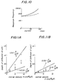
- Fig. 10 shows the relationship of the response frequency to the current flowing in the semiconductor light-emitting device. Since all the injected carriers are confined within the In 1-X Ga X As 1-Y P Y active layers 3 and 4 in the present device, the response frequency is much higher in the semiconductor light-emitting device according to the present invention (shown by the solid line) than in the conventional device (shown by the broken line) as shown in Fig. 10.
- the substrate and the layers thereon may take other values of thicknesses and carrier densities than those defined hereinabove with respect to the preferred embodi.ment.
- the carrier density of the n-InP substrate 1 may be 1 x 10 18 - 5 x 10 18 cm - 3 in which bulk resistance is low
- the carrier density of the n-InP clad layer 2 may be 1 x 10 18 - 5 x 10 18 cm- 3
- the dopant of said two layers may be Sn or S as well as Te.
- the thickness of the n-InP clad layer 2 may be 2 - 20 ⁇ m which is easily controllable during growth of the crystal.
- the quantity of dopant of the p-In 1-X Ga X As 1-Y P Y active layer 4 is easy to control when the carrier density is made 1 x 10 18 cm- 3 or higher for high speed response, the control becomes difficult at a carrier density of 1 x 10 19 cm- 3 or higher because the depth of diffusion becomes too large. Also,at a.carrier density of 1 x 10 19 cm- 3 or higher, the crystal is distorted and light-emitting efficiency is reduced. Therefore, the preferred carrier density of the p-In 1-X Ga X As 1-Y P Y active layer 4 is 1 x 10 18 - 1 x 1 0 19 cm -3.
- the thickness of the p-In 1-X Ga X As 1-Y P Y active layer 4 may be 0.1 ⁇ m or larger for easy control of the thickness of the epitaxial layer, the thickness is preferably 0.1 - 2 ⁇ m because the thickness of the layer is required to be equal to or smaller than the diffusion length of the minority carrier (normally of the order of 2 ⁇ m).
- the depth of diffusion of Zn which is a p-type dopant, shown in Fig. 11A, is several times larger than the depth of diffusion of any of other p-type dopants, such as Cd, Mg and Be, shown in Fig. 11B.
- the optimum range of the thickness is, as seen from Fig. 11B, from 0.1 x ⁇ m to 0.5 x ⁇ m, provided that the carrier density is defined as the number of carriers per cm 3 .
- the carrier density of the undoped In 1-X Ga X As 1-Y P Y active layer 3 is preferably 1 x 10 17 cm- 3 or lower,which is easily achievable and in which yield rate is high during growth of crystal.
Landscapes
- Led Devices (AREA)
- Semiconductor Lasers (AREA)
Abstract
Description
- This invention relates to a semiconductor light-emitting device.
- In a prior art high-speed responding light-emitting diode of double-hetero structure type of In1-XGaXAs1-YPY/InP, it was conventional practice to dope a p-In1-XGaXAs1-YPY active layer with Zn, which is a p-type impurity, at a high density of 3-10x1018cm-3 and to make this active layer grow epitaxially on an n-type InP clad layer to thereby increase the response speed (see, for example, Electronics Letters, 1983, Vol.19 No. 23, pp 963-965 and The Preprints 6P-H-8 for 30th Lectures of Federation of Applied Physcis Societies, Spring 1983).
- Referring to Fig. 1 of the drawings of the present application, an n-InP substrate 1 is doped with Te at a density of 1 x 1018cm-3; a p-InP clad layer is doped with Zn at a density of 3 x 10 cm and a p-In1-WGaWAs1-ZPZ contact layer 6 is doped with Zn at a density of 3 x 10 cm .
- Fig. 2 shows the carrier density profile of the layers of the light-emitting diode having the structure shown in Fig. 1. In Fig. 2,
numerals reference numerals active layer 4 is doped with Zn, a p-type impurity, at a high density, Zn is diffused into the n-InP clad layer 2 during the epitaxial growth as shown by the broken line in Fig. 2, to make a portion of the n-InP clade layer 2 p-InP. For this reason, a remote junction is produced in which the p-n junction is shifted from the interface between the p-In1-XGaXAs1-YPYactive layer 4 and the n-InP clad layer 2 into the n-InP clad layer 2. - Fig. 3 shows the energy band profile of the layers of Fig. 2. In Fig. 3,
reference numerals reference numerals InP clad layer 2 as shown in Fig. 3, a portion of the carriers flow out from the p-In1-XGaXAs1-YPYactive layer 4, which is the light-emitting region, into the n-InP clad layer, to thereby reduce the light-emitting output. - Furthermore, since the remote junction makes the carrier enclosure incomplete, reduction in the response speed is inevitable, even when the p-type impurity Zn is doped at a high density.
- To avoid the remote junction, it is conventional to provide sequentially the n-
InP layer 2 on the n-InP substrate 1, the undoped In1-XGaXAs1-YPYactive layer 3 on the n-InP layer 2, a p-InP clad layer 5' doped with Zn at a high density on theactive layer 3, and the p-In1-WGaWAs1-ZPZ contact layer 6 on the p-InP clad layer 5'. - Fig. 4 shows the carrier density profile of a light-emitting diode having the sequentially provided layers as described above. As shown by a broken line in Fig. 4, a p-n junction is formed in the
active layer 3 by diffusing Zn from the p-InP clad layer 5' into the In1-XGaXAs1-YPYactive layer 3 during the growth of the crystal. In the light-emitting device produced by the method described above, however, a half-value width of the light-emitting spectrum is enlarged, as shown in the curve (b) of Fig. 5. This is because, in the above-described method, Zn is diffused substantially over the entire region of the In1-XGaXAs1-YPYactive layer 3 which distorts the crystal of the In1-XGaXAs1-YPY active layer, or, even in the case where Zn is not diffused over the entire region, the p-n junction is formed in about the middle of the In1-XGaXAs1-YPYactive layer 3. - The light-emitting device produced by the method described above is, in spite of its high response speed, not suitable for high speed data transmission through optical fibres, because of the large half-value width of its light-emitting spectrum. That is, the data transmittable distance through optical fibres depends upon the half-value width of the light-emitting spectrum of the light-emitting device as shown in Figure 6. In the case where the half-value width is 160 nm, as shown by the curve (b) in Fig. 5, data transmission over a distance of 0.8 km or larger is practically impossible, as shown by a broken line in Fig. 6. The conventional light-emitting device produced by Zn diffusion as described above has a further disadvantage that uneven Zn diffusion in the In1-XGaXAs1-YPY
active layer 3 in the production process causes variation in the characteristics of the device. - Accordingly, an object of the present invention is to provide a semiconductor light-emitting device having an increased response speed and an intensified light-emitting output.
- Another object of the present invention is to provide a semiconductor light-emitting device having a narrowed half value width of the light-emitting spectrum.
- In accordance with the invention there is provided a semiconductor light-emitting device comprising an n-InP clad layer, an undoped In1-XGaXAs1-YPY active layer formed on the n-InP clad layer, and a p-In1-XGaXAs1-YPY active layer formed on the In1-XGaXAs1-YPY active layer, characterised by a p-n junction formed on the interface between the n-InP layer and the In1-XGaXAs1-YPY active layer or in the neighbourhood thereof.
- The structure of the present invention overcomes the difficulty of the conventional light-emitting device, i.e. the remote junction, in which the p-n junction position is formed within the n-InP clad layer. Accordingly, the light-emitting device according to the present invention has important characteristics such as high response speed and light-emitting output and a small half value width of light-emitting spectrum, and can be used as a semiconductor light-emitting device suitable for high speed data transmission through optical fibres.
- Furthermore, since the p-n junction position is formed easily on the interface, or in its neighbourhood, between the n-InP clad layer and the undoped In1-XGaXAs1-YPY active layer, control is easily performed during growth of the crystal, and the yield rate and the reliability of the device can be greatly increased.
- The invention will be better understood from the following description taken in connection with the accompanying drawings in which:
- Fig. 1 is a sectional view showing the structure of a conventional semiconductor light-emitting device;
- Fig. 2 is an illustration of the carrier density profile of the layers of the device shown in Fig. 1 and the junction position thereof;
- Fig. 3 is an illustration of the band profile of the layers of the device shown in Fig. 1;
- Fig. 4 is an illustration of the carrier density profile of the layers of another conventional semiconductor light-emitting device and the junction position thereof;
- Fig. 5 is a characteristics diagram of the light-emitting spectrum;
- Fig. 6 is a graph showing the relationship between the transmittable distance and the half value width of the light-emitting spectrum during high speed modulation;
- Fig. 7 is a sectional view showing the structure of an embodiment of the present invention;
- Fig. 8 is an illustration of the carrier density profile of the layers of the device shown in Fig. 7 and the junction position thereof;
- Fig. 9 is a current-light-emitting output characteristics diagram of the semiconductor light-emitting device;
- Fig. 10 is a current-response frequency characteristics diagram of the semiconductor light-emitting device;
- Fig. 11A is a graph showing the relationship between the depth of diffusion of a dopant within the undoped In1-XGaXAs1-YPY active layer during growth of crystal and the carrier density in the case where Zn is used as the p-type dopant; and
- Fig. 11B is a graph showing the depth of diffusion of a dopant within the undoped In1-XGaXAs1-YPY active layer during growth of crystal and the carrier density in the case where any of Cd, Mg and Be is used as the p-type dopant.
- With reference now to the drawings, a preferred embodiment of the present invention will be described in detail. Fig. 7 shows a structure of a semiconductor light-emitting device according to the present invention, in which reference numeral 1 denotes an n-InP substrate doped with Te in the density of 1 x 1018 cm-3. On the n-InP substrate 1, there is formed an n-
InP clad layer 2 doped with Te at a density of 1 x 1018 cm-3, in the thickness of 5 µm, by epitaxial growth. On the n-InP clad layer 2, there is formed an undoped In1-XGaXAs1-YPYactive layer 3 in the thickness of 0.5 µm by epitaxial growth. On the In1-XGaXAs1-YPYactive layer 3, there is formed a p-In1-XGaXAs1-YPYactive layer 4 doped with Zn at a density of 5 x 1018 cm-3, in the thickness of 1 µm,by epitaxial growth. On the p-Inl-X GaXAs1-YPYactive layer 4, there is formed a p-InP clad layer 5 doped with Zn at a density of 3 x 1018 cm-3, in the thickness of 1 µm, by epitaxial growth. On the p-InPclad layer 5, there is formed a p-In1-WGaWAs1-ZPZ contact layer 6 doped with Zn at a density of 3 x 1018 cm-3, in the thickness of 1 µm, by epitaxial growth. In this manner, theselayers - As described above, when the undoped In1-XGaXAs1-YPY
active layer 3 is epitaxially grown in the thickness of 0.5 µm and, thereafter, the Zn-doped p-In1-XGaXAs1-YPYactive layer 4 and p-InP clad layer 5 are sequentially epitaxially grown, Zn in the Zn-doped p-In1-XGaXAs1-YPYactive layer 4 is diffused in the thickness of 0.5 µm into the undoped In1-XGaXAs1-YPYactive layer 3. - Fig. 8 shows the carrier density profile of the layers of the semiconductor light-emitting device of Fig. 7, in which Zn of the p-In1-XGaXAs1-YPY
active layer 4 is diffused as shown by the broken line and a p-n junction is formed in the neighborhood of the interface between the In1-XGaXAs1-YPYactive layer 3 and the n-InP clad layer 2. By the p-n junction formed in this manner, the injected carriers are confined completely within the In1-XGaXAs1-YPYactive layer clad layer 2. For this reason, all the carriers contribute to emission of light. In fact, as shown in Fig. 9, the semiconductor light-emitting device according to the present invention provides a markedly larger light-emitting output shown by the solid line than that provided by the conventional semiconductor light-emitting device (shown by the broken line). Fig. 10 shows the relationship of the response frequency to the current flowing in the semiconductor light-emitting device. Since all the injected carriers are confined within the In1-XGaXAs1-YPYactive layers - In the present invention, the substrate and the layers thereon may take other values of thicknesses and carrier densities than those defined hereinabove with respect to the preferred embodi.ment. For example, the carrier density of the n-InP substrate 1 may be 1 x 10¹⁸ - 5 x 1018 cm-3 in which bulk resistance is low, the carrier density of the n-
InP clad layer 2 may be 1 x 10¹⁸ - 5 x 1018 cm-3, and the dopant of said two layers may be Sn or S as well as Te. Further, the thickness of the n-InP clad layer 2 may be 2 - 20 µm which is easily controllable during growth of the crystal. - While the quantity of dopant of the p-In1-XGaXAs1-YPY
active layer 4 is easy to control when the carrier density is made 1 x 1018 cm-3 or higher for high speed response, the control becomes difficult at a carrier density of 1 x 1019 cm-3 or higher because the depth of diffusion becomes too large. Also,at a.carrier density of 1 x 10 19 cm-3 or higher, the crystal is distorted and light-emitting efficiency is reduced. Therefore, the preferred carrier density of the p-In1-XGaXAs1-YPYactive layer 4 is 1 x 10¹⁸ - 1 x 1019 cm-3. While the thickness of the p-In1-XGaXAs1-YPYactive layer 4 may be 0.1 µm or larger for easy control of the thickness of the epitaxial layer, the thickness is preferably 0.1 - 2 µm because the thickness of the layer is required to be equal to or smaller than the diffusion length of the minority carrier (normally of the order of 2 µm). The p-Inl-X GaXAs1-YPY active layer is lattice-matched with the n-InP cladlayer 2 and its band gap energy is in the range from 0.75 eV (for example, X=0.42, Y=0.10) to 1.2 eV (for example, X=0.09, Y=0.80) which is the low loss region of quartz fibre. The p-type dopant of the p-In1-XGaXAs1-YPYactive layer 4 may be any of Cd, Mg and Be as well as Zn. During growth of crystal, the p-type dopant is diffused into the undoped In1-XGaXAs1-YPYactive layer 3 and the depth of its diffusion is substantially proportional to the density of the p-type dopant and is dependent upon the kind of the dopant. Figs. 11A and 11B show the relationship between the depth of diffusion of a dopant into the undoped In1-XGaXAs1-YPY active layer during growth of crystal and the carrier density. The depth of diffusion of Zn, which is a p-type dopant, shown in Fig. 11A, is several times larger than the depth of diffusion of any of other p-type dopants, such as Cd, Mg and Be, shown in Fig. 11B. - Accordingly, the optimum value of the thickness of the undoped In1-XGaXAs1-YPY
active layer 3 is dependent upon the kind and density of the p-type dopant of the p-Inl-XGaX As1-YPYactive layer 4. Accordingly, assuming that the dopant of the p-In1-XGaXAs1-YPYactive layer 4 is Zn and the carrier density of theactive layer 4 is P, the optimum range of the thickness of the undoped In1-XGaXAs1-YPYactive layer 3 is, as seen from Fig. 11A, from 0.3 x


active layer 3 is preferably 1 x 1017 cm-3 or lower,which is easily achievable and in which yield rate is high during growth of crystal. Further, the undoped In1-XGaXAs1-YPYactive layer 3 is lattice-matched with the n-InP cladlayer 2 and its band gap energy is selected in the range from 0.75 eV (for example, X=0.42, Y=0.10) to 1.2 eV (for example, X=0.09, Y=0.80) which is the low loss region of quartz fibre . - The carrier density of the p-InP clad
layer 5 is taken to be substantially equal to the carrier density of the p-In1-XGaXAs1-YPYactive layer 4, that is, in the range 1 x 10¹⁸ - 1 x 1019 cm-3, and the thickness of the p-InP cladlayer 5 is taken in the range 0.2 - 2.0 µm so as to efficiently confine the injected carriers within the undoped In1-XGaXAs1-YPYactive layer 3 and the p-Inl-XGaX Asl-yPyactive layer 4. The carrier density of the p-Inl-W GaWAs1-ZPZ contact layer 6 is taken in the range 1 x 10¹⁸ - 1 x 1019 cm-3 so as to reduce the contact resistance with the p-side electrode metal. The thickness of the p-Inl-W GaWAs1-ZPZ contact layer 6 is preferably in the range 0.1 - 1.0 µm. - In the foregoing description of the embodiment, while the undoped In1-XGaXAs1-YPY
active layer 3 and p-In1-XGaX As1-YPYactive layer 4 have been described, the material of the device according to the present invention is not limited thereto but other materials such as In1-XGaXAs1-YSbY/InSb (band gap from 0.35 eV to 0.70 eV) and Ga1-XAlXAs1-YSbY/GaSb (band gap from 0.70 eV to 1.60 eV) may be likewise utilized by liquid phase epitaxial growth or molecular beam epitaxial growth.
Claims (4)

Applications Claiming Priority (2)
| Application Number | Priority Date | Filing Date | Title |
|---|---|---|---|
| JP195529/83 | 1983-10-19 | ||
| JP58195529A JPS6086879A (en) | 1983-10-19 | 1983-10-19 | Manufacturing method of semiconductor light emitting device |
Publications (3)
| Publication Number | Publication Date |
|---|---|
| EP0140645A2 true EP0140645A2 (en) | 1985-05-08 |
| EP0140645A3 EP0140645A3 (en) | 1987-09-16 |
| EP0140645B1 EP0140645B1 (en) | 1993-07-28 |
Family
ID=16342600
Family Applications (1)
| Application Number | Title | Priority Date | Filing Date |
|---|---|---|---|
| EP84307115A Expired - Lifetime EP0140645B1 (en) | 1983-10-19 | 1984-10-17 | Semiconductor light-emitting device |
Country Status (4)
| Country | Link |
|---|---|
| US (1) | US4623907A (en) |
| EP (1) | EP0140645B1 (en) |
| JP (1) | JPS6086879A (en) |
| DE (1) | DE3486185T2 (en) |
Cited By (2)
| Publication number | Priority date | Publication date | Assignee | Title |
|---|---|---|---|---|
| EP0260110A3 (en) * | 1986-09-12 | 1989-04-05 | Nec Corporation | A double heterostructure light emitting diode |
| EP0704914A1 (en) * | 1994-09-28 | 1996-04-03 | Shin-Etsu Handotai Company Limited | Light emitting device |
Families Citing this family (3)
| Publication number | Priority date | Publication date | Assignee | Title |
|---|---|---|---|---|
| US4680607A (en) * | 1984-05-11 | 1987-07-14 | Sanyo Electric Co., Ltd. | Photovoltaic cell |
| JP4023893B2 (en) * | 1997-06-06 | 2007-12-19 | 沖電気工業株式会社 | Light emitting element array and light emitting element |
| CN1314088C (en) * | 2003-11-10 | 2007-05-02 | 四川大学 | Double pole transistor structure design of low start voltage gallium arsenide base new structure hetero junction |
Family Cites Families (4)
| Publication number | Priority date | Publication date | Assignee | Title |
|---|---|---|---|---|
| US4132960A (en) | 1977-03-28 | 1979-01-02 | Xerox Corporation | Single longitudinal mode gaas/gaalas double heterostructure laser |
| US4313125A (en) * | 1979-06-21 | 1982-01-26 | Bell Telephone Laboratories, Incorporated | Light emitting semiconductor devices |
| JPS5627987A (en) * | 1979-08-15 | 1981-03-18 | Kokusai Denshin Denwa Co Ltd <Kdd> | Semiconductor laser |
| JPS56107588A (en) * | 1980-01-30 | 1981-08-26 | Fujitsu Ltd | Semiconductor light emitting element |
-
1983
- 1983-10-19 JP JP58195529A patent/JPS6086879A/en active Granted
-
1984
- 1984-10-17 DE DE84307115T patent/DE3486185T2/en not_active Expired - Fee Related
- 1984-10-17 EP EP84307115A patent/EP0140645B1/en not_active Expired - Lifetime
- 1984-10-18 US US06/662,043 patent/US4623907A/en not_active Expired - Lifetime
Cited By (3)
| Publication number | Priority date | Publication date | Assignee | Title |
|---|---|---|---|---|
| EP0260110A3 (en) * | 1986-09-12 | 1989-04-05 | Nec Corporation | A double heterostructure light emitting diode |
| EP0704914A1 (en) * | 1994-09-28 | 1996-04-03 | Shin-Etsu Handotai Company Limited | Light emitting device |
| US5808324A (en) * | 1994-09-28 | 1998-09-15 | Shin-Etsu Handotai Co., Ltd | Light emitting device |
Also Published As
| Publication number | Publication date |
|---|---|
| DE3486185T2 (en) | 1993-11-04 |
| JPS6086879A (en) | 1985-05-16 |
| US4623907A (en) | 1986-11-18 |
| EP0140645B1 (en) | 1993-07-28 |
| JPH0325032B2 (en) | 1991-04-04 |
| DE3486185D1 (en) | 1993-09-02 |
| EP0140645A3 (en) | 1987-09-16 |
Similar Documents
| Publication | Publication Date | Title |
|---|---|---|
| EP0132081B1 (en) | Semiconductor laser device | |
| EP0457571A2 (en) | Strained superlattice semiconductor structure | |
| EP0163546B1 (en) | Process for fabricating an avalanche photodiode and an avalanche photodiode thus-obtained | |
| US4794606A (en) | Opto-electronic device | |
| CA1128634A (en) | Semiconductor laser structure and manufacture | |
| EP0181448A2 (en) | Method of manufacturing a compound semiconductor light-emitting diode | |
| US5432361A (en) | Low noise avalanche photodiode having an avalanche multiplication layer of InAlAs/InGaAlAs | |
| US5847415A (en) | Light emitting device having current blocking structure | |
| US4184170A (en) | Light emitting diode | |
| EP0314372A2 (en) | Current confinement and blocking region for semiconductor devices | |
| GB2082381A (en) | Semiconductor laser | |
| Razeghi et al. | cw operation of 1.57‐μm Ga x In1− x As y P1− y InP distributed feedback lasers grown by low‐pressure metalorganic chemical vapor deposition | |
| EP0140645A2 (en) | Semiconductor light-emitting device | |
| EP0500351A2 (en) | Semiconductor laser | |
| EP0293000B1 (en) | Light emitting device | |
| US5270246A (en) | Manufacturing method of semiconductor multi-layer film and semiconductor laser | |
| US4706253A (en) | High speed InGaAsP lasers by gain enhancement doping | |
| US5346837A (en) | Method of making avalanche photodiode | |
| CA1234421A (en) | Semiconductor light-emitting device | |
| US6507043B1 (en) | Epitaxially-grown backward diode | |
| JP2962069B2 (en) | Waveguide structure semiconductor photodetector | |
| JPS6244717B2 (en) | ||
| JPH0712103B2 (en) | Semiconductor laser device | |
| JPS61228684A (en) | semiconductor light emitting device | |
| JPH03297173A (en) | Semiconductor optical detector device |
Legal Events
| Date | Code | Title | Description |
|---|---|---|---|
| PUAI | Public reference made under article 153(3) epc to a published international application that has entered the european phase |
Free format text: ORIGINAL CODE: 0009012 |
|
| AK | Designated contracting states |
Designated state(s): DE FR GB SE |
|
| PUAL | Search report despatched |
Free format text: ORIGINAL CODE: 0009013 |
|
| AK | Designated contracting states |
Kind code of ref document: A3 Designated state(s): DE FR GB SE |
|
| 17P | Request for examination filed |
Effective date: 19880310 |
|
| 17Q | First examination report despatched |
Effective date: 19901015 |
|
| GRAA | (expected) grant |
Free format text: ORIGINAL CODE: 0009210 |
|
| AK | Designated contracting states |
Kind code of ref document: B1 Designated state(s): DE FR GB SE |
|
| REF | Corresponds to: |
Ref document number: 3486185 Country of ref document: DE Date of ref document: 19930902 |
|
| ET | Fr: translation filed | ||
| PLBE | No opposition filed within time limit |
Free format text: ORIGINAL CODE: 0009261 |
|
| STAA | Information on the status of an ep patent application or granted ep patent |
Free format text: STATUS: NO OPPOSITION FILED WITHIN TIME LIMIT |
|
| 26N | No opposition filed | ||
| EAL | Se: european patent in force in sweden |
Ref document number: 84307115.0 |
|
| PGFP | Annual fee paid to national office [announced via postgrant information from national office to epo] |
Ref country code: SE Payment date: 20011005 Year of fee payment: 18 |
|
| PGFP | Annual fee paid to national office [announced via postgrant information from national office to epo] |
Ref country code: FR Payment date: 20011010 Year of fee payment: 18 |
|
| PGFP | Annual fee paid to national office [announced via postgrant information from national office to epo] |
Ref country code: GB Payment date: 20011017 Year of fee payment: 18 |
|
| PGFP | Annual fee paid to national office [announced via postgrant information from national office to epo] |
Ref country code: DE Payment date: 20011029 Year of fee payment: 18 |
|
| REG | Reference to a national code |
Ref country code: GB Ref legal event code: IF02 |
|
| PG25 | Lapsed in a contracting state [announced via postgrant information from national office to epo] |
Ref country code: GB Free format text: LAPSE BECAUSE OF NON-PAYMENT OF DUE FEES Effective date: 20021017 |
|
| PG25 | Lapsed in a contracting state [announced via postgrant information from national office to epo] |
Ref country code: SE Free format text: LAPSE BECAUSE OF NON-PAYMENT OF DUE FEES Effective date: 20021018 |
|
| PG25 | Lapsed in a contracting state [announced via postgrant information from national office to epo] |
Ref country code: DE Free format text: LAPSE BECAUSE OF NON-PAYMENT OF DUE FEES Effective date: 20030501 |
|
| EUG | Se: european patent has lapsed | ||
| GBPC | Gb: european patent ceased through non-payment of renewal fee |
Effective date: 20021017 |
|
| PG25 | Lapsed in a contracting state [announced via postgrant information from national office to epo] |
Ref country code: FR Free format text: LAPSE BECAUSE OF NON-PAYMENT OF DUE FEES Effective date: 20030630 |
|
| REG | Reference to a national code |
Ref country code: FR Ref legal event code: ST |