EP0140645A2 - Lichtemittierende Halbleitervorrichtung - Google Patents
Lichtemittierende Halbleitervorrichtung Download PDFInfo
- Publication number
- EP0140645A2 EP0140645A2 EP84307115A EP84307115A EP0140645A2 EP 0140645 A2 EP0140645 A2 EP 0140645A2 EP 84307115 A EP84307115 A EP 84307115A EP 84307115 A EP84307115 A EP 84307115A EP 0140645 A2 EP0140645 A2 EP 0140645A2
- Authority
- EP
- European Patent Office
- Prior art keywords
- active layer
- layer
- emitting device
- undoped
- light
- Prior art date
- Legal status (The legal status is an assumption and is not a legal conclusion. Google has not performed a legal analysis and makes no representation as to the accuracy of the status listed.)
- Granted
Links
- 239000004065 semiconductor Substances 0.000 title claims abstract description 22
- 239000002019 doping agent Substances 0.000 claims description 18
- 229910052793 cadmium Inorganic materials 0.000 claims description 5
- 238000001228 spectrum Methods 0.000 abstract description 9
- 239000013078 crystal Substances 0.000 description 10
- 238000009792 diffusion process Methods 0.000 description 10
- 239000000969 carrier Substances 0.000 description 6
- 239000000758 substrate Substances 0.000 description 6
- 230000005540 biological transmission Effects 0.000 description 3
- 238000010586 diagram Methods 0.000 description 3
- 239000012535 impurity Substances 0.000 description 3
- 238000000034 method Methods 0.000 description 3
- 230000003287 optical effect Effects 0.000 description 3
- 230000001419 dependent effect Effects 0.000 description 2
- 239000000835 fiber Substances 0.000 description 2
- 239000000463 material Substances 0.000 description 2
- 239000010453 quartz Substances 0.000 description 2
- VYPSYNLAJGMNEJ-UHFFFAOYSA-N silicon dioxide Inorganic materials O=[Si]=O VYPSYNLAJGMNEJ-UHFFFAOYSA-N 0.000 description 2
- 229910005542 GaSb Inorganic materials 0.000 description 1
- -1 at a high density Substances 0.000 description 1
- WPYVAWXEWQSOGY-UHFFFAOYSA-N indium antimonide Chemical compound [Sb]#[In] WPYVAWXEWQSOGY-UHFFFAOYSA-N 0.000 description 1
- 239000007791 liquid phase Substances 0.000 description 1
- 238000004519 manufacturing process Methods 0.000 description 1
- 239000002184 metal Substances 0.000 description 1
- 229910052751 metal Inorganic materials 0.000 description 1
- 229910052718 tin Inorganic materials 0.000 description 1
Images


Classifications
-
- H—ELECTRICITY
- H10—SEMICONDUCTOR DEVICES; ELECTRIC SOLID-STATE DEVICES NOT OTHERWISE PROVIDED FOR
- H10H—INORGANIC LIGHT-EMITTING SEMICONDUCTOR DEVICES HAVING POTENTIAL BARRIERS
- H10H20/00—Individual inorganic light-emitting semiconductor devices having potential barriers, e.g. light-emitting diodes [LED]
- H10H20/80—Constructional details
- H10H20/81—Bodies
- H10H20/8215—Bodies characterised by crystalline imperfections, e.g. dislocations; characterised by the distribution of dopants, e.g. delta-doping
-
- H—ELECTRICITY
- H10—SEMICONDUCTOR DEVICES; ELECTRIC SOLID-STATE DEVICES NOT OTHERWISE PROVIDED FOR
- H10H—INORGANIC LIGHT-EMITTING SEMICONDUCTOR DEVICES HAVING POTENTIAL BARRIERS
- H10H20/00—Individual inorganic light-emitting semiconductor devices having potential barriers, e.g. light-emitting diodes [LED]
- H10H20/80—Constructional details
- H10H20/81—Bodies
- H10H20/811—Bodies having quantum effect structures or superlattices, e.g. tunnel junctions
-
- H—ELECTRICITY
- H10—SEMICONDUCTOR DEVICES; ELECTRIC SOLID-STATE DEVICES NOT OTHERWISE PROVIDED FOR
- H10H—INORGANIC LIGHT-EMITTING SEMICONDUCTOR DEVICES HAVING POTENTIAL BARRIERS
- H10H20/00—Individual inorganic light-emitting semiconductor devices having potential barriers, e.g. light-emitting diodes [LED]
- H10H20/80—Constructional details
- H10H20/81—Bodies
- H10H20/822—Materials of the light-emitting regions
- H10H20/824—Materials of the light-emitting regions comprising only Group III-V materials, e.g. GaP
Definitions
- This invention relates to a semiconductor light-emitting device.
- an n-InP substrate 1 is doped with Te at a density of 1 x 10 18 cm -3 ; a p-InP clad layer is doped with Zn at a density of 3 x 10 cm and a p-In 1-W Ga W As 1-Z P Z contact layer 6 is doped with Zn at a density of 3 x 10 cm .
- Fig. 2 shows the carrier density profile of the layers of the light-emitting diode having the structure shown in Fig. 1.
- numerals 1,2,4,5 and 6 along the horizontal axis correspond to the reference numerals 1,2,4, 5 and 6 denoting the layers of the structure of Fig. 1.
- the p-In 1-X Ga X As 1-Y P Y active layer 4 is doped with Zn, a p-type impurity, at a high density, Zn is diffused into the n-InP clad layer 2 during the epitaxial growth as shown by the broken line in Fig. 2, to make a portion of the n-InP clade layer 2 p-InP.
- Fig. 3 shows the energy band profile of the layers of Fig. 2.
- reference numerals 1,2,4,5 and 6 along the horizontal axis correspond to the reference numerals 1,2,4,5 and 6, respectively, denoting the layers in Figs. 1 and 2.
- a portion of the carriers flow out from the p-In 1-X Ga X As 1-Y P Y active layer 4, which is the light-emitting region, into the n-InP clad layer, to thereby reduce the light-emitting output.
- the remote junction makes the carrier enclosure incomplete, reduction in the response speed is inevitable, even when the p-type impurity Zn is doped at a high density.
- the n-InP layer 2 on the n-InP substrate 1 the undoped In 1-X Ga X As 1-Y P Y active layer 3 on the n-InP layer 2, a p-InP clad layer 5' doped with Zn at a high density on the active layer 3, and the p-In 1-W Ga W As 1-Z P Z contact layer 6 on the p-InP clad layer 5'.
- Fig. 4 shows the carrier density profile of a light-emitting diode having the sequentially provided layers as described above.
- a p-n junction is formed in the active layer 3 by diffusing Zn from the p-InP clad layer 5' into the In 1-X Ga X As 1-Y P Y active layer 3 during the growth of the crystal.
- a half-value width of the light-emitting spectrum is enlarged, as shown in the curve (b) of Fig. 5.
- an object of the present invention is to provide a semiconductor light-emitting device having an increased response speed and an intensified light-emitting output.
- Another object of the present invention is to provide a semiconductor light-emitting device having a narrowed half value width of the light-emitting spectrum.
- a semiconductor light-emitting device comprising an n-InP clad layer, an undoped In 1-X Ga X As 1-Y P Y active layer formed on the n-InP clad layer, and a p-In 1-X Ga X As 1-Y P Y active layer formed on the In 1-X Ga X As 1-Y P Y active layer, characterised by a p-n junction formed on the interface between the n-InP layer and the In 1-X Ga X As 1-Y P Y active layer or in the neighbourhood thereof.
- the p-n junction position is formed easily on the interface, or in its neighbourhood, between the n-InP clad layer and the undoped In 1-X Ga X As 1-Y P Y active layer, control is easily performed during growth of the crystal, and the yield rate and the reliability of the device can be greatly increased.
- In 1-X Ga X As 1-Y P Y active layer 3 there is formed a p-In 1-X Ga X As 1-Y P Y active layer 4 doped with Zn at a density of 5 x 10 18 cm- 3 , in the thickness of 1 ⁇ m,by epitaxial growth.
- p-In l - X Ga X As 1-Y P Y active layer 4 there is formed a p-InP clad layer 5 doped with Zn at a density of 3 x 10 18 cm- 3 , in the thickness of 1 ⁇ m, by epitaxial growth.
- the undoped In 1-X Ga X As 1-Y P Y active layer 3 is epitaxially grown in the thickness of 0.5 ⁇ m and, thereafter, the Zn-doped p-In 1-X Ga X As 1-Y P Y active layer 4 and p-InP clad layer 5 are sequentially epitaxially grown, Zn in the Zn-doped p-In 1-X Ga X As 1-Y P Y active layer 4 is diffused in the thickness of 0.5 ⁇ m into the undoped In 1-X Ga X As 1-Y P Y active layer 3.
- Fig. 8 shows the carrier density profile of the layers of the semiconductor light-emitting device of Fig. 7, in which Zn of the p-In 1-X Ga X As 1-Y P Y active layer 4 is diffused as shown by the broken line and a p-n junction is formed in the neighborhood of the interface between the In 1-X Ga X As 1-Y P Y active layer 3 and the n-InP clad layer 2.
- the injected carriers are confined completely within the In 1-X Ga X As 1-Y P Y active layer 3 and 4 without flowing out into the n-InP clad layer 2. For this reason, all the carriers contribute to emission of light.
- Fig. 8 shows the carrier density profile of the layers of the semiconductor light-emitting device of Fig. 7, in which Zn of the p-In 1-X Ga X As 1-Y P Y active layer 4 is diffused as shown by the broken line and a p-n junction is formed in the neighborhood of the interface between the In 1-X Ga X As 1-Y P Y active layer
- the semiconductor light-emitting device according to the present invention provides a markedly larger light-emitting output shown by the solid line than that provided by the conventional semiconductor light-emitting device (shown by the broken line).
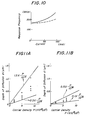
- Fig. 10 shows the relationship of the response frequency to the current flowing in the semiconductor light-emitting device. Since all the injected carriers are confined within the In 1-X Ga X As 1-Y P Y active layers 3 and 4 in the present device, the response frequency is much higher in the semiconductor light-emitting device according to the present invention (shown by the solid line) than in the conventional device (shown by the broken line) as shown in Fig. 10.
- the substrate and the layers thereon may take other values of thicknesses and carrier densities than those defined hereinabove with respect to the preferred embodi.ment.
- the carrier density of the n-InP substrate 1 may be 1 x 10 18 - 5 x 10 18 cm - 3 in which bulk resistance is low
- the carrier density of the n-InP clad layer 2 may be 1 x 10 18 - 5 x 10 18 cm- 3
- the dopant of said two layers may be Sn or S as well as Te.
- the thickness of the n-InP clad layer 2 may be 2 - 20 ⁇ m which is easily controllable during growth of the crystal.
- the quantity of dopant of the p-In 1-X Ga X As 1-Y P Y active layer 4 is easy to control when the carrier density is made 1 x 10 18 cm- 3 or higher for high speed response, the control becomes difficult at a carrier density of 1 x 10 19 cm- 3 or higher because the depth of diffusion becomes too large. Also,at a.carrier density of 1 x 10 19 cm- 3 or higher, the crystal is distorted and light-emitting efficiency is reduced. Therefore, the preferred carrier density of the p-In 1-X Ga X As 1-Y P Y active layer 4 is 1 x 10 18 - 1 x 1 0 19 cm -3.
- the thickness of the p-In 1-X Ga X As 1-Y P Y active layer 4 may be 0.1 ⁇ m or larger for easy control of the thickness of the epitaxial layer, the thickness is preferably 0.1 - 2 ⁇ m because the thickness of the layer is required to be equal to or smaller than the diffusion length of the minority carrier (normally of the order of 2 ⁇ m).
- the depth of diffusion of Zn which is a p-type dopant, shown in Fig. 11A, is several times larger than the depth of diffusion of any of other p-type dopants, such as Cd, Mg and Be, shown in Fig. 11B.
- the optimum range of the thickness is, as seen from Fig. 11B, from 0.1 x ⁇ m to 0.5 x ⁇ m, provided that the carrier density is defined as the number of carriers per cm 3 .
- the carrier density of the undoped In 1-X Ga X As 1-Y P Y active layer 3 is preferably 1 x 10 17 cm- 3 or lower,which is easily achievable and in which yield rate is high during growth of crystal.
Landscapes
- Led Devices (AREA)
- Semiconductor Lasers (AREA)
Applications Claiming Priority (2)
| Application Number | Priority Date | Filing Date | Title |
|---|---|---|---|
| JP195529/83 | 1983-10-19 | ||
| JP58195529A JPS6086879A (ja) | 1983-10-19 | 1983-10-19 | 半導体発光素子の製造方法 |
Publications (3)
| Publication Number | Publication Date |
|---|---|
| EP0140645A2 true EP0140645A2 (de) | 1985-05-08 |
| EP0140645A3 EP0140645A3 (en) | 1987-09-16 |
| EP0140645B1 EP0140645B1 (de) | 1993-07-28 |
Family
ID=16342600
Family Applications (1)
| Application Number | Title | Priority Date | Filing Date |
|---|---|---|---|
| EP84307115A Expired - Lifetime EP0140645B1 (de) | 1983-10-19 | 1984-10-17 | Lichtemittierende Halbleitervorrichtung |
Country Status (4)
| Country | Link |
|---|---|
| US (1) | US4623907A (de) |
| EP (1) | EP0140645B1 (de) |
| JP (1) | JPS6086879A (de) |
| DE (1) | DE3486185T2 (de) |
Cited By (2)
| Publication number | Priority date | Publication date | Assignee | Title |
|---|---|---|---|---|
| EP0260110A3 (en) * | 1986-09-12 | 1989-04-05 | Nec Corporation | A double heterostructure light emitting diode |
| EP0704914A1 (de) * | 1994-09-28 | 1996-04-03 | Shin-Etsu Handotai Company Limited | Lichtemittierende Vorrichtung |
Families Citing this family (3)
| Publication number | Priority date | Publication date | Assignee | Title |
|---|---|---|---|---|
| US4680607A (en) * | 1984-05-11 | 1987-07-14 | Sanyo Electric Co., Ltd. | Photovoltaic cell |
| JP4023893B2 (ja) * | 1997-06-06 | 2007-12-19 | 沖電気工業株式会社 | 発光素子アレイ及び発光素子 |
| CN1314088C (zh) * | 2003-11-10 | 2007-05-02 | 四川大学 | 一种低开启电压砷化镓基异质结双极晶体管 |
Family Cites Families (4)
| Publication number | Priority date | Publication date | Assignee | Title |
|---|---|---|---|---|
| US4132960A (en) | 1977-03-28 | 1979-01-02 | Xerox Corporation | Single longitudinal mode gaas/gaalas double heterostructure laser |
| US4313125A (en) * | 1979-06-21 | 1982-01-26 | Bell Telephone Laboratories, Incorporated | Light emitting semiconductor devices |
| JPS5627987A (en) * | 1979-08-15 | 1981-03-18 | Kokusai Denshin Denwa Co Ltd <Kdd> | Semiconductor laser |
| JPS56107588A (en) * | 1980-01-30 | 1981-08-26 | Fujitsu Ltd | Semiconductor light emitting element |
-
1983
- 1983-10-19 JP JP58195529A patent/JPS6086879A/ja active Granted
-
1984
- 1984-10-17 DE DE84307115T patent/DE3486185T2/de not_active Expired - Fee Related
- 1984-10-17 EP EP84307115A patent/EP0140645B1/de not_active Expired - Lifetime
- 1984-10-18 US US06/662,043 patent/US4623907A/en not_active Expired - Lifetime
Cited By (3)
| Publication number | Priority date | Publication date | Assignee | Title |
|---|---|---|---|---|
| EP0260110A3 (en) * | 1986-09-12 | 1989-04-05 | Nec Corporation | A double heterostructure light emitting diode |
| EP0704914A1 (de) * | 1994-09-28 | 1996-04-03 | Shin-Etsu Handotai Company Limited | Lichtemittierende Vorrichtung |
| US5808324A (en) * | 1994-09-28 | 1998-09-15 | Shin-Etsu Handotai Co., Ltd | Light emitting device |
Also Published As
| Publication number | Publication date |
|---|---|
| DE3486185T2 (de) | 1993-11-04 |
| JPS6086879A (ja) | 1985-05-16 |
| US4623907A (en) | 1986-11-18 |
| EP0140645B1 (de) | 1993-07-28 |
| JPH0325032B2 (de) | 1991-04-04 |
| DE3486185D1 (de) | 1993-09-02 |
| EP0140645A3 (en) | 1987-09-16 |
Similar Documents
| Publication | Publication Date | Title |
|---|---|---|
| EP0132081B1 (de) | Halbleiterlaser | |
| EP0457571A2 (de) | Halbleiterstruktur mit Übergitter unter Spannung | |
| EP0163546B1 (de) | Herstellungsverfahren einer Lawinenphotodiode und so hergestellte Lawinenphotodiode | |
| US4794606A (en) | Opto-electronic device | |
| CA1128634A (en) | Semiconductor laser structure and manufacture | |
| EP0181448A2 (de) | Verfahren zur Herstellung einer lichtemittierenden Diode aus einem Verbindungshalbleiter | |
| US5432361A (en) | Low noise avalanche photodiode having an avalanche multiplication layer of InAlAs/InGaAlAs | |
| US5847415A (en) | Light emitting device having current blocking structure | |
| US4184170A (en) | Light emitting diode | |
| EP0314372A2 (de) | Stromeingrenzungs- und Blockierungsgebiet für Halbleitervorrichtungen | |
| GB2082381A (en) | Semiconductor laser | |
| Razeghi et al. | cw operation of 1.57‐μm Ga x In1− x As y P1− y InP distributed feedback lasers grown by low‐pressure metalorganic chemical vapor deposition | |
| EP0140645A2 (de) | Lichtemittierende Halbleitervorrichtung | |
| EP0500351A2 (de) | Halbleiterlaser | |
| EP0293000B1 (de) | Lichtemittierende Vorrichtung | |
| US5270246A (en) | Manufacturing method of semiconductor multi-layer film and semiconductor laser | |
| US4706253A (en) | High speed InGaAsP lasers by gain enhancement doping | |
| US5346837A (en) | Method of making avalanche photodiode | |
| CA1234421A (en) | Semiconductor light-emitting device | |
| US6507043B1 (en) | Epitaxially-grown backward diode | |
| JP2962069B2 (ja) | 導波路構造半導体受光素子 | |
| JPS6244717B2 (de) | ||
| JPH0712103B2 (ja) | 半導体レ−ザ素子 | |
| JPS61228684A (ja) | 半導体発光素子 | |
| JPH03297173A (ja) | 半導体受光素子 |
Legal Events
| Date | Code | Title | Description |
|---|---|---|---|
| PUAI | Public reference made under article 153(3) epc to a published international application that has entered the european phase |
Free format text: ORIGINAL CODE: 0009012 |
|
| AK | Designated contracting states |
Designated state(s): DE FR GB SE |
|
| PUAL | Search report despatched |
Free format text: ORIGINAL CODE: 0009013 |
|
| AK | Designated contracting states |
Kind code of ref document: A3 Designated state(s): DE FR GB SE |
|
| 17P | Request for examination filed |
Effective date: 19880310 |
|
| 17Q | First examination report despatched |
Effective date: 19901015 |
|
| GRAA | (expected) grant |
Free format text: ORIGINAL CODE: 0009210 |
|
| AK | Designated contracting states |
Kind code of ref document: B1 Designated state(s): DE FR GB SE |
|
| REF | Corresponds to: |
Ref document number: 3486185 Country of ref document: DE Date of ref document: 19930902 |
|
| ET | Fr: translation filed | ||
| PLBE | No opposition filed within time limit |
Free format text: ORIGINAL CODE: 0009261 |
|
| STAA | Information on the status of an ep patent application or granted ep patent |
Free format text: STATUS: NO OPPOSITION FILED WITHIN TIME LIMIT |
|
| 26N | No opposition filed | ||
| EAL | Se: european patent in force in sweden |
Ref document number: 84307115.0 |
|
| PGFP | Annual fee paid to national office [announced via postgrant information from national office to epo] |
Ref country code: SE Payment date: 20011005 Year of fee payment: 18 |
|
| PGFP | Annual fee paid to national office [announced via postgrant information from national office to epo] |
Ref country code: FR Payment date: 20011010 Year of fee payment: 18 |
|
| PGFP | Annual fee paid to national office [announced via postgrant information from national office to epo] |
Ref country code: GB Payment date: 20011017 Year of fee payment: 18 |
|
| PGFP | Annual fee paid to national office [announced via postgrant information from national office to epo] |
Ref country code: DE Payment date: 20011029 Year of fee payment: 18 |
|
| REG | Reference to a national code |
Ref country code: GB Ref legal event code: IF02 |
|
| PG25 | Lapsed in a contracting state [announced via postgrant information from national office to epo] |
Ref country code: GB Free format text: LAPSE BECAUSE OF NON-PAYMENT OF DUE FEES Effective date: 20021017 |
|
| PG25 | Lapsed in a contracting state [announced via postgrant information from national office to epo] |
Ref country code: SE Free format text: LAPSE BECAUSE OF NON-PAYMENT OF DUE FEES Effective date: 20021018 |
|
| PG25 | Lapsed in a contracting state [announced via postgrant information from national office to epo] |
Ref country code: DE Free format text: LAPSE BECAUSE OF NON-PAYMENT OF DUE FEES Effective date: 20030501 |
|
| EUG | Se: european patent has lapsed | ||
| GBPC | Gb: european patent ceased through non-payment of renewal fee |
Effective date: 20021017 |
|
| PG25 | Lapsed in a contracting state [announced via postgrant information from national office to epo] |
Ref country code: FR Free format text: LAPSE BECAUSE OF NON-PAYMENT OF DUE FEES Effective date: 20030630 |
|
| REG | Reference to a national code |
Ref country code: FR Ref legal event code: ST |