EP0140975A1 - Appareil de gravure ionique reactive - Google Patents
Appareil de gravure ionique reactive Download PDFInfo
- Publication number
- EP0140975A1 EP0140975A1 EP84901223A EP84901223A EP0140975A1 EP 0140975 A1 EP0140975 A1 EP 0140975A1 EP 84901223 A EP84901223 A EP 84901223A EP 84901223 A EP84901223 A EP 84901223A EP 0140975 A1 EP0140975 A1 EP 0140975A1
- Authority
- EP
- European Patent Office
- Prior art keywords
- reactive ion
- ion etching
- substrate electrode
- vacuum container
- polytetrafluoroethylene
- Prior art date
- Legal status (The legal status is an assumption and is not a legal conclusion. Google has not performed a legal analysis and makes no representation as to the accuracy of the status listed.)
- Withdrawn
Links
Images

Classifications
-
- H—ELECTRICITY
- H01—ELECTRIC ELEMENTS
- H01J—ELECTRIC DISCHARGE TUBES OR DISCHARGE LAMPS
- H01J37/00—Discharge tubes with provision for introducing objects or material to be exposed to the discharge, e.g. for the purpose of examination or processing thereof
- H01J37/32—Gas-filled discharge tubes
- H01J37/32431—Constructional details of the reactor
- H01J37/32458—Vessel
- H01J37/32477—Vessel characterised by the means for protecting vessels or internal parts, e.g. coatings
-
- H—ELECTRICITY
- H01—ELECTRIC ELEMENTS
- H01J—ELECTRIC DISCHARGE TUBES OR DISCHARGE LAMPS
- H01J37/00—Discharge tubes with provision for introducing objects or material to be exposed to the discharge, e.g. for the purpose of examination or processing thereof
- H01J37/32—Gas-filled discharge tubes
- H01J37/32009—Arrangements for generation of plasma specially adapted for examination or treatment of objects, e.g. plasma sources
- H01J37/32082—Radio frequency generated discharge
-
- H—ELECTRICITY
- H01—ELECTRIC ELEMENTS
- H01J—ELECTRIC DISCHARGE TUBES OR DISCHARGE LAMPS
- H01J37/00—Discharge tubes with provision for introducing objects or material to be exposed to the discharge, e.g. for the purpose of examination or processing thereof
- H01J37/32—Gas-filled discharge tubes
- H01J37/32431—Constructional details of the reactor
- H01J37/32532—Electrodes
- H01J37/32559—Protection means, e.g. coatings
-
- H—ELECTRICITY
- H10—SEMICONDUCTOR DEVICES; ELECTRIC SOLID-STATE DEVICES NOT OTHERWISE PROVIDED FOR
- H10P—GENERIC PROCESSES OR APPARATUS FOR THE MANUFACTURE OR TREATMENT OF DEVICES COVERED BY CLASS H10
- H10P50/00—Etching of wafers, substrates or parts of devices
- H10P50/20—Dry etching; Plasma etching; Reactive-ion etching
- H10P50/24—Dry etching; Plasma etching; Reactive-ion etching of semiconductor materials
- H10P50/242—Dry etching; Plasma etching; Reactive-ion etching of semiconductor materials of Group IV materials
-
- H—ELECTRICITY
- H01—ELECTRIC ELEMENTS
- H01J—ELECTRIC DISCHARGE TUBES OR DISCHARGE LAMPS
- H01J2237/00—Discharge tubes exposing object to beam, e.g. for analysis treatment, etching, imaging
- H01J2237/32—Processing objects by plasma generation
- H01J2237/33—Processing objects by plasma generation characterised by the type of processing
- H01J2237/334—Etching
- H01J2237/3341—Reactive etching
Definitions
- This invention relates to a reactive ion etching apparatus in the manufacturing process for electronic parts, such as semiconductors.
- This invention is directed to provision of a reactive ion etching apparatus for Si series material, which increases an etching rate thereof without increasing the power from a power source.
- a conventional reactive ion etching apparatus for Si series material has a vacuum container 1 provided with an evacuation end connection 2 connected to an evacuation means (not shown), a working gas supply conduit 3, a substrate electrode 4, and an opposite electrode 5, the substrate electrode 4 connecting to a high frequency power source 6, the working gas having used a fluorine compound (CF 4 , C 3 F 8 , e t c. ) .
- Reference numeral 7 designates an object to be etched.
- Such reactive ion etching apparatus for 8i series material should increase the power from a power source in order to increase an etching rate of Si series material, whereby a selection ratio of etching rate to a resist material (etching rate of 8i series material/that of resist material) serving as the master pattern decreases, thereby having been defective in that the reactive ion etching as the master pattern cannot be carried out.
- a reactive ion etching apparatus of the invention is basically the same in construction as the conventional reactive ion etching apparatus for Si series material, in which the inner surface of a vacuum container, a substrate electrode, or an opposite electrode is coated with polytetrafluoroethylene, a ring made from polytetrafluoroethylene is provided around the object to be etched on the substrate electrode, or a perforated plate formed of polytetrafluoroethylene is interposed between the substrate electrode and the opposite electrode, so that when electric discharge starts in the working gas of fluorine compound (CF 4 , F 3 F 8 , etc.), not only a substance (ion or radical of fluorine and fluorine compound) contributing to etching is produced from the working gas, but also the substance contributing to the same is produced from the components: the ring and perforate plate, coated with polytetrafluoroethylene.
- the reactive ion etching apparatus of the invention has the particular effect such that the etching rate of Si series material increases without decreasing the selection ratio of
- Fig. 2 is a schematic view of the embodiment of a reactive ion etching apparatus for Si series material of the invention, in which reference numeral 8 designates a vacuum container, 9 designates an evacuation outlet, 10 designates a working gas supply inlet, 11 designates a substrate electrode, 12 designates an opposite electrode, 13 designates a high frequency power source, and 14 designates an object to be etched, 15 designates a perforated plate formed of polytetrafluoroethylene, the perforated plate 15 used in this embodiment having bores each of 8 mm in diameter, 10 mm in bore pitch, and 3 mm in thickness, 16 designates stays for supporting the perforated plate and formed of an alumina insulator, the stays 16 in this embodiment having been designed to keep an interval of 10 mm between the perforated bore plate and the object to be etched (the upper surface of wafer), and 17 designates a ring of polytetrafluoroethylene.
- reference numeral 8 designates a vacuum container
- 9 designates an evacuation outlet
- the ring 17 used in this embodiment is 101 mm in an inner diameter, 152 mm in an outer diameter, and 3 mm in thickness.
- the apparatus constructed as foregoing is used to carry out the reactive ion etching for Si series material of the invention under the following etching conditions:
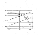
- Fig. 3 is a graph shoving the result in comparison of the selection ratio of the etching rate of 8i0 2 film to that of the resist material in this embodiment with the reactive ion etching carried out by use of the conventional apparatus in Fig. 1 under the same condition as this embodiment, in which the line A shows the result in this embodiment and B the conventional example.
- the ring of polytetrafluoroethylene is provided around the object to be etched and the perforated plate of polytetrafluoroethylene is provided between the opposite electrode and the substrate electrode, thereby enabling the etching rate of Si0 2 film to increase without reducing the selection ratio of etching rate to the resist material.
- the perforated plate 15 and ring 17 of polytetrafluoroethylene in this embodiment may be either one only.
- the ion etching apparatus of the invention of course has the effect as abovementioned.
- the object to be etched may alternatively be any one of single crystal, polycrystalline Si film and silicon nitride film.
- the Si series material reactive ion etching apparatus of the invention is so constructed that one, two or the whole of the inner surface of vacuum container, opposite electrode and substrate electrode, is coated with polytetrafluoroethylene, the ring formed thereof is provided around the object to be etched, or the perforated plate is interposed between the opposite electrode and the substrate electrode, thereby enabling the etching rate of Si series material to increase without reducing the selection ratio of etching rate to the resist, thereby having a higher etching effect.
Landscapes
- Physics & Mathematics (AREA)
- Engineering & Computer Science (AREA)
- Plasma & Fusion (AREA)
- Chemical & Material Sciences (AREA)
- Analytical Chemistry (AREA)
- Drying Of Semiconductors (AREA)
Abstract
L'appareil de gravure ionique réactive ci-décrit est fondamentalement analogue à un appareil conventionnel qui soumet un matériau à base de Fi à une gravure ionique réactive. Les surfaces internes d'un récipient sous vide (1) ou une électrode de substrat (4) et une électrode opposée (5) sont recouvertes de tétrafluorure de polyéthylène, et un anneau (17) en tétrafluorure de polyéthylène est disposé autour de l'objet à graver sur une électrode de substrat, ou bien une plaque poreuse (15) de tétrafluorure de polyéthylène est disposée entre l'électrode de substrat et l'électrode opposée. Par conséquent, lorsque la décharge commence à avoir lieu dans un gaz de traitement d'un composé de fluor (CF4, C3F8, etc.), des substances (ions ou radicaux de fluor et composés de fluor) qui contribuent à la gravure sont produites par le gaz de traitement, et des substances qui prennent part à la gravure sont également produites à partir des parties constituantes recouvertes de tétrafluorure de polyéthylène ainsi qu'à partir de l'anneau et de la plaque poreuse en tétrafluorure de polyéthylène. Il estainsi possible et avantageux, à la différence de l'art antérieur, d'accroître le taux de gravure d'un matériau à base de Si sans réduire le rapport de vitesse de gravure sélectionné en fonction de la réserve utilisée.
Applications Claiming Priority (4)
| Application Number | Priority Date | Filing Date | Title |
|---|---|---|---|
| JP46235/83 | 1983-03-18 | ||
| JP46236/83 | 1983-03-18 | ||
| JP58046235A JPS59172236A (ja) | 1983-03-18 | 1983-03-18 | 反応性イオンエツチング装置 |
| JP58046236A JPS59173273A (ja) | 1983-03-18 | 1983-03-18 | 反応性イオンエツチング装置 |
Publications (2)
| Publication Number | Publication Date |
|---|---|
| EP0140975A1 true EP0140975A1 (fr) | 1985-05-15 |
| EP0140975A4 EP0140975A4 (fr) | 1988-01-07 |
Family
ID=26386345
Family Applications (1)
| Application Number | Title | Priority Date | Filing Date |
|---|---|---|---|
| EP19840901223 Withdrawn EP0140975A4 (fr) | 1983-03-18 | 1984-03-19 | Appareil de gravure ionique reactive. |
Country Status (2)
| Country | Link |
|---|---|
| EP (1) | EP0140975A4 (fr) |
| WO (1) | WO1984003798A1 (fr) |
Cited By (9)
| Publication number | Priority date | Publication date | Assignee | Title |
|---|---|---|---|---|
| EP0323620A3 (en) * | 1987-12-25 | 1990-04-11 | Tokyo Electron Limited | Etching method and etching apparatus |
| WO1991017562A1 (fr) * | 1990-04-30 | 1991-11-14 | International Business Machines Corporation | Chambre de reaction plasmatique ayant des surfaces a revetement en diamant conducteur |
| EP0648861A1 (fr) * | 1993-10-15 | 1995-04-19 | Applied Materials, Inc. | Appareillage de traitement des semi-conducteurs |
| US5554854A (en) * | 1995-07-17 | 1996-09-10 | Eaton Corporation | In situ removal of contaminants from the interior surfaces of an ion beam implanter |
| US5633506A (en) * | 1995-07-17 | 1997-05-27 | Eaton Corporation | Method and apparatus for in situ removal of contaminants from ion beam neutralization and implantation apparatuses |
| US5656092A (en) * | 1995-12-18 | 1997-08-12 | Eaton Corporation | Apparatus for capturing and removing contaminant particles from an interior region of an ion implanter |
| FR2794036A1 (fr) * | 1999-05-29 | 2000-12-01 | Applied Komatsu Technology Inc | Procede et appareil pour accentuer le nettoyage de chambre de traitement |
| US7629590B2 (en) | 2003-12-12 | 2009-12-08 | Semequip, Inc. | Method and apparatus for extending equipment uptime in ion implantation |
| US7875125B2 (en) | 2007-09-21 | 2011-01-25 | Semequip, Inc. | Method for extending equipment uptime in ion implantation |
Family Cites Families (3)
| Publication number | Priority date | Publication date | Assignee | Title |
|---|---|---|---|---|
| US4243476A (en) * | 1979-06-29 | 1981-01-06 | International Business Machines Corporation | Modification of etch rates by solid masking materials |
| US4397724A (en) * | 1981-08-24 | 1983-08-09 | Bell Telephone Laboratories, Incorporated | Apparatus and method for plasma-assisted etching of wafers |
| JPS58170018A (ja) * | 1982-03-31 | 1983-10-06 | Fujitsu Ltd | ドライエツチング方法 |
-
1984
- 1984-03-19 EP EP19840901223 patent/EP0140975A4/fr not_active Withdrawn
- 1984-03-19 WO PCT/JP1984/000114 patent/WO1984003798A1/fr not_active Ceased
Cited By (13)
| Publication number | Priority date | Publication date | Assignee | Title |
|---|---|---|---|---|
| EP0323620A3 (en) * | 1987-12-25 | 1990-04-11 | Tokyo Electron Limited | Etching method and etching apparatus |
| WO1991017562A1 (fr) * | 1990-04-30 | 1991-11-14 | International Business Machines Corporation | Chambre de reaction plasmatique ayant des surfaces a revetement en diamant conducteur |
| EP0648861A1 (fr) * | 1993-10-15 | 1995-04-19 | Applied Materials, Inc. | Appareillage de traitement des semi-conducteurs |
| US5622565A (en) * | 1993-10-15 | 1997-04-22 | Applied Materials, Inc. | Reduction of contaminant buildup in semiconductor apparatus |
| US5554854A (en) * | 1995-07-17 | 1996-09-10 | Eaton Corporation | In situ removal of contaminants from the interior surfaces of an ion beam implanter |
| US5633506A (en) * | 1995-07-17 | 1997-05-27 | Eaton Corporation | Method and apparatus for in situ removal of contaminants from ion beam neutralization and implantation apparatuses |
| US5656092A (en) * | 1995-12-18 | 1997-08-12 | Eaton Corporation | Apparatus for capturing and removing contaminant particles from an interior region of an ion implanter |
| US5670217A (en) * | 1995-12-18 | 1997-09-23 | Eaton Corporation | Method for capturing and removing contaminant particles from an interior region of an ion implanter |
| FR2794036A1 (fr) * | 1999-05-29 | 2000-12-01 | Applied Komatsu Technology Inc | Procede et appareil pour accentuer le nettoyage de chambre de traitement |
| US7629590B2 (en) | 2003-12-12 | 2009-12-08 | Semequip, Inc. | Method and apparatus for extending equipment uptime in ion implantation |
| US7723700B2 (en) | 2003-12-12 | 2010-05-25 | Semequip, Inc. | Controlling the flow of vapors sublimated from solids |
| US7820981B2 (en) | 2003-12-12 | 2010-10-26 | Semequip, Inc. | Method and apparatus for extending equipment uptime in ion implantation |
| US7875125B2 (en) | 2007-09-21 | 2011-01-25 | Semequip, Inc. | Method for extending equipment uptime in ion implantation |
Also Published As
| Publication number | Publication date |
|---|---|
| EP0140975A4 (fr) | 1988-01-07 |
| WO1984003798A1 (fr) | 1984-09-27 |
Similar Documents
| Publication | Publication Date | Title |
|---|---|---|
| US6106663A (en) | Semiconductor process chamber electrode | |
| EP1336191B1 (fr) | Electrode superieure en gradins permettant l'uniformite du traitement au plasma | |
| JPS63238288A (ja) | ドライエツチング方法 | |
| US4341616A (en) | Dry etching device | |
| JPS61224423A (ja) | 反応性イオンエツチング装置 | |
| US6342135B1 (en) | Sputter etching chamber with improved uniformity | |
| JPH01272769A (ja) | プラズマ発生装置 | |
| US4554047A (en) | Downstream apparatus and technique | |
| WO1984003798A1 (fr) | Appareil de gravure ionique reactive | |
| JP3323298B2 (ja) | 静電チャック装置及び同装置を備えたプラズマ処理装置 | |
| JP3969907B2 (ja) | プラズマ処理装置 | |
| US5110410A (en) | Zinc sulfide planarization | |
| JP3164188B2 (ja) | プラズマ処理装置 | |
| KR19990009775A (ko) | Pecvd 플라즈마 챔버의 서셉터 및 이를 이용한 챔버 클리닝 방법 | |
| JP3357737B2 (ja) | 放電プラズマ処理装置 | |
| JPS59172236A (ja) | 反応性イオンエツチング装置 | |
| JPH08158073A (ja) | ケミカルドライエッチング装置 | |
| JPH11135483A (ja) | 半導体装置の製造装置 | |
| US6436253B1 (en) | Sputter etching chamber with improved uniformity | |
| JPS61171127A (ja) | プラズマエツチング方法 | |
| JPH1022262A (ja) | ドライエッチング方法 | |
| JPS59173273A (ja) | 反応性イオンエツチング装置 | |
| JPH0521873Y2 (fr) | ||
| KR100230983B1 (ko) | 반도체 건식식각설비의 가스분배판 | |
| JPH10116816A (ja) | ドライエッチング装置 |
Legal Events
| Date | Code | Title | Description |
|---|---|---|---|
| PUAI | Public reference made under article 153(3) epc to a published international application that has entered the european phase |
Free format text: ORIGINAL CODE: 0009012 |
|
| 17P | Request for examination filed |
Effective date: 19841121 |
|
| AK | Designated contracting states |
Designated state(s): DE FR GB |
|
| A4 | Supplementary search report drawn up and despatched |
Effective date: 19880107 |
|
| 17Q | First examination report despatched |
Effective date: 19900110 |
|
| STAA | Information on the status of an ep patent application or granted ep patent |
Free format text: STATUS: THE APPLICATION IS DEEMED TO BE WITHDRAWN |
|
| 18D | Application deemed to be withdrawn |
Effective date: 19900522 |
|
| RIN1 | Information on inventor provided before grant (corrected) |
Inventor name: TOMITA, KAZUYUKI Inventor name: TANNO, MASUO Inventor name: YAMADA, YUICHIRO |