EP0141669B1 - Aufzeichnungspaneelsystem - Google Patents
Aufzeichnungspaneelsystem Download PDFInfo
- Publication number
- EP0141669B1 EP0141669B1 EP84307642A EP84307642A EP0141669B1 EP 0141669 B1 EP0141669 B1 EP 0141669B1 EP 84307642 A EP84307642 A EP 84307642A EP 84307642 A EP84307642 A EP 84307642A EP 0141669 B1 EP0141669 B1 EP 0141669B1
- Authority
- EP
- European Patent Office
- Prior art keywords
- cathode
- discharge
- electrodes
- potential
- plasma display
- Prior art date
- Legal status (The legal status is an assumption and is not a legal conclusion. Google has not performed a legal analysis and makes no representation as to the accuracy of the status listed.)
- Expired
Links
Images


Classifications
-
- H—ELECTRICITY
- H01—ELECTRIC ELEMENTS
- H01J—ELECTRIC DISCHARGE TUBES OR DISCHARGE LAMPS
- H01J17/00—Gas-filled discharge tubes with solid cathode
- H01J17/38—Cold-cathode tubes
- H01J17/48—Cold-cathode tubes with more than one cathode or anode, e.g. sequence-discharge tube, counting tube, dekatron
- H01J17/49—Display panels, e.g. with crossed electrodes, e.g. making use of direct current
- H01J17/492—Display panels, e.g. with crossed electrodes, e.g. making use of direct current with crossed electrodes
Definitions
- This invention relates to a gaseous discharge plasma display system including a panel which provides a flat and thin display screen.
- the invention relates to such a system which provides a high display cell density and excellent picture quality, and allows high speed scanning.
- a plurality of row electrodes and a plurality of column electrodes are arranged so that they cross perpendicular to one another to provide a display cell at each crossing point.
- the cell defined by the electrodes to which the potential is applied discharges and glows, displaying a bright dot to form part of a character or a picture pattern.
- a complete display of the character or pattern is accomplished by using a conventional scanning technique.
- the present invention relates in particular to a DC-type plasma display panel.
- One of the requirements for a plasma display panel is a high scanning speed, requiring quick firing of each selected discharge cell of the panel.
- the high-speed scanning operation is essential, in particular, when the number of cells is large and the field frequency (refresh frequency) is high.
- a prior plasma display system is described in US-A-3644925 and includes a flat display panel comprising a plurality of parallel cathode electrodes and a plurality of parallel anode electrodes positioned perpendicular to the cathode electrodes and disposed in a gas-filled space sealed by a back plate and a transparent front plate, each crossing point between the cathode electrodes and the anode electrodes defining a respective discharge cell, light produced by the discharge being visible through the transparent front plate; a power source; means for applying a specified potential to the anode electrodes; a switching circuit including a first group of switches for selectively applying a first or a second cathode potential to each of the cathode electrodes, the first cathode potential being such as to cause a discharge, in conjunction with the potential applied to the anode electrodes, and the second cathode potential not being such as to cause a discharge, the first cathode potential being applied to only one cathode electrode while the second cathode
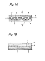
- Figure 1A is a cross section of part of the prior plasma display panel
- Figure 1B is a cross section on a line A-A of Figure 1A
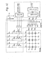
- Figure 1C is a circuit diagram for operating the plasma display panel of Figure 1A
- Figure 1D shows operational waveforms in the circuit of Figure 1C.
- a plurality of parallel column display electrodes 1 and a plurality of auxiliary seed electrodes 2 are mounted in elongate grooves provided in a back support panel 3.
- a plurality of row electrodes 4 is positioned perpendicular to the column electrodes 1 and the seed electrodes 2.
- a transparent cover glass 6 covers all the electrodes.
- the cover glass 6 has elongate grooves 5 which provide a discharge space, and opaque black masking portions 7 covering the seed electrodes 2.
- Each column electrode 1 is called an anode electrode
- each row electrode 4 is called a cathode electrode, since the former is coupled to an anode of a power source, and the latter is coupled to a cathode of a power source.
- anode electrodes Y 1 , Y 2 , Y 3 and seed electrodes S 1 , S 2 are positioned alternately so that they are perpendicular to cathode electrodes X i , X 2 , X 3 .
- the cathode electrodes X i , X 2 , X 3 are connected either to ground potential or to a predetermined potential V b by switches SX 1 , SX 2 , SX 3 , which are controlled by the output of a decoder.
- the decoder receives the output of a counter which receives clock pulses, and feeds control signals Tx 1 , T X2 , T x3 in sequence to the switches.
- the related cathode electrode X 1 , X 2 or X 3 is grounded.
- the anode electrodes Y 1 , Y 2 , Y 3 are coupled to a power source V a via resistors R 1 , and the junction point of each resistor R 1 and its respective anode electrode is grounded through a resistor R 2 and a switch SY 1 , SY 2 , SY 3 which is controlled by pattern data fed via a buffer circuit.
- Figure 1 D shows the operational time sequence of the circuit of Figure 1C.
- each frame period has three timing clock durations to, t 1 , t 2 , respectively.
- the cathode electrodes X 1 , X 2 , X 3 have applied thereto a respective potential V x1 , V x2 , V x3 , which is grounded alternately, as shown by the shaded areas in Figure 1D. Since the seed electrodes S 1 , S 2 always receive the high voltage V a via the resistors R 1 , a respective seed current I s1 , I s2 flows continuously as shown in Figure 1 D.
- the seed cell (X 1 ⁇ S 1 ) between the cathode electrode X 1 and the seed electrode S 1 is active, and current flows through that seed cell.
- the seed cell (X 1 -S 2 ) is active.
- the seed cells (X 2 ⁇ S 1 ) and (X 2 ⁇ S 2 ) are active.
- the seed cells (X 3 ⁇ S 1 ) and (X 3 ⁇ S 2 ) are active.
- the anode electrode Y 2 is at high voltage, and the other anode electrodes Y 1 and Y 3 are at low voltage. Therefore, only the cell (X 1 ⁇ Y 2 ) glows. It should be appreciated in that case that the seed cells (X 1 ⁇ S 1 ) and (X 1 -S 2 ) are active at the clock timing to, and there are many ions or charged particles around those active seed cells. Therefore, when the firing potential is applied to the display cell (X 1 ⁇ Y 2 ), that cell fires quickly due to the seed effect of the adjacent dimly glowing seed cells.
- the seed cells (X 1 -S 1 ) and (X 1 ⁇ S 2 ) turn off, but many charged ions remain around those cells. Therefore, when the potential is applied to the seed cells (X 2 ⁇ S 1 ) and (X 2 ⁇ S 2 ) which are located close to the seeds cells (X 1 ⁇ S 1 ) and (X 1 -S 2 ), the seed cells (X 2 -S 1 ) and (X 2 ⁇ S 2 ) fire quickly at the clock timing t 1 . Similarly, the display cells (X 2 ⁇ Y 1 ) and (X 2 -Y 2 ) fire quickly by the seed effect of the seed cells.
- the seed cells (X 3 ⁇ S 1 ) and (X 3 -S 2 ) and the display cell (X 3 -Y 3 ) fire.
- firing of the display cells is determined by the pattern data applied to the anode electrodes.
- the discharge of the seed cells shifts along the respective seed electrode, and similarly, the discharge of the display cells shifts along the anode electrode.
- Each selected display cell is fired quickly due to the presence of a seed cell.
- the prior plasma display panel as described has the disadvantage, due to the presence of the seed electrodes, that the density of the display cells cannot be high enough for good picture quality with high resolution. It should be noted that the space between the electrodes is restricted by the manufacturing process. If there were no seed electrodes, the spaces between the anode electrode could be halved, so the density of the anode electrodes could be doubled.
- the switching circuit further includes a second group of switches for selectively establishing a first or a second discharge current in each of the anode electrodes according to the picture pattern data, the first discharge current being sufficient to provide visible light due to the discharge and the second discharge current being lower than the first discharge current but sufficient to maintain a discharge when the first cathode potential is applied to the related cathode electrode, whereby the cells along a cathode electrode to which the first cathode potential is applied discharge with either the first discharge current or the second discharge current according to the picture pattern data, and provide excited seed particles for firing adjacent cells.
- a plurality of parallel column (anode) electrodes 12 1 to 12 " are mounted in elongate grooves provided in a back support plate 11.
- a plurality of row (cathode) electrodes 14 i to 14 " are positioned perpendicular to the column electrodes.
- the cross section of each cathode electrode is rectangular.
- a transparent cover glass plate 15 covers all of the electrodes.
- the cover plate 15 has a plurality of parallel elongate grooves 13" 1 to 13" n which provide a discharge space for the discharge cells.
- the grooves 13' 1 to 13' n which contain the anode electrodes 12 1 to 12 n also provide a discharge space.
- the discharge spaces are filled with a discharge gas, for instance neon or argon.
- a small quantity of mercury gas is also introduced into the discharge spaces for preventing damage to the cathode electrodes due to cathode-sputtering.
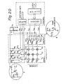
- Figure 2D shows a diagram of a circuit for operating the present plasma display panel
- Figure 2E shows the timing sequence of typical signals in the circuit of Figure 2D.
- the anode electrodes Y 1 , Y 2 , Y 3 are positioned perpendicular to the cathode electrodes X 1 , X 2 , X 3 .
- the cathode electrodes are connected either to ground potential or to the predetermined potential Vb through the switches SX 1 , SX 2 , SX 3 which are controlled by the output of the decoder.
- the decoder receives the output of the counter, which receives clock pulses CL, and the decoder applies control signals T x1 , T x2 , T x3 in sequence to the switches.
- each anode electrode Y 1 , Y 2 , Y 3 is coupled to the power source V a through a respective switch SY 1 , SY 2 , SY3 and one or other of resistors R 3 and R 4 . It is assumed that the , resistance of each resistor R 3 is higher than that of R 4 .
- Each resistor R 3 is for obtaining the seed discharge, and is preferably 500 kilo-ohms.
- Each resistor R 4 is for obtaining the display discharge and is preferably 50 kilo-ohms.
- each switch SY 1 , SY 2 , or SY 3 and the associated resistors R 3 and R 4 is shown in a circle A, in which the switch is implemented by a transistor O.
- the control signal T y1 applied to the base electrode of the transistor Q is inactive, the transistor Q is in the OFF state, and the anode electrode Y 1 is therefore supplied with the potential V a via the high-value resistor R 3 .
- the control signal T y1 when the control signal T y1 is active, the transistor Q is in the ON state, and the resistors R 3 and R 5 are connected in parallel with each other.
- the resistance of that parallel circuit is substantially the same as the resistance of R 4 . Accordingly, the anode electrode Y 1 is effectively coupled to the power potential V a through the resistor R 4 .
- the control signals T y1 , Ty 2 , and T y3 for controlling the switches SY 1 , SY 2 , SY 3 are supplied, via the buffer circuit, according to the pattern data to be displayed.
- each switch SX 1 , SX 2 , SX 3 is shown in a circle B, in which the switch is implemented by a transistor Q 1 .
- the switch is implemented by a transistor Q 1 .
- the transistor When the base electrode of the transistor Q 1 is inactive, the transistor is in the OFF state, and the related cathode electrode is therefore coupled to the potential V b , which is lower than the potential V a , via a resistor R. Hence, the related cathode electrode does not discharge.
- the base electrode of the transistor Q 1 when the base electrode of the transistor Q 1 is active, the transistor Q 1 is in the ON state, and the collector of that transistor is substantially grounded. The related cathode electrode is therefore also grounded. That cathode electrode discharges in this state.
- each transistor Q 1 switches the potential of the related cathode electrode between a first potential (ground potential) and a second potential (potential V b ).
- Each cell of the panel has two discharge modes, a seed discharge mode, and a display discharge mode.
- a cathode electrode When a cathode electrode is grounded, and an anode electrode is coupled to the power potential V a through the lower-value resistor R 4 , the cell defined by the crossing point of that cathode electrode and that anode electrode discharges strongly, and the discharge is visible for display purposes.
- the cell when a cathode electrode is grounded, and an anode electrode is coupled to the power potential V a through the high-value resistor R 3 , the cell discharges weakly. The weak discharge is not visible, because the discharge light is masked by the cathode electrode itself. That weak discharge is used as a seed discharge.
- the strong discharge for display purposes is called herein a first mode discharge, and the weak seed discharge is called a second mode discharge.
- Figure 2E shows the operational time sequence of the circuit of Figure 2D. It is assumed that each frame period has three timing clock durations to, t 1 , t 2 .
- the cathode electrodes X 1 , X 2 , X 3 have applied thereto the respective potentials V x1 , V x2 , V x3 which are grounded in sequence as shown by the shaded areas in Figure 2E.
- the control potential V x1 is grounded, so that the cathode electrode X 1 is grounded.
- the cells (X 1 ⁇ Y 1 ), (X 1 ⁇ Y 2 ) and (X 1 ⁇ Y 3 ) which relate to the first cathode electrode X 1 discharge at least weakly. Furthermore, if any of the anode electrodes are switched so that the lower-value resistors R 4 are effective, the cells defined by the first cathode electrode X 1 and the anode electrodes with the low-value resistors discharge strongly for display purposes.
- the control potential V x1 is at V b
- the control potential V X2 is at ground. Therefore, the cells relating to the cathode electrode X 1 no longer discharge, and the cells (X 2 ⁇ Y 1 ), (X 2 ⁇ Y 2 ) and (X 2 ⁇ Y 3 ), relating to the second cathode electrode X 2 , discharge either weakly or strongly.
- the current l y1 and the current ly 2 are at high level, and therefore the cells (X 2 -Y 1 ) and (X 2 ⁇ Y 2 ) discharge strongly for display purposes, and the cell (X 2 -Y 3 ) discharges weakly to act as a seed cell.
- the discharge from the first cathode electrode X to the second cathode electrode X 2 along the anode electrodes, it should be appreciated that the charged ions around the first cathode electrode X 1 function as seeds for firing the cells on the second cathode electrode X 2 . Therefore, the firing of a new cell is accomplished in a very short time, due to the seed effect of the previously discharged cells, although no specific seed electrode is provided.
- the discharge along the second cathode electrode X 2 transfers to the third cathode electrode X 3 . Therefore, the discharge scans along the anode electrodes.
- the current l y3 is high, so the cell (X 3 -Y 3 ) is bright and the other cells (X 3 ⁇ Y 1 ) and (X 3 -Y 2 ) are dark.
- the above operations are repeated by transferring the discharge cell position along the anode electrodes. Accordingly, in the embodiment of Figures 2D and 2E, the cells (X 1 ⁇ Y 2 ), (X 2 ⁇ Y 1 ), (X Z -Y 2 ), and (X 3 -Y 3 ) are bright and discharge strongly for display purposes, as shown by the shaded dots in Figure 2D, and the other cells discharge weakly, merely for seed purposes.
- the first clock duration might be longer than other clock durations.
- the clock durations might be uniform, and an additional hidden seed electrode, as described in US patent No. 3 644 925, might be provided near the first cathode electrode X,.
- the present plasma display panel has no specific seed electrode, and all the electrodes, and the cells defined by the electrodes, are used as display cells. Therefore, the density of the cells, or the resolution power of a picture thus displayed, is doubled as compared with that of the prior plasma display panel, and a good quality picture is displayed.
- the quick firing, or high speed scanning, of the prior plasma display panel which has seed electrodes is also obtained in the present invention.
- the present plasma display panel provides a visible pattern due to the bright light passing through the cathode electrodes, but the seed discharge is not visible, because the dim light produced by the seed discharge is hidden by the cathode electrodes. Hence, no cover for masking the seed discharge light is necessary in the present invention.
Landscapes
- Control Of Indicators Other Than Cathode Ray Tubes (AREA)
- Gas-Filled Discharge Tubes (AREA)
Claims (8)
Applications Claiming Priority (2)
| Application Number | Priority Date | Filing Date | Title |
|---|---|---|---|
| JP208354/83 | 1983-11-08 | ||
| JP58208354A JPS60101595A (ja) | 1983-11-08 | 1983-11-08 | プラズマ・デイスプレイ装置の駆動方式 |
Publications (3)
| Publication Number | Publication Date |
|---|---|
| EP0141669A2 EP0141669A2 (de) | 1985-05-15 |
| EP0141669A3 EP0141669A3 (en) | 1986-02-19 |
| EP0141669B1 true EP0141669B1 (de) | 1989-08-02 |
Family
ID=16554894
Family Applications (1)
| Application Number | Title | Priority Date | Filing Date |
|---|---|---|---|
| EP84307642A Expired EP0141669B1 (de) | 1983-11-08 | 1984-11-06 | Aufzeichnungspaneelsystem |
Country Status (4)
| Country | Link |
|---|---|
| US (1) | US4633139A (de) |
| EP (1) | EP0141669B1 (de) |
| JP (1) | JPS60101595A (de) |
| DE (1) | DE3479267D1 (de) |
Families Citing this family (5)
| Publication number | Priority date | Publication date | Assignee | Title |
|---|---|---|---|---|
| JPS62171385A (ja) * | 1986-01-24 | 1987-07-28 | Mitsubishi Electric Corp | 中間調表示方式 |
| US5469021A (en) * | 1993-06-02 | 1995-11-21 | Btl Fellows Company, Llc | Gas discharge flat-panel display and method for making the same |
| US5954560A (en) * | 1993-06-02 | 1999-09-21 | Spectron Corporation Of America, L.L.C. | Method for making a gas discharge flat-panel display |
| TW544701B (en) * | 2001-01-29 | 2003-08-01 | Technology Trade & Transfer | Flat discharge display device |
| FR2896610A1 (fr) * | 2006-01-20 | 2007-07-27 | St Microelectronics Sa | Procede et dispositif de commande d'un ecran a plasma matriciel |
Family Cites Families (12)
| Publication number | Priority date | Publication date | Assignee | Title |
|---|---|---|---|---|
| US3644925A (en) * | 1969-01-07 | 1972-02-22 | Burroughs Corp | Gaseous discharge display panel with auxiliary excitation cells |
| US3619698A (en) * | 1970-02-05 | 1971-11-09 | Burroughs Corp | Display panel |
| US3626235A (en) * | 1970-03-13 | 1971-12-07 | Burroughs Corp | Display panel with double cathode |
| US3626245A (en) * | 1970-04-08 | 1971-12-07 | Burroughs Corp | Display panel having a plurality of display registers |
| NL7204576A (de) * | 1972-04-06 | 1973-10-09 | ||
| USRE29858E (en) * | 1975-12-02 | 1978-12-05 | Burroughs Corporation | Display panel |
| JPS5926103B2 (ja) * | 1978-07-14 | 1984-06-23 | 松下電子工業株式会社 | 気体放電形表示装置 |
| US4278918A (en) * | 1980-03-31 | 1981-07-14 | Modern Controls, Inc. | Display panel driver circuit |
| US4349816A (en) * | 1981-03-27 | 1982-09-14 | The United States Of America As Represented By The Secretary Of The Army | Drive circuit for matrix displays |
| JPS57162692U (de) * | 1981-04-03 | 1982-10-13 | ||
| US4373157A (en) * | 1981-04-29 | 1983-02-08 | Burroughs Corporation | System for operating a display panel |
| JPS5836792A (ja) * | 1981-08-26 | 1983-03-03 | Mitsubishi Heavy Ind Ltd | スラリ濃度調整タンク付きスラリ船 |
-
1983
- 1983-11-08 JP JP58208354A patent/JPS60101595A/ja active Pending
-
1984
- 1984-10-30 US US06/666,338 patent/US4633139A/en not_active Expired - Fee Related
- 1984-11-06 DE DE8484307642T patent/DE3479267D1/de not_active Expired
- 1984-11-06 EP EP84307642A patent/EP0141669B1/de not_active Expired
Also Published As
| Publication number | Publication date |
|---|---|
| DE3479267D1 (en) | 1989-09-07 |
| EP0141669A3 (en) | 1986-02-19 |
| US4633139A (en) | 1986-12-30 |
| JPS60101595A (ja) | 1985-06-05 |
| EP0141669A2 (de) | 1985-05-15 |
Similar Documents
| Publication | Publication Date | Title |
|---|---|---|
| US6313580B1 (en) | AC-discharge type plasma display panel and method for driving the same | |
| US5075597A (en) | Method for the row-by-row control of a coplanar sustaining ac type of plasma panel | |
| EP0545642B1 (de) | Entladungs-Anzeigeröhren | |
| KR100657384B1 (ko) | 플라즈마 디스플레이 패널의 구동방법 | |
| KR20020077015A (ko) | Ac형 pdp의 구동 방법 및 구동 장치 | |
| EP0138329B1 (de) | Einrichtung und Verfahren zur Steuerung einer Anzeigeeinrichtung mit Speichereigenschaft | |
| JPS63309994A (ja) | 1画素につき4つの電極を有するプラズマディスプレイパネルとその制御方法 | |
| EP0141669B1 (de) | Aufzeichnungspaneelsystem | |
| EP0023082B1 (de) | Anzeigevorrichtung und Verfahren in ihrem Betrieb | |
| US4513281A (en) | AC plasma panel shift with intensity control | |
| US4613854A (en) | System for operating a dot matrix display panel to prevent crosstalk | |
| US6052160A (en) | Display device with sputter-resistant electrode layer for providing plasma discharge | |
| KR100679440B1 (ko) | 교류형 플라즈마표시패널의 구동방법 | |
| US4532505A (en) | Gas-filled dot matrix display panel | |
| GB1585386A (en) | Driving and addressing circuitry for gas discharge display/memory device | |
| KR20010005890A (ko) | 플라즈마 표시장치 및 구동 방법 | |
| US4336535A (en) | Cursor for plasma shift register display | |
| EP0122072B1 (de) | Gasgefüllte Punkt-Matrix-Anzeigeeinheit und Betriebssystem | |
| US4010395A (en) | Gas discharge display panel with cell-firing means having glow spreading electrode | |
| CA1233920A (en) | Method and system for operating a display panel having memory | |
| US4047169A (en) | Display panel having improved arrangement of reset cells for facilitating scanning of the panel | |
| US4039881A (en) | Plasma display screen for displaying a matrix of luminous points | |
| JPH0142104B2 (de) | ||
| KR100810483B1 (ko) | 플라즈마 디스플레이 패널의 구동 방법, 플라즈마디스플레이 패널 및 플라즈마 표시 장치 | |
| Weston | Gas discharge data displays |
Legal Events
| Date | Code | Title | Description |
|---|---|---|---|
| PUAI | Public reference made under article 153(3) epc to a published international application that has entered the european phase |
Free format text: ORIGINAL CODE: 0009012 |
|
| 17P | Request for examination filed |
Effective date: 19841120 |
|
| AK | Designated contracting states |
Designated state(s): DE FR GB NL |
|
| PUAL | Search report despatched |
Free format text: ORIGINAL CODE: 0009013 |
|
| AK | Designated contracting states |
Designated state(s): DE FR GB NL |
|
| 17Q | First examination report despatched |
Effective date: 19871204 |
|
| GRAA | (expected) grant |
Free format text: ORIGINAL CODE: 0009210 |
|
| AK | Designated contracting states |
Kind code of ref document: B1 Designated state(s): DE FR GB NL |
|
| REF | Corresponds to: |
Ref document number: 3479267 Country of ref document: DE Date of ref document: 19890907 |
|
| ET | Fr: translation filed | ||
| PLBE | No opposition filed within time limit |
Free format text: ORIGINAL CODE: 0009261 |
|
| STAA | Information on the status of an ep patent application or granted ep patent |
Free format text: STATUS: NO OPPOSITION FILED WITHIN TIME LIMIT |
|
| 26N | No opposition filed | ||
| PGFP | Annual fee paid to national office [announced via postgrant information from national office to epo] |
Ref country code: FR Payment date: 19920924 Year of fee payment: 9 |
|
| PGFP | Annual fee paid to national office [announced via postgrant information from national office to epo] |
Ref country code: GB Payment date: 19921026 Year of fee payment: 9 |
|
| PGFP | Annual fee paid to national office [announced via postgrant information from national office to epo] |
Ref country code: DE Payment date: 19921119 Year of fee payment: 9 |
|
| PGFP | Annual fee paid to national office [announced via postgrant information from national office to epo] |
Ref country code: NL Payment date: 19921130 Year of fee payment: 9 |
|
| PG25 | Lapsed in a contracting state [announced via postgrant information from national office to epo] |
Ref country code: GB Effective date: 19931106 |
|
| PG25 | Lapsed in a contracting state [announced via postgrant information from national office to epo] |
Ref country code: NL Effective date: 19940601 |
|
| GBPC | Gb: european patent ceased through non-payment of renewal fee |
Effective date: 19931106 |
|
| NLV4 | Nl: lapsed or anulled due to non-payment of the annual fee | ||
| PG25 | Lapsed in a contracting state [announced via postgrant information from national office to epo] |
Ref country code: FR Effective date: 19940729 |
|
| PG25 | Lapsed in a contracting state [announced via postgrant information from national office to epo] |
Ref country code: DE Effective date: 19940802 |
|
| REG | Reference to a national code |
Ref country code: FR Ref legal event code: ST |