EP0141999A1 - Verfahren zur Herstellung eines polykristallinen Stabes aus Halbleitermaterial - Google Patents
Verfahren zur Herstellung eines polykristallinen Stabes aus Halbleitermaterial Download PDFInfo
- Publication number
- EP0141999A1 EP0141999A1 EP84111751A EP84111751A EP0141999A1 EP 0141999 A1 EP0141999 A1 EP 0141999A1 EP 84111751 A EP84111751 A EP 84111751A EP 84111751 A EP84111751 A EP 84111751A EP 0141999 A1 EP0141999 A1 EP 0141999A1
- Authority
- EP
- European Patent Office
- Prior art keywords
- crucible
- wall
- semiconductor material
- bath
- solidification
- Prior art date
- Legal status (The legal status is an assumption and is not a legal conclusion. Google has not performed a legal analysis and makes no representation as to the accuracy of the status listed.)
- Granted
Links
Images

Classifications
-
- C—CHEMISTRY; METALLURGY
- C30—CRYSTAL GROWTH
- C30B—SINGLE-CRYSTAL GROWTH; UNIDIRECTIONAL SOLIDIFICATION OF EUTECTIC MATERIAL OR UNIDIRECTIONAL DEMIXING OF EUTECTOID MATERIAL; REFINING BY ZONE-MELTING OF MATERIAL; PRODUCTION OF A HOMOGENEOUS POLYCRYSTALLINE MATERIAL WITH DEFINED STRUCTURE; SINGLE CRYSTALS OR HOMOGENEOUS POLYCRYSTALLINE MATERIAL WITH DEFINED STRUCTURE; AFTER-TREATMENT OF SINGLE CRYSTALS OR A HOMOGENEOUS POLYCRYSTALLINE MATERIAL WITH DEFINED STRUCTURE; APPARATUS THEREFOR
- C30B11/00—Single-crystal growth by normal freezing or freezing under temperature gradient, e.g. Bridgman-Stockbarger method
- C30B11/007—Mechanisms for moving either the charge or the heater
-
- C—CHEMISTRY; METALLURGY
- C30—CRYSTAL GROWTH
- C30B—SINGLE-CRYSTAL GROWTH; UNIDIRECTIONAL SOLIDIFICATION OF EUTECTIC MATERIAL OR UNIDIRECTIONAL DEMIXING OF EUTECTOID MATERIAL; REFINING BY ZONE-MELTING OF MATERIAL; PRODUCTION OF A HOMOGENEOUS POLYCRYSTALLINE MATERIAL WITH DEFINED STRUCTURE; SINGLE CRYSTALS OR HOMOGENEOUS POLYCRYSTALLINE MATERIAL WITH DEFINED STRUCTURE; AFTER-TREATMENT OF SINGLE CRYSTALS OR A HOMOGENEOUS POLYCRYSTALLINE MATERIAL WITH DEFINED STRUCTURE; APPARATUS THEREFOR
- C30B11/00—Single-crystal growth by normal freezing or freezing under temperature gradient, e.g. Bridgman-Stockbarger method
- C30B11/003—Heating or cooling of the melt or the crystallised material
Definitions
- the surface of the bottom portion of the crucible in contact with the exchanger is necessarily small compared to the total surface of the bottom of the crucible so as not to harm the melting of the sample. This results in a low solidification speed, the total duration of solidification being of the order of approximately 15 to 25 hours.
- the isotherms of the molten material bath have substantially a hemispherical shape centered on the contact surface.
- this material is silicon intended for the manufacture of solar cells
- the ingots obtained by this process have a hemispherical polycrystalline structure, which is, in principle, unfavorable for obtaining good photovoltaic characteristics of the material.
- the solidification step successively comprises a first period in which the flow of helium is increased as well as the heating power and a second period in which the flow of helium is continued to increase by decreasing the heating power.
- the passage from the first to the second period takes place at a time when the bath is partially solidified.
- the present invention aims to overcome these drawbacks.
- the insulated chamber comprising a removable bottom wall covering most of the bottom of the crucible, the l heat energy at the bottom of the crucible by removing said bottom wall, the power of said heating being maintained at a constant level throughout the solidification step, this level being that which makes it possible to obtain said constant temperature of the bath at the end of the 'heating stage.
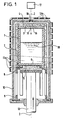
- FIGS 1 and 2 is shown a graphite crucible 1, arranged vertically along a vertical axis 2.
- the upper opening of the crucible 1 is closed by a removable horizontal cover 3, also in graphite.
- the crucible 1 is placed in an insulated chamber whose walls, made of graphite felt, completely surround the crucible and are applied directly to its outer surface and to the cover. These walls include a horizontal upper wall 4 covering the cover 3, a removable lower wall 5 applied to the bottom 6 of the crucible and covering most of the surface of this bottom, and a vertical tubular wall 7 applied to the lateral surface of the crucible .
- the wall 7 has a horizontal lower extension 8 advancing towards the axis 2, to support the edges of the bottom 6 of the crucible 1 when the wall 5 is removed.
- the insulated chamber is raised by a graphite support 9 which rests on the bottom of an enclosure 10 made of an electrically insulating material, this enclosure surrounding the support 9 and the insulated chamber.
- an electrical winding which comprises a helical part 11 surrounding the upper part of the lateral surface of the enclosure 10 and a planar part 12 disposed above the upper face of this enclosure.
- the removable bottom wall 5 of the heat-insulated chamber is fixed to the upper end of a vertical rod 13 which crosses tightly, along the axis 2, the bottom of the enclosure 10.
- the cover 3 and the wall 4 comprise respectively two small central openings 14 and 15 and the upper face of the enclosure 10 is provided with a small transparent window 16 arranged along the axis 2 opposite the openings 14 and 15.
- An optical pyrometer 17 is placed on the axis 2 outside enclosure 10 in front of window 16.
- the windings 11 and 12 are connected to an electrical source at medium frequency, not shown, so as to induce in the walls of the crucible 1 and in its cover 3 an electric current which gives off enough heat to melt the silicon placed in the crucible.
- the presence of an inert atmosphere in the enclosure 10 prevents any combustion of the crucible, its cover, the support 9 and the carbon felt constituting the walls of the heat-insulated chamber.
- a bath 18 of molten silicon is obtained and the electrical supply of the windings 11 and 12 is adjusted to a level making it possible to maintain this bath at a constant temperature slightly higher than the melting temperature of silicon.
- the entire device then conforms to what is shown in FIG. 1, the crucible 1, the cover 3, the windings 11 and 12 and the heat-insulated chamber constituting an induction furnace.
- the rod control system 13 is then actuated so as to cause the rod to move up and down along axis 2, while maintaining the power supply to the oven at the level allowing, at the end of the 'previous step, to maintain constant the temperature of the bath at a value slightly higher than that of the silicon fusion.
- the wall 5 of the heat-insulated chamber is then lowered so as to occupy the position indicated in FIG. 2.
- the bottom of the crucible thus uncovered removes part of its heat energy by radiation. This results in crystallization of the silicon, which begins at the bottom of the crucible 1 and gradually propagates towards the surface of the bath. Throughout this solidification step, the power supply power of the oven remains constant, at the same level as that where it was set at the end of the previous step.
- FIG. 2 represents the device during the solidification step, when a mass of solidified silicon 19 has formed in the bath 18. It can be seen that the separation surface between the solid and liquid silicon is substantially horizontal; it is possible to verify that the isotherms of the bath 18 remain horizontal during the solidification step.
- the temperature of the bath is stabilized at 1430 ° C.
- the crystallization is triggered by opening a 300 cm 2 orifice made in the part of the heat-insulated chamber which covers the bottom of the crucible. the crystallization time is approximately 4 hours.
- a batch of solar cells was produced by cutting the ingot thus obtained into slices with a thickness of 450 micrometers and an area of 100 cm 2 .
- a photovoltaic yield of 10.3% was measured on a selection of the best cells in the batch, this selection representing 10% of the cells.
Landscapes
- Chemical & Material Sciences (AREA)
- Engineering & Computer Science (AREA)
- Crystallography & Structural Chemistry (AREA)
- Materials Engineering (AREA)
- Metallurgy (AREA)
- Organic Chemistry (AREA)
- Silicon Compounds (AREA)
- Crystals, And After-Treatments Of Crystals (AREA)
- Crucibles And Fluidized-Bed Furnaces (AREA)
- Liquid Deposition Of Substances Of Which Semiconductor Devices Are Composed (AREA)
Applications Claiming Priority (2)
| Application Number | Priority Date | Filing Date | Title |
|---|---|---|---|
| FR8315868 | 1983-10-05 | ||
| FR8315868A FR2553232B1 (fr) | 1983-10-05 | 1983-10-05 | Procede et dispositif pour elaborer un lingot d'un materiau semi-conducteur polycristallin |
Publications (2)
| Publication Number | Publication Date |
|---|---|
| EP0141999A1 true EP0141999A1 (de) | 1985-05-22 |
| EP0141999B1 EP0141999B1 (de) | 1987-05-27 |
Family
ID=9292851
Family Applications (1)
| Application Number | Title | Priority Date | Filing Date |
|---|---|---|---|
| EP84111751A Expired EP0141999B1 (de) | 1983-10-05 | 1984-10-02 | Verfahren zur Herstellung eines polykristallinen Stabes aus Halbleitermaterial |
Country Status (5)
| Country | Link |
|---|---|
| EP (1) | EP0141999B1 (de) |
| JP (1) | JPS60103017A (de) |
| CA (1) | CA1260363A (de) |
| DE (1) | DE3463951D1 (de) |
| FR (1) | FR2553232B1 (de) |
Cited By (9)
| Publication number | Priority date | Publication date | Assignee | Title |
|---|---|---|---|---|
| EP0186249A3 (en) * | 1984-12-21 | 1989-07-05 | Pragma S.P.A. | Process for the preparation of polycrystalline materials and equipment suitable to the accomplishing thereof |
| EP0939146A1 (de) * | 1998-02-25 | 1999-09-01 | Mitsubishi Materials Corporation | Verfahren und Vorrichtung zur Herstellung eines Siliciumstabes mit einer Struktur hergestellt durch gerichtete Erstarrung |
| DE19855061A1 (de) * | 1998-11-28 | 2000-05-31 | Ald Vacuum Techn Ag | Schmelzofen zum Schmelzen von Silizium |
| US6640876B2 (en) | 2000-06-07 | 2003-11-04 | Mitsubishi Materials Corporation | Method and apparatus for manufacturing copper and/or copper alloy ingot having no shrinkage cavity and having smooth surface without wrinkles |
| EP1754807A3 (de) * | 2005-08-18 | 2008-12-24 | BP Corporation North America Inc. | Isolierpaket-Anordnung für die Anwendung in Hochtemperaturöfen |
| EP2014803A1 (de) * | 2007-07-10 | 2009-01-14 | Commissariat à l'Energie Atomique | Vorrichtung zur Herstellung eines Blocks aus kristallinem Material mit Modulation der Wärmeleitfähigkeit |
| KR101240001B1 (ko) * | 2008-09-29 | 2013-03-06 | 실버브룩 리서치 피티와이 리미티드 | 효율적인 잉크젯 노즐 조립체 |
| KR101270371B1 (ko) * | 2008-05-05 | 2013-06-05 | 실버브룩 리서치 피티와이 리미티드 | 저항 가열 바아를 갖는 굽은 능동 빔을 포함하는 서멀 벤드 액츄에이터 |
| EP3066235B1 (de) * | 2013-11-07 | 2019-05-01 | EBNER Industrieofenbau GmbH | Regelung der temperatur eines tiegels in einem ofen |
Families Citing this family (5)
| Publication number | Priority date | Publication date | Assignee | Title |
|---|---|---|---|---|
| JP2006282495A (ja) * | 2005-03-10 | 2006-10-19 | Kyocera Corp | 鋳型及びこれを用いた多結晶シリコンインゴットの製造方法 |
| JP2006335582A (ja) * | 2005-05-31 | 2006-12-14 | Daiichi Kiden:Kk | 結晶シリコン製造装置とその製造方法 |
| FR2940327B1 (fr) | 2008-12-19 | 2011-02-11 | Commissariat Energie Atomique | Four de fusion-solidification comportant une modulation des echanges thermiques par les parois laterales |
| DE102009015113A1 (de) * | 2009-03-31 | 2010-10-14 | Schott Ag | Vorrichtung und Verfahren zur Züchtung von Kristallen |
| CN110170637B (zh) * | 2019-05-28 | 2021-05-25 | 深圳市万泽中南研究院有限公司 | 一种保持铸件定向凝固过程稳定性的设备与工艺 |
Citations (2)
| Publication number | Priority date | Publication date | Assignee | Title |
|---|---|---|---|---|
| FR2255950A1 (de) * | 1973-12-28 | 1975-07-25 | Crystal Syst | |
| US4015657A (en) * | 1975-09-03 | 1977-04-05 | Dmitry Andreevich Petrov | Device for making single-crystal products |
-
1983
- 1983-10-05 FR FR8315868A patent/FR2553232B1/fr not_active Expired
-
1984
- 1984-10-02 EP EP84111751A patent/EP0141999B1/de not_active Expired
- 1984-10-02 CA CA000464545A patent/CA1260363A/fr not_active Expired
- 1984-10-02 DE DE8484111751T patent/DE3463951D1/de not_active Expired
- 1984-10-03 JP JP59207934A patent/JPS60103017A/ja active Granted
Patent Citations (2)
| Publication number | Priority date | Publication date | Assignee | Title |
|---|---|---|---|---|
| FR2255950A1 (de) * | 1973-12-28 | 1975-07-25 | Crystal Syst | |
| US4015657A (en) * | 1975-09-03 | 1977-04-05 | Dmitry Andreevich Petrov | Device for making single-crystal products |
Cited By (14)
| Publication number | Priority date | Publication date | Assignee | Title |
|---|---|---|---|---|
| EP0186249A3 (en) * | 1984-12-21 | 1989-07-05 | Pragma S.P.A. | Process for the preparation of polycrystalline materials and equipment suitable to the accomplishing thereof |
| EP0939146A1 (de) * | 1998-02-25 | 1999-09-01 | Mitsubishi Materials Corporation | Verfahren und Vorrichtung zur Herstellung eines Siliciumstabes mit einer Struktur hergestellt durch gerichtete Erstarrung |
| US6299682B1 (en) | 1998-02-25 | 2001-10-09 | Mitsubishi Materials Corporation | Method for producing silicon ingot having directional solidification structure and apparatus for producing the same |
| US6378835B1 (en) | 1998-02-25 | 2002-04-30 | Mitsubishi Materials Corporation | Method for producing silicon ingot having directional solidification structure and apparatus for producing the same |
| DE19855061B4 (de) * | 1998-11-28 | 2012-05-16 | Ald Vacuum Technologies Ag | Schmelzofen zum Schmelzen von Silizium |
| DE19855061A1 (de) * | 1998-11-28 | 2000-05-31 | Ald Vacuum Techn Ag | Schmelzofen zum Schmelzen von Silizium |
| US6640876B2 (en) | 2000-06-07 | 2003-11-04 | Mitsubishi Materials Corporation | Method and apparatus for manufacturing copper and/or copper alloy ingot having no shrinkage cavity and having smooth surface without wrinkles |
| EP1754807A3 (de) * | 2005-08-18 | 2008-12-24 | BP Corporation North America Inc. | Isolierpaket-Anordnung für die Anwendung in Hochtemperaturöfen |
| FR2918675A1 (fr) * | 2007-07-10 | 2009-01-16 | Commissariat Energie Atomique | Dispositif de fabrication d'un bloc de materiau cristallin avec modulation de la conductivite thermique. |
| US8172944B2 (en) | 2007-07-10 | 2012-05-08 | Commissariat A L'energie Atomique | Device for producing a block of crystalline material with modulation of the thermal conductivity |
| EP2014803A1 (de) * | 2007-07-10 | 2009-01-14 | Commissariat à l'Energie Atomique | Vorrichtung zur Herstellung eines Blocks aus kristallinem Material mit Modulation der Wärmeleitfähigkeit |
| KR101270371B1 (ko) * | 2008-05-05 | 2013-06-05 | 실버브룩 리서치 피티와이 리미티드 | 저항 가열 바아를 갖는 굽은 능동 빔을 포함하는 서멀 벤드 액츄에이터 |
| KR101240001B1 (ko) * | 2008-09-29 | 2013-03-06 | 실버브룩 리서치 피티와이 리미티드 | 효율적인 잉크젯 노즐 조립체 |
| EP3066235B1 (de) * | 2013-11-07 | 2019-05-01 | EBNER Industrieofenbau GmbH | Regelung der temperatur eines tiegels in einem ofen |
Also Published As
| Publication number | Publication date |
|---|---|
| FR2553232A1 (fr) | 1985-04-12 |
| FR2553232B1 (fr) | 1985-12-27 |
| EP0141999B1 (de) | 1987-05-27 |
| CA1260363A (fr) | 1989-09-26 |
| JPS6256083B2 (de) | 1987-11-24 |
| DE3463951D1 (en) | 1987-07-02 |
| JPS60103017A (ja) | 1985-06-07 |
Similar Documents
| Publication | Publication Date | Title |
|---|---|---|
| EP0141999B1 (de) | Verfahren zur Herstellung eines polykristallinen Stabes aus Halbleitermaterial | |
| US4282184A (en) | Continuous replenishment of molten semiconductor in a Czochralski-process, single-crystal-growing furnace | |
| EP2014803B1 (de) | Vorrichtung zur Herstellung eines Blocks aus kristallinem Material mit Modulation der Wärmeleitfähigkeit | |
| CA1128732A (fr) | Procede et dispositif d'elaboration de silicium polycristallin | |
| EP0275228B1 (de) | Verfahren und Anlage zum Schmelzen und Stranggiessen von Metallen | |
| FR2511708A1 (fr) | Procede et appareil pour regler l'atmosphere entourant une zone de croissance cristalline | |
| EP0130865B1 (de) | Vorrichtung zur Herstellung eines Einkristalls | |
| JP2010504905A (ja) | 結晶シリコン基板を製造するための方法及び装置 | |
| FR2501354A1 (fr) | Four electrique pour la fusion d'une charge non homogene et le melange de la matiere fondue, et procede pour optimiser la fusion d'un oxyde et melanger l'oxyde | |
| JPH107493A (ja) | シリコン半導体基板および太陽電池用基板の製造方法 | |
| FR2526449A1 (fr) | Procede et dispositif de fabrication d'un monocristal, exempt de toute contrainte, d'un compose ferroelectrique a structure cristalline | |
| FR2979357A1 (fr) | Systeme de fabrication d'un materiau cristallin par cristallisation dirigee muni d'une source de chaleur additionnelle laterale | |
| FR2569430A1 (fr) | Appareil pour extraire des monocristaux d'un bain de materiau semi-conducteur fondu contenu dans un creuset | |
| JP2007015905A (ja) | 多結晶シリコンインゴット、多結晶シリコン基板、並びに太陽電池素子および多結晶シリコンインゴットの鋳造方法。 | |
| EP3475012B1 (de) | Kühlofen mit gerichteter erstarrung und kühlverfahren mit solch einem ofen | |
| JP4534022B2 (ja) | Gaドープ結晶シリコン、その製造方法及びその製造方法に用いるGaドープ結晶シリコン製造装置、並びにGaドープ結晶シリコン基板を用いた太陽電池及びその製造方法 | |
| EP0775766A1 (de) | Kristallisationsofen zur Herstellung eines Stoffes mit niedriger Wärmgleitfähigkeit und/oder niedriger Härte | |
| EP0214350B1 (de) | Verfahren zur Herstellung einer polykristallinen Legierung zum Züchten von Einkristallen durch Durchgang in eine Lösungszone | |
| EP0768017B1 (de) | Ofen und herstellungsverfahren für geschmolzene erzeugnisse | |
| JP2010030868A (ja) | 半導体単結晶の製造方法 | |
| FR2927910A1 (fr) | Procede de cristallogenese d'un materiau electriquement conducteur a l'etat fondu. | |
| FR2509638A1 (fr) | Moule et procede pour le moulage de lingots de silicium destines a etre utilises comme materiau pour la realisation de cellules solaires | |
| JP4188725B2 (ja) | 板状シリコンの製造方法、板状シリコン製造用下地板、板状シリコンおよび該板状シリコンを用いた太陽電池 | |
| EP3727725B1 (de) | Tiegel für direktierte solidifikation | |
| BE450574A (de) |
Legal Events
| Date | Code | Title | Description |
|---|---|---|---|
| PUAI | Public reference made under article 153(3) epc to a published international application that has entered the european phase |
Free format text: ORIGINAL CODE: 0009012 |
|
| AK | Designated contracting states |
Designated state(s): BE CH DE FR GB IT LI NL SE |
|
| 17P | Request for examination filed |
Effective date: 19851114 |
|
| 17Q | First examination report despatched |
Effective date: 19860801 |
|
| GRAA | (expected) grant |
Free format text: ORIGINAL CODE: 0009210 |
|
| AK | Designated contracting states |
Kind code of ref document: B1 Designated state(s): BE CH DE FR GB IT LI NL SE |
|
| REF | Corresponds to: |
Ref document number: 3463951 Country of ref document: DE Date of ref document: 19870702 |
|
| ITF | It: translation for a ep patent filed | ||
| PLBE | No opposition filed within time limit |
Free format text: ORIGINAL CODE: 0009261 |
|
| STAA | Information on the status of an ep patent application or granted ep patent |
Free format text: STATUS: NO OPPOSITION FILED WITHIN TIME LIMIT |
|
| 26N | No opposition filed | ||
| ITTA | It: last paid annual fee | ||
| REG | Reference to a national code |
Ref country code: GB Ref legal event code: 732E |
|
| REG | Reference to a national code |
Ref country code: FR Ref legal event code: TP Ref country code: FR Ref legal event code: CD |
|
| REG | Reference to a national code |
Ref country code: CH Ref legal event code: PUE Owner name: PHOTOWATT INTERNATIONAL S.A. Ref country code: CH Ref legal event code: PFA Free format text: ALCATEL ALSTHOM COMPAGNIE GENERALE D'ELECTRICITE |
|
| ITPR | It: changes in ownership of a european patent |
Owner name: CESSIONE;PHOTOWATT INTERNATIONAL S.A. |
|
| NLT1 | Nl: modifications of names registered in virtue of documents presented to the patent office pursuant to art. 16 a, paragraph 1 |
Owner name: ALCATEL ALSTHOM COMPAGNIE GENERALE D'ELECTRICITE T |
|
| NLS | Nl: assignments of ep-patents |
Owner name: PHOTOWATT INTERNATIONAL S.A. TE BOURGOIN JALLIEU, |
|
| PGFP | Annual fee paid to national office [announced via postgrant information from national office to epo] |
Ref country code: NL Payment date: 19941031 Year of fee payment: 11 |
|
| BECH | Be: change of holder |
Free format text: 940126 S.A. *PHOTOWATT INTERNATIONAL |
|
| EAL | Se: european patent in force in sweden |
Ref document number: 84111751.8 |
|
| PGFP | Annual fee paid to national office [announced via postgrant information from national office to epo] |
Ref country code: GB Payment date: 19950814 Year of fee payment: 12 |
|
| PGFP | Annual fee paid to national office [announced via postgrant information from national office to epo] |
Ref country code: SE Payment date: 19950918 Year of fee payment: 12 Ref country code: DE Payment date: 19950918 Year of fee payment: 12 |
|
| PGFP | Annual fee paid to national office [announced via postgrant information from national office to epo] |
Ref country code: BE Payment date: 19950926 Year of fee payment: 12 |
|
| PG25 | Lapsed in a contracting state [announced via postgrant information from national office to epo] |
Ref country code: NL Effective date: 19960501 |
|
| NLV4 | Nl: lapsed or anulled due to non-payment of the annual fee |
Effective date: 19960501 |
|
| PG25 | Lapsed in a contracting state [announced via postgrant information from national office to epo] |
Ref country code: GB Effective date: 19961002 |
|
| PG25 | Lapsed in a contracting state [announced via postgrant information from national office to epo] |
Ref country code: SE Effective date: 19961003 |
|
| PG25 | Lapsed in a contracting state [announced via postgrant information from national office to epo] |
Ref country code: BE Effective date: 19961031 |
|
| BERE | Be: lapsed |
Owner name: S.A. PHOTOWATT INTERNATIONAL Effective date: 19961031 |
|
| GBPC | Gb: european patent ceased through non-payment of renewal fee |
Effective date: 19961002 |
|
| REG | Reference to a national code |
Ref country code: CH Ref legal event code: PL |
|
| PG25 | Lapsed in a contracting state [announced via postgrant information from national office to epo] |
Ref country code: DE Effective date: 19970701 |
|
| EUG | Se: european patent has lapsed |
Ref document number: 84111751.8 |
|
| REG | Reference to a national code |
Ref country code: CH Ref legal event code: AEN Free format text: LE BREVET A ETE REACTIVE SELON LA DEMANDE DE LA POURSUITE DE LA PROCEDURE DU 25.07.1997. |
|
| REG | Reference to a national code |
Ref country code: CH Ref legal event code: NV Representative=s name: BOVARD AG PATENTANWAELTE |
|
| PGFP | Annual fee paid to national office [announced via postgrant information from national office to epo] |
Ref country code: CH Payment date: 20020918 Year of fee payment: 19 |
|
| PGFP | Annual fee paid to national office [announced via postgrant information from national office to epo] |
Ref country code: FR Payment date: 20021015 Year of fee payment: 19 |
|
| PG25 | Lapsed in a contracting state [announced via postgrant information from national office to epo] |
Ref country code: LI Free format text: LAPSE BECAUSE OF NON-PAYMENT OF DUE FEES Effective date: 20031031 Ref country code: CH Free format text: LAPSE BECAUSE OF NON-PAYMENT OF DUE FEES Effective date: 20031031 |
|
| REG | Reference to a national code |
Ref country code: CH Ref legal event code: PL |
|
| PG25 | Lapsed in a contracting state [announced via postgrant information from national office to epo] |
Ref country code: FR Free format text: LAPSE BECAUSE OF NON-PAYMENT OF DUE FEES Effective date: 20040630 |
|
| REG | Reference to a national code |
Ref country code: FR Ref legal event code: ST |