EP0142366A1 - System und Verfahren zum Testen für eine integrierte Schaltung - Google Patents
System und Verfahren zum Testen für eine integrierte Schaltung Download PDFInfo
- Publication number
- EP0142366A1 EP0142366A1 EP84307853A EP84307853A EP0142366A1 EP 0142366 A1 EP0142366 A1 EP 0142366A1 EP 84307853 A EP84307853 A EP 84307853A EP 84307853 A EP84307853 A EP 84307853A EP 0142366 A1 EP0142366 A1 EP 0142366A1
- Authority
- EP
- European Patent Office
- Prior art keywords
- integrated circuit
- transistor
- load
- clock
- semiconductor integrated
- Prior art date
- Legal status (The legal status is an assumption and is not a legal conclusion. Google has not performed a legal analysis and makes no representation as to the accuracy of the status listed.)
- Granted
Links
- 238000012360 testing method Methods 0.000 title claims abstract description 37
- 238000010998 test method Methods 0.000 title claims description 4
- 230000003321 amplification Effects 0.000 claims abstract description 17
- 238000000034 method Methods 0.000 claims abstract description 17
- 238000003199 nucleic acid amplification method Methods 0.000 claims abstract description 17
- 239000004065 semiconductor Substances 0.000 claims abstract description 15
- 238000005070 sampling Methods 0.000 claims abstract description 14
- 230000002596 correlated effect Effects 0.000 claims abstract description 13
- 239000000872 buffer Substances 0.000 claims abstract description 9
- 230000001678 irradiating effect Effects 0.000 claims abstract description 9
- 230000005855 radiation Effects 0.000 claims abstract description 4
- 238000005259 measurement Methods 0.000 claims description 11
- 230000008859 change Effects 0.000 claims description 10
- 238000006243 chemical reaction Methods 0.000 claims description 5
- 230000008878 coupling Effects 0.000 claims description 5
- 238000010168 coupling process Methods 0.000 claims description 5
- 238000005859 coupling reaction Methods 0.000 claims description 5
- 238000010586 diagram Methods 0.000 description 11
- 239000003990 capacitor Substances 0.000 description 7
- 238000001514 detection method Methods 0.000 description 7
- 239000000523 sample Substances 0.000 description 5
- 230000001052 transient effect Effects 0.000 description 4
- 238000002347 injection Methods 0.000 description 3
- 239000007924 injection Substances 0.000 description 3
- 230000001629 suppression Effects 0.000 description 3
- 230000005540 biological transmission Effects 0.000 description 2
- 230000001276 controlling effect Effects 0.000 description 2
- 230000007423 decrease Effects 0.000 description 2
- 238000012545 processing Methods 0.000 description 2
- 230000007704 transition Effects 0.000 description 2
- 230000009471 action Effects 0.000 description 1
- 238000004458 analytical method Methods 0.000 description 1
- 238000012512 characterization method Methods 0.000 description 1
- 230000000694 effects Effects 0.000 description 1
- 230000008030 elimination Effects 0.000 description 1
- 238000003379 elimination reaction Methods 0.000 description 1
- 239000000284 extract Substances 0.000 description 1
- 238000010304 firing Methods 0.000 description 1
- 238000005286 illumination Methods 0.000 description 1
- 238000011835 investigation Methods 0.000 description 1
- 230000008569 process Effects 0.000 description 1
- 230000006798 recombination Effects 0.000 description 1
- 238000005215 recombination Methods 0.000 description 1
- 230000009467 reduction Effects 0.000 description 1
- 230000035945 sensitivity Effects 0.000 description 1
- 238000013519 translation Methods 0.000 description 1
- 230000001960 triggered effect Effects 0.000 description 1
- 239000013598 vector Substances 0.000 description 1
Images



Classifications
-
- H—ELECTRICITY
- H10—SEMICONDUCTOR DEVICES; ELECTRIC SOLID-STATE DEVICES NOT OTHERWISE PROVIDED FOR
- H10D—INORGANIC ELECTRIC SEMICONDUCTOR DEVICES
- H10D99/00—Subject matter not provided for in other groups of this subclass
-
- G—PHYSICS
- G01—MEASURING; TESTING
- G01R—MEASURING ELECTRIC VARIABLES; MEASURING MAGNETIC VARIABLES
- G01R31/00—Arrangements for testing electric properties; Arrangements for locating electric faults; Arrangements for electrical testing characterised by what is being tested not provided for elsewhere
- G01R31/28—Testing of electronic circuits, e.g. by signal tracer
- G01R31/302—Contactless testing
- G01R31/308—Contactless testing using non-ionising electromagnetic radiation, e.g. optical radiation
Definitions
- This invention relates to the testing of semiconductor integrated circuits, particular V S LI digitial circuits.
- a limitation in such test apparatus lies in the circuitry for detecting the small changes in supply current when an irradiated transistor becomes conductive.
- the detection of the small microampere current change is compounded by the capacitance associated with the supply voltage bus line.
- Previous work on laser scanning techniques for integrated circuit characterization suffers from detection sensitivity and speed problems.
- Pronobis et al, supra use a dc subtraction process running at a real time of 250 hertz clockrate to distinguish the signal.-Obviously this technique cannot work at megahertz speeds because of switching transients.
- the finite carrier recombination velocity tends to decrease the bandwidth of electrical modulation by light means.
- the finite.-capacitance of the power supply line acts to further bandwidth limit the signal exiting the chip.
- a method of testing the conductive state of a transistor in a semiconductor integrated circuit comprises the steps of applying electrical power through load means to the integrated circuit, applying a clock signal to the integrated circuit, stopping the clock signal at a predetermined time period, irradiating the transistor with a focussed radiation beam, and measuring change in current applied to the integrated circuit by correlated double sampling whereby voltages at either end of the load means are capacitively coupled to differential amplification means measuring change in voltage at either end of the load means.
- the present invention is directed to a test system employing laser die probing and clock control whereby improved data acquisition is realised when testing a complex integrated circuit at megahertz speeds.
- the system utilises analogue signal detection with optional analog to digital conversion for computer processing of the detected data.
- a correlated double sampling (CDS) scheme is employed in the analogue operation of obtaining the current signal.
- the analogue stage amplifies a differential signal impressed thereon during a time window.
- the resulting amplified signal is then sent to an analogue to digital converter prior to transmission to the system computer.
- the timing of the CDS amplification sequence may be programmable and directly controlled by a digital control section.
- the invention provides data acquisition means for use in radiation probe testing of an integrated circuit which is free of state transition current transients. Furthermore, the data acquisition circuitry is insensitive to clock frequency and to temperature and dc drift.
- the method of acquiring test data in a complex integrated circuit which performs offset lends itself to computer signal processing techniques for automatic threshold detection.
- the step of measuring change in current includes correlated double sampling carried out by a correlated double sampling circuit means capacitively coupled to the load means.
- the differential detection circuitry is insensitive to power supply noise.
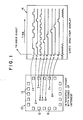
- Figure 1 is an illustration of an integrated circuit shown generally at 10 having a plurality of output pins 12 on the periphery thereof and a plurality of nodes 1-8 within the integrated circuit.
- the bit streams at each node during consecutive time periods must be determined, as illustrated by the timing diagram shown generally at 14.
- the logic state of each of the nodes 1-8 is mapped against the clock signal as illustrated.
- the timing diagram can be assembled by concatenating the logic levels of succeeding states at each of the nodes. The diagram will then yield information about the dynamic and logic operation of the circuit.
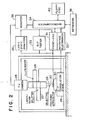
- FIG. 2 is a functional block diagram of a test system in accordance with the present invention.
- the device under test (DUT) 20 is provided on an X-Y translation table with an optics portion positioned generally thereabove.
- the optics portion includes a laser/ beam splitter 22, a TV camera 24 for viewing the DUT, and an illuminator 26.
- Each of the devices 22-26 is focused on the DUT by means of an objective lens 28.
- the TV camera allows the user to aim a laser spot on the node of interest.
- the light illuminator 26 illuminates the DUT field of interest for the TV camera, and the illuminator is turned off during the actual test.
- the laser/beam splitter injects the laser beam into the optics, and the objective lens focuses the laser beam and reduces the field of view for the camera.
- Focusing apparatus 30 allows the user to focus the surface of the DUT.
- Front end and data acquisition circuitry 31,32 operates under computer control and is triggered by the hardware logic state analyzer 35 . This circuitry extracts the current values at the proper states and sends the. values to the computer 34 for analysis. Computer 34 directs all activities of the other components to acquire, display, and store a generated timing diagram.
- the monitor 36 displays the image from TV camera 24 and the computer status, data, and output.
- a keyboard 38 allows the user to control and feed test parameters into the test system, and floppy discs 40 are provided for the permanent storage of timing diagrams and test vectors.
- FIG. 3 illustrates generally the correlated double sampling (CDS) method of obtaining data.
- the supply voltage, V DDJ is connected through a load 42 to the integrated circuit 20 device under test.
- Load 42 can be a resistor, as shown, or other suitable load means such as a current mirror, for example.
- a switch 43 bypasses resistor 42 except during the test procedure.
- the system clock 44 is allowed to run after a triggering event until a desired time period is reached, whereupon the clock is stopped and a transistor at a particular node under investigation within the integrated circuit 20 is then irradiated by a laser beam as illustrated. If the transistor is already conducting, the increase in load current will be much less than if the transistor is non-conducting before illumination.
- the change in node current is monitored by the double sampling technique in which the voltage at either end of the load resistor 42 is capactively coupled to the analog circuitry shown generally at 46.
- the analog circuitry includes several amplification stages which amplify the differential voltage impressed upon it during the desired time window when the clock 44 is stopped.
- the resulting amplified signal is then sent to an analog to digital converter, 48, and a digital signal is then transmitted through the control circuitry 50 to computer 52.
- the control circuitry 50 provides the clock signals ( ⁇ D , ⁇ A , ⁇ B , ⁇ C ,) for controlling the CDS circuitry 46 during the data acquisition, as will be described with reference to Figures 4 and 5.
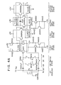
- FIG 4 is a detailed schematic of one embodiment of the CDS circuitry 46 of Figure 3.
- the circuitry provides capacitively coupled fully differential gain for a measured signal with temperature and dc drift insensitivity, and low noise.
- the circuitry includes a capacitive ac coupling stage, a switch stage for transient suppression and operating point reset, a first amplification stage, a first buffer, a second amplification stage, a second bipolar buffer, a second switch stage for eliminating charge injection noise and negation of drift and offset, a third amplification stage, a third bipolar buffer, and sample and hold circuitry followed by differential/single ended conversion of the amplified signal which is then connected to the A/D circuitry.
- FIG 5 illustrates the clock signals provided by the digital control circuitry 50 of Figure 3 in controlling data acquisition by the CDS circuitry.
- Either end of the load resistor or R L is capacitively coupled to the first gain stage which eliminates.the dc component of the integrated circuit supply current from the measurement. Independent biasing of the first gain stage is also permitted.
- the analog switches of the first switch stage perform the current transient suppression by isolating the sensitive analog circuits when the integrated circuit is operating and reset the gain stage operating point to ground. When the integrated circuit is operating, SWIA and SWIB are closed and SW2A is open. The gain section is therefore isolated and set to ground.
- SW1A and SW1B of the first switch stage opens while SW2A closes. This action disconnects the reference and connects the sense lines to the gain stage.
- the gain stage becomes active and amplifies sense line voltage changes. The particular arrangement cancels charge injection from switch transients.
- the minimum settling time for transient suppression is dominated by the RC time constant of the coupling capacitors and the SW1A switch on-resistance. By allowing six time constants for transient relaxation, the settling time before connection should then be greater than 900 nanoseconds.
- the first cain block consists of two gain stages and two buffer stages.
- the first amplifier stage is a high input impedance low-noise FET common-source stage.
- a bipolar buffer stage is placed between the FET first amplifier stage and the bipolar second amplifier stage.
- the overall block gain is about 455.
- the amplification of the bipolar gain section is purposely reduced with emitter shunting resistors to increase its bandwidth.
- the 20pF capacitor across the collectors lowers the 3dB frequency point for high frequency noise reduction.
- a bipolar second buffer stage performs an impedance conversion to isolate the bipolar second amplifier stage from the second gain block.
- Two 1800pF capacitors 60 and a SW3 B switch of the second switch stage perform an AC coupling/operating point reset.
- This circuitry eliminates prior device mismatches, offsets, and temperature drifts. It also eliminates the amplified charge injection noise of the first switch stage. The elimination is possible by firing JB some time after ⁇ A so that the error transients become DC voltage offsets across the capacitors 60. The transients will therefore not produce any differential signal in the second gain block.
- the second gain block consists of a FET common-source high impedance third amplifier stage, a bipolar third buffer for sample and hold capacitor drive capability, a sample/hold switch SW3A, sample and hold capacitors 62, and an instrumentation amplifier providing a differential/single ended conversion.
- the test apparatus Upon completion of a measurement, the test apparatus is reinitialised to the start of the test program and the clock is again started.
- the control computer 52 or digital control circuitry 50 issues parameters for a new measurement.
- One parameter is a binary number representing the number of clock cycles allowed to pass after the trigger even before again stopping the clock for the new measurement. Accordingly, any desired state for measurement is determined by setting a state counter. Since the measurement scheme arrives at the state of interest at the device clock rate, the logic level of the transistor at that state will reflect high speed operation of the device under test.
- a droop can occur in the current baseline which can shift the sampled voltages upwards or downwards.
- a cancellation of any droop can be effected by taking two successive state readings, one without laser irradiation and one with the irradiation. By subtracting the two readings, the droop is cancelled and the residual represents the true signal resulting from application of the laser.
- a test system employing the correlated double sampling in accordance with the invention allows a nearly constant AC baseline free of state .transition current transients. Because of the capacitively coupled fully differential detection scheme, the measurements are first order insensitive to power supply noise and to the integrated circuit current dissipation level. Only the relative data is measured thus the detection circuit does not require high dc and temperature stability.
Landscapes
- Physics & Mathematics (AREA)
- Engineering & Computer Science (AREA)
- Health & Medical Sciences (AREA)
- Computer Vision & Pattern Recognition (AREA)
- Electromagnetism (AREA)
- Toxicology (AREA)
- General Engineering & Computer Science (AREA)
- General Physics & Mathematics (AREA)
- Tests Of Electronic Circuits (AREA)
- Testing Or Measuring Of Semiconductors Or The Like (AREA)
- Testing Of Individual Semiconductor Devices (AREA)
- Semiconductor Integrated Circuits (AREA)
Priority Applications (1)
| Application Number | Priority Date | Filing Date | Title |
|---|---|---|---|
| AT84307853T ATE37097T1 (de) | 1983-11-15 | 1984-11-13 | System und verfahren zum testen fuer eine integrierte schaltung. |
Applications Claiming Priority (2)
| Application Number | Priority Date | Filing Date | Title |
|---|---|---|---|
| US06/552,089 US4588950A (en) | 1983-11-15 | 1983-11-15 | Test system for VLSI digital circuit and method of testing |
| US552089 | 1990-07-13 |
Publications (2)
| Publication Number | Publication Date |
|---|---|
| EP0142366A1 true EP0142366A1 (de) | 1985-05-22 |
| EP0142366B1 EP0142366B1 (de) | 1988-09-07 |
Family
ID=24203889
Family Applications (1)
| Application Number | Title | Priority Date | Filing Date |
|---|---|---|---|
| EP84307853A Expired EP0142366B1 (de) | 1983-11-15 | 1984-11-13 | System und Verfahren zum Testen für eine integrierte Schaltung |
Country Status (7)
| Country | Link |
|---|---|
| US (1) | US4588950A (de) |
| EP (1) | EP0142366B1 (de) |
| JP (1) | JPS60108768A (de) |
| KR (1) | KR850004352A (de) |
| AT (1) | ATE37097T1 (de) |
| CA (1) | CA1222329A (de) |
| DE (1) | DE3473930D1 (de) |
Cited By (3)
| Publication number | Priority date | Publication date | Assignee | Title |
|---|---|---|---|---|
| GB2185327A (en) * | 1986-01-13 | 1987-07-15 | Robert Howard Jones | A method of testing an electrical chip |
| EP0483983A3 (en) * | 1990-10-29 | 1992-09-23 | Hewlett-Packard Company | Method and apparatus for the detection of leakage current |
| DE19908186C2 (de) * | 1999-02-25 | 2001-08-09 | Infineon Technologies Ag | Integrierte Schaltkreis, Verfahren zu seiner Herstellung, Gußform zur Durchführung des Verfahrens und Verfahren zur Funktionsprüfung des integrierten Schaltkreises |
Families Citing this family (68)
| Publication number | Priority date | Publication date | Assignee | Title |
|---|---|---|---|---|
| US4698587A (en) * | 1985-03-28 | 1987-10-06 | The United States Of America As Represented By The Secretary Of The Air Force | Method of characterizing critical timing paths and analyzing timing related failure modes in very large scale integrated circuits |
| US4786864A (en) * | 1985-03-29 | 1988-11-22 | International Business Machines Corporation | Photon assisted tunneling testing of passivated integrated circuits |
| US4755748A (en) * | 1985-06-05 | 1988-07-05 | Bell Communications Research, Inc. | Method and apparatus for analyzing semiconductor devices using charge-sensitive electron-beam-injected-carrier microscopy |
| JPS622552A (ja) * | 1985-06-27 | 1987-01-08 | Matsushita Electric Ind Co Ltd | 半導体検査装置および半導体検査方法 |
| US4703260A (en) * | 1985-09-23 | 1987-10-27 | International Business Machines Corporation | Full chip integrated circuit tester |
| US4704550A (en) * | 1986-11-07 | 1987-11-03 | American Telephone And Telegraph Company | Method and apparatus for driving electrical circuits |
| NL8700933A (nl) * | 1987-04-21 | 1988-11-16 | Philips Nv | Testmethode voor lcd-elementen. |
| DE3889986T2 (de) * | 1987-07-13 | 1994-09-15 | Hamamatsu Photonics Kk | Anordnung eines Spannungsdetektors. |
| US4845475A (en) * | 1987-11-17 | 1989-07-04 | The Boeing Company | Automatic testing of position sensing devices employing stored sensed position |
| DD273695A1 (de) * | 1988-07-04 | 1989-11-22 | Univ Schiller Jena | Verfahren zur erfassung schnell ablaufender prozesse in integrierten schaltkreisen unter verwendung eines laser-raster-mikroskopes mit obic-stufe |
| FR2656932B1 (fr) * | 1990-01-09 | 1992-05-07 | Sgs Thomson Microelectronics | Circuit de mesure du courant dans un transistor mos de puissance. |
| US5208531A (en) * | 1990-08-13 | 1993-05-04 | Texas Instruments Incorporated | Apparatus and method for testing integrated circuits |
| JPH05136240A (ja) * | 1991-11-14 | 1993-06-01 | Mitsubishi Electric Corp | Obic観察方法およびその装置 |
| US5334540A (en) * | 1991-11-14 | 1994-08-02 | Mitsubishi Denki Kabushiki Kaisha | OBIC observation method and apparatus therefor |
| US5345170A (en) | 1992-06-11 | 1994-09-06 | Cascade Microtech, Inc. | Wafer probe station having integrated guarding, Kelvin connection and shielding systems |
| US6380751B2 (en) | 1992-06-11 | 2002-04-30 | Cascade Microtech, Inc. | Wafer probe station having environment control enclosure |
| US5659244A (en) * | 1994-09-21 | 1997-08-19 | Nec Corporation | Electronic circuit tester and method of testing electronic circuit |
| US6232789B1 (en) | 1997-05-28 | 2001-05-15 | Cascade Microtech, Inc. | Probe holder for low current measurements |
| US5561377A (en) | 1995-04-14 | 1996-10-01 | Cascade Microtech, Inc. | System for evaluating probing networks |
| US5914613A (en) | 1996-08-08 | 1999-06-22 | Cascade Microtech, Inc. | Membrane probing system with local contact scrub |
| US6169408B1 (en) | 1996-09-30 | 2001-01-02 | Motorola, Inc. | Method and apparatus for testing an integrated circuit with a pulsed radiation beam |
| US6002263A (en) | 1997-06-06 | 1999-12-14 | Cascade Microtech, Inc. | Probe station having inner and outer shielding |
| US6421085B1 (en) | 1998-04-14 | 2002-07-16 | Eastman Kodak Company | High speed CMOS imager column CDS circuit |
| US6256882B1 (en) | 1998-07-14 | 2001-07-10 | Cascade Microtech, Inc. | Membrane probing system |
| US6578264B1 (en) | 1999-06-04 | 2003-06-17 | Cascade Microtech, Inc. | Method for constructing a membrane probe using a depression |
| US6445202B1 (en) | 1999-06-30 | 2002-09-03 | Cascade Microtech, Inc. | Probe station thermal chuck with shielding for capacitive current |
| US6838890B2 (en) | 2000-02-25 | 2005-01-04 | Cascade Microtech, Inc. | Membrane probing system |
| US6965226B2 (en) | 2000-09-05 | 2005-11-15 | Cascade Microtech, Inc. | Chuck for holding a device under test |
| US6914423B2 (en) | 2000-09-05 | 2005-07-05 | Cascade Microtech, Inc. | Probe station |
| DE10143173A1 (de) | 2000-12-04 | 2002-06-06 | Cascade Microtech Inc | Wafersonde |
| WO2003052435A1 (en) | 2001-08-21 | 2003-06-26 | Cascade Microtech, Inc. | Membrane probing system |
| US6777964B2 (en) | 2002-01-25 | 2004-08-17 | Cascade Microtech, Inc. | Probe station |
| JP2005527823A (ja) | 2002-05-23 | 2005-09-15 | カスケード マイクロテック インコーポレイテッド | デバイスのテスト用プローブ |
| DE10239638A1 (de) * | 2002-08-29 | 2004-03-25 | Krones Ag | Verfahren, Vorrichtung und System zum Anzeigen von Daten eines Maschinensteuerung-Systems |
| US6847219B1 (en) | 2002-11-08 | 2005-01-25 | Cascade Microtech, Inc. | Probe station with low noise characteristics |
| US6724205B1 (en) | 2002-11-13 | 2004-04-20 | Cascade Microtech, Inc. | Probe for combined signals |
| US7250779B2 (en) | 2002-11-25 | 2007-07-31 | Cascade Microtech, Inc. | Probe station with low inductance path |
| US6861856B2 (en) | 2002-12-13 | 2005-03-01 | Cascade Microtech, Inc. | Guarded tub enclosure |
| US7221172B2 (en) | 2003-05-06 | 2007-05-22 | Cascade Microtech, Inc. | Switched suspended conductor and connection |
| US7057404B2 (en) | 2003-05-23 | 2006-06-06 | Sharp Laboratories Of America, Inc. | Shielded probe for testing a device under test |
| US7492172B2 (en) | 2003-05-23 | 2009-02-17 | Cascade Microtech, Inc. | Chuck for holding a device under test |
| US7250626B2 (en) | 2003-10-22 | 2007-07-31 | Cascade Microtech, Inc. | Probe testing structure |
| DE202004021093U1 (de) | 2003-12-24 | 2006-09-28 | Cascade Microtech, Inc., Beaverton | Aktiver Halbleiterscheibenmessfühler |
| US7187188B2 (en) | 2003-12-24 | 2007-03-06 | Cascade Microtech, Inc. | Chuck with integrated wafer support |
| JP2008502167A (ja) | 2004-06-07 | 2008-01-24 | カスケード マイクロテック インコーポレイテッド | 熱光学チャック |
| US7330041B2 (en) | 2004-06-14 | 2008-02-12 | Cascade Microtech, Inc. | Localizing a temperature of a device for testing |
| US7368927B2 (en) | 2004-07-07 | 2008-05-06 | Cascade Microtech, Inc. | Probe head having a membrane suspended probe |
| KR20070058522A (ko) | 2004-09-13 | 2007-06-08 | 캐스케이드 마이크로테크 인코포레이티드 | 양측 프루빙 구조 |
| US7535247B2 (en) | 2005-01-31 | 2009-05-19 | Cascade Microtech, Inc. | Interface for testing semiconductors |
| US7656172B2 (en) | 2005-01-31 | 2010-02-02 | Cascade Microtech, Inc. | System for testing semiconductors |
| US7449899B2 (en) | 2005-06-08 | 2008-11-11 | Cascade Microtech, Inc. | Probe for high frequency signals |
| JP5080459B2 (ja) | 2005-06-13 | 2012-11-21 | カスケード マイクロテック インコーポレイテッド | 広帯域能動/受動差動信号プローブ |
| US7659981B2 (en) * | 2005-08-26 | 2010-02-09 | Dcg Systems, Inc. | Apparatus and method for probing integrated circuits using polarization difference probing |
| US7450245B2 (en) | 2005-06-29 | 2008-11-11 | Dcg Systems, Inc. | Method and apparatus for measuring high-bandwidth electrical signals using modulation in an optical probing system |
| US7733100B2 (en) | 2005-08-26 | 2010-06-08 | Dcg Systems, Inc. | System and method for modulation mapping |
| DE202007018733U1 (de) | 2006-06-09 | 2009-03-26 | Cascade Microtech, Inc., Beaverton | Messfühler für differentielle Signale mit integrierter Symmetrieschaltung |
| US7723999B2 (en) | 2006-06-12 | 2010-05-25 | Cascade Microtech, Inc. | Calibration structures for differential signal probing |
| US7764072B2 (en) | 2006-06-12 | 2010-07-27 | Cascade Microtech, Inc. | Differential signal probing system |
| US7443186B2 (en) | 2006-06-12 | 2008-10-28 | Cascade Microtech, Inc. | On-wafer test structures for differential signals |
| US7403028B2 (en) | 2006-06-12 | 2008-07-22 | Cascade Microtech, Inc. | Test structure and probe for differential signals |
| US7876114B2 (en) | 2007-08-08 | 2011-01-25 | Cascade Microtech, Inc. | Differential waveguide probe |
| US20090147255A1 (en) * | 2007-12-07 | 2009-06-11 | Erington Kent B | Method for testing a semiconductor device and a semiconductor device testing system |
| US7888957B2 (en) | 2008-10-06 | 2011-02-15 | Cascade Microtech, Inc. | Probing apparatus with impedance optimized interface |
| WO2010059247A2 (en) | 2008-11-21 | 2010-05-27 | Cascade Microtech, Inc. | Replaceable coupon for a probing apparatus |
| US8319503B2 (en) | 2008-11-24 | 2012-11-27 | Cascade Microtech, Inc. | Test apparatus for measuring a characteristic of a device under test |
| SG10201401887YA (en) | 2009-05-01 | 2014-06-27 | Dcg Systems Inc | Systems and method for laser voltage imaging state mapping |
| JP6611387B1 (ja) * | 2018-08-30 | 2019-11-27 | 浜松ホトニクス株式会社 | 半導体試料の検査装置及び検査方法 |
| KR20250168455A (ko) | 2023-03-31 | 2025-12-02 | 하마마츠 포토닉스 가부시키가이샤 | 검사 장치 및 검사 방법 |
Family Cites Families (3)
| Publication number | Priority date | Publication date | Assignee | Title |
|---|---|---|---|---|
| US4242635A (en) * | 1979-01-26 | 1980-12-30 | The United States Of America As Represented By The Secretary Of The Air Force | Apparatus and method for integrated circuit test analysis |
| US4287441A (en) * | 1979-03-30 | 1981-09-01 | The United States Of America As Represented By The Secretary Of The Army | Correlated double sampling CCD video preprocessor-amplifier |
| JPS5876910A (ja) * | 1981-10-30 | 1983-05-10 | Konishiroku Photo Ind Co Ltd | 異常検出装置 |
-
1983
- 1983-11-15 US US06/552,089 patent/US4588950A/en not_active Expired - Fee Related
-
1984
- 1984-10-02 JP JP59206975A patent/JPS60108768A/ja active Pending
- 1984-11-13 DE DE8484307853T patent/DE3473930D1/de not_active Expired
- 1984-11-13 EP EP84307853A patent/EP0142366B1/de not_active Expired
- 1984-11-13 AT AT84307853T patent/ATE37097T1/de not_active IP Right Cessation
- 1984-11-14 CA CA000467825A patent/CA1222329A/en not_active Expired
- 1984-11-15 KR KR1019840007158A patent/KR850004352A/ko not_active Withdrawn
Non-Patent Citations (3)
| Title |
|---|
| ELECTRONICS, vol. 44, no. 8, 12th April 1971, pages 92-95, New York, US; R.E. McMAHON: "Laser tests ICs with light touch" * |
| MICROELECTRONICS & RELIABILITY, vol. 20, no. 5, 1980, pages 717-735, Pergamon Press Ltd., Oxford, GB; M. NAGASE: "A device analysis system based on laser scanning techniques" * |
| PROCEEDINGS OF THE INSTITUTE OF ELECTRICAL AND ELECTRONIC ENGINEERS; vol. 64, no. 3, 1976, pages 393-394, New York, US; D.E. SAWYER et al.: "Laser scanning of MOS IC's reveals internal logic states nondestructively" * |
Cited By (4)
| Publication number | Priority date | Publication date | Assignee | Title |
|---|---|---|---|---|
| GB2185327A (en) * | 1986-01-13 | 1987-07-15 | Robert Howard Jones | A method of testing an electrical chip |
| GB2185327B (en) * | 1986-01-13 | 1990-05-30 | Robert Howard Jones | A method of testing an electrical chip |
| EP0483983A3 (en) * | 1990-10-29 | 1992-09-23 | Hewlett-Packard Company | Method and apparatus for the detection of leakage current |
| DE19908186C2 (de) * | 1999-02-25 | 2001-08-09 | Infineon Technologies Ag | Integrierte Schaltkreis, Verfahren zu seiner Herstellung, Gußform zur Durchführung des Verfahrens und Verfahren zur Funktionsprüfung des integrierten Schaltkreises |
Also Published As
| Publication number | Publication date |
|---|---|
| JPS60108768A (ja) | 1985-06-14 |
| CA1222329A (en) | 1987-05-26 |
| ATE37097T1 (de) | 1988-09-15 |
| EP0142366B1 (de) | 1988-09-07 |
| KR850004352A (ko) | 1985-07-11 |
| US4588950A (en) | 1986-05-13 |
| DE3473930D1 (en) | 1988-10-13 |
Similar Documents
| Publication | Publication Date | Title |
|---|---|---|
| EP0142366B1 (de) | System und Verfahren zum Testen für eine integrierte Schaltung | |
| US4714875A (en) | Printed circuit board fault location system | |
| US5789933A (en) | Method and apparatus for determining IDDQ | |
| US5483170A (en) | Integrated circuit fault testing implementing voltage supply rail pulsing and corresponding instantaneous current response analysis | |
| US20230408577A1 (en) | Low current leakage measurement on a high current unified static and dynamic characterization platform | |
| US6169408B1 (en) | Method and apparatus for testing an integrated circuit with a pulsed radiation beam | |
| US4694242A (en) | Integrated circuit tester and remote pin electronics therefor | |
| US5905381A (en) | Functional OBIC analysis | |
| US5101152A (en) | Integrated circuit transfer test device system utilizing lateral transistors | |
| US6714036B2 (en) | Monitor circuitry and method for testing analog and/or mixed signal integrated circuits | |
| US3869666A (en) | Maximum slope detectors | |
| US6759864B2 (en) | System and method for testing integrated circuits by transient signal analysis | |
| EP0436358B1 (de) | Integrierte Schaltung mit einem die Unversehrtheit eines Energiequellenanschlusses überprüfenden Monitors | |
| JPH03138570A (ja) | 過渡電流ピーク検出回路 | |
| US4506212A (en) | Method and apparatus for testing integrated circuits using AC test input and comparison of resulting frequency spectrum outputs | |
| JP3000746B2 (ja) | 半導体装置の特性測定方法 | |
| Maidon et al. | Using IDD to analyze analog faults and development of a sensor | |
| JP2596041Y2 (ja) | Icテスタ | |
| JP2827233B2 (ja) | 半導体試験装置 | |
| JP3214192B2 (ja) | Icテスタ | |
| KR940006602B1 (ko) | 포탄 근접 신관의 하이브리드 회로(hybrid IC) 측정장치 | |
| JP2648947B2 (ja) | 半導体装置の検査装置 | |
| Mandl et al. | High-throughput testing and characterization of IR readouts and hybrids | |
| JPH07174814A (ja) | 素子試験方法 | |
| JPS6126630B2 (de) |
Legal Events
| Date | Code | Title | Description |
|---|---|---|---|
| PUAI | Public reference made under article 153(3) epc to a published international application that has entered the european phase |
Free format text: ORIGINAL CODE: 0009012 |
|
| AK | Designated contracting states |
Designated state(s): AT CH DE FR GB IT LI NL SE |
|
| 17P | Request for examination filed |
Effective date: 19851115 |
|
| 17Q | First examination report despatched |
Effective date: 19870113 |
|
| GRAA | (expected) grant |
Free format text: ORIGINAL CODE: 0009210 |
|
| AK | Designated contracting states |
Kind code of ref document: B1 Designated state(s): AT CH DE FR GB IT LI NL SE |
|
| PG25 | Lapsed in a contracting state [announced via postgrant information from national office to epo] |
Ref country code: SE Effective date: 19880907 Ref country code: NL Effective date: 19880907 Ref country code: LI Effective date: 19880907 Ref country code: IT Free format text: LAPSE BECAUSE OF FAILURE TO SUBMIT A TRANSLATION OF THE DESCRIPTION OR TO PAY THE FEE WITHIN THE PRESCRIBED TIME-LIMIT;WARNING: LAPSES OF ITALIAN PATENTS WITH EFFECTIVE DATE BEFORE 2007 MAY HAVE OCCURRED AT ANY TIME BEFORE 2007. THE CORRECT EFFECTIVE DATE MAY BE DIFFERENT FROM THE ONE RECORDED. Effective date: 19880907 Ref country code: CH Effective date: 19880907 Ref country code: AT Effective date: 19880907 |
|
| REF | Corresponds to: |
Ref document number: 37097 Country of ref document: AT Date of ref document: 19880915 Kind code of ref document: T |
|
| REF | Corresponds to: |
Ref document number: 3473930 Country of ref document: DE Date of ref document: 19881013 |
|
| ET | Fr: translation filed | ||
| REG | Reference to a national code |
Ref country code: CH Ref legal event code: PL |
|
| PGFP | Annual fee paid to national office [announced via postgrant information from national office to epo] |
Ref country code: DE Payment date: 19881230 Year of fee payment: 5 |
|
| NLV1 | Nl: lapsed or annulled due to failure to fulfill the requirements of art. 29p and 29m of the patents act | ||
| PLBE | No opposition filed within time limit |
Free format text: ORIGINAL CODE: 0009261 |
|
| STAA | Information on the status of an ep patent application or granted ep patent |
Free format text: STATUS: NO OPPOSITION FILED WITHIN TIME LIMIT |
|
| 26N | No opposition filed | ||
| PG25 | Lapsed in a contracting state [announced via postgrant information from national office to epo] |
Ref country code: GB Effective date: 19891113 |
|
| GBPC | Gb: european patent ceased through non-payment of renewal fee | ||
| PG25 | Lapsed in a contracting state [announced via postgrant information from national office to epo] |
Ref country code: FR Effective date: 19900731 |
|
| PG25 | Lapsed in a contracting state [announced via postgrant information from national office to epo] |
Ref country code: DE Effective date: 19900801 |
|
| REG | Reference to a national code |
Ref country code: FR Ref legal event code: ST |