EP0143553A1 - Procédé et dispositif pour la conversion de données digitales - Google Patents
Procédé et dispositif pour la conversion de données digitales Download PDFInfo
- Publication number
- EP0143553A1 EP0143553A1 EP84307387A EP84307387A EP0143553A1 EP 0143553 A1 EP0143553 A1 EP 0143553A1 EP 84307387 A EP84307387 A EP 84307387A EP 84307387 A EP84307387 A EP 84307387A EP 0143553 A1 EP0143553 A1 EP 0143553A1
- Authority
- EP
- European Patent Office
- Prior art keywords
- converted
- bit
- digital signal
- bits
- words
- Prior art date
- Legal status (The legal status is an assumption and is not a legal conclusion. Google has not performed a legal analysis and makes no representation as to the accuracy of the status listed.)
- Granted
Links
Images




Classifications
-
- G—PHYSICS
- G11—INFORMATION STORAGE
- G11B—INFORMATION STORAGE BASED ON RELATIVE MOVEMENT BETWEEN RECORD CARRIER AND TRANSDUCER
- G11B20/00—Signal processing not specific to the method of recording or reproducing; Circuits therefor
- G11B20/10—Digital recording or reproducing
- G11B20/14—Digital recording or reproducing using self-clocking codes
- G11B20/1403—Digital recording or reproducing using self-clocking codes characterised by the use of two levels
- G11B20/1423—Code representation depending on subsequent bits, e.g. delay modulation, double density code, Miller code
- G11B20/1426—Code representation depending on subsequent bits, e.g. delay modulation, double density code, Miller code conversion to or from block codes or representations thereof
Definitions
- This invention relates to methods of and apparatus for digital data conversion and, more particularly, but not exclusively, to such methods and apparatus suitable for use where a digital signal is to be transmitted or recorded.
- an analog audio signal can be recorded and reproduced with high fidelity by converting the analog audio signal into a pulse code modulated (PCM) audio signal which is magnetically recorded without guard bands using a rotary head, and is then reproduced and reconverted to analog form.
- PCM pulse code modulated
- low frequency components tend to be cut off by a rotary transformer associated with the rotary head, so that there is some loss of fidelity in the low frequency region.
- NRZI non-return to zero, inverted
- the modulated signal when consecutive digital zeroes appear, the modulated signal is not inverted during that period, and the frequency thereof becomes low, so the defect occurs that the DC component and the low frequency component are increased.
- This system employs an 8/10 converting scheme in which each eight bits of digital information in a basic digital signal are converted to a 10-bit word to form a converted digital signal.
- Eight bits (B 1 , B 2 , B 3 , B 4 , B 5 , B 61 B 7 , Bg) can have 256 (2 ) combinations. With ten bits, 1024 (2 ) combinations are possible. Thus, 256 of the 1024 possible 10-bit combinations are used to represent the 8-bit combinations.
- Table I shows the possible combinations of ten digital bits in NRZI code for which the DC component is zero, but in which there are no more than three consecutive digital zeroes (either internally of each 10-bit word or at the junction between two such words):
- Table I shows that there are numerous possible combinations that will satisfy the constraints. For example, if up to three digital zeroes are permitted at the beginning of each word, then no digital zeroes can be permitted at the end of any word. In that case, Table I shows that the total of the possible combinations is:
- the maximum total is achieved if no more than two digital zeroes are permitted at the beginning of a 10-bit converted word and no more than one digital zero is permitted at the end. In that case, the total is:
- Table n illustrates the number of possible combinations of 10-bit combinations, which begin with no more than two digital zeroes and end with no more than one digital zero, having a DC component of zero, -2 or +2 when NRZI-coded.
- the low frequency spectrum of the modulation wave tends to be less if combinations alternately using combinations with DC components +2 and -2 are used more frequently than the combinations with a DC component of zero. Accordingly, the 125 combinations with a pair of +2 and -2 DC components are used, and for the remaining 131 combinations those with a DC component of zero are used to give a total of 256 combinations corresponding respectively to the 256 possible combinations of eight bits.
- the pairs may be selected such that the DC component can be controlled merely by changing the first bit (the second bit and the following bits in the combinations of a pair having the same level). Therefore, of the possible combinations in, for example, Table II, the combinations with DC components of +2 and -2 and the first bit "0" total:
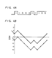
- the DC component of each bit is referred to as the digital sum variation (DSV) in some evaluation methods.
- DSV digital sum variation
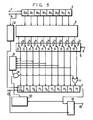
- FIG. 5 of the accompanying drawings shows an example of an apparatus which is capable of conversion in accordance with the above converting system.
- the apparatus comprises an input terminal 1, an 8-bit shift register 2 which accepts information of eight bits, a conversion logic circuit 3 which uses, for example, a programmable logic array (PLA), and a clock terminal 4.
- the information supplied to the input terminal 1 is transferred eight bits at a time through the shift register 2 in response to a pulse which is supplied to the clock terminal 4 at the data bit rate, and the information of eight bits (B 1 , B 2 , B 3 , B 4 , B 5 , B 6 , B 7 , 8 8 ) is supplied to the conversion logic circuit 3.
- PDA programmable logic array
- a data sync (synchronizing) pattern selecting circuit 5 is controlled in selection operation on the basis of a data/sync selection control signal supplied to a terminal 6.
- a data/sync selection control signal supplied to a terminal 6.
- a detecting circuit 8 detects whether the first bit is variable or fixed, namely, whether the combination has a DC component of zero or +2. For example, the detecting circuit 8 carries out modulo-addition for even-numbered bits of the outputs of the selecting circuit 5, or detects whether the number of digital zeroes of the even-numbered bits is even or odd. When the number is zero (even), the detecting circuit 8 detects or judges that the combination has a DC component of ⁇ 2, so that the detecting circuit 8 produces at its output side a high level or digital "1".
- the output of the detecting circuit 8 is supplied to one input terminal of an AND circuit 9, and the AND circuit 9 is supplied at the other input terminal with an output from a detecting circuit 10 which is provided at the output side of the shift register 7 for detecting DC charge (DSV) of each combination.
- the detecting circuit 10 supplies the high level output to the input side of the AND circuit 9 when the DSV up to the preceding combination is, for example, -1.
- the output of the AND circuit 9 is supplied to one input terminal of an exclusive-OR (ex-OR) circuit 11 which inverts the first bit in level.
- an exclusive-OR (ex-OR) circuit 11 which inverts the first bit in level.
- a first bit P i of ten bits from the selecting circuit 5. Accordingly, when the output of the AND circuit 9 is "0", the first bit P 1 is not inverted in level and is fed to the shift register 7, while when the output of the AND circuit 9 is "1", the first bit P l is inverted in polarity and is fed to the shift register 7.
- the conversion logic circuit 3 when the conversion logic circuit 3 produces an output with a DC component of -2, if the converted combination has a DC component of -2 and the evaluation of DSV variance begins with -1, the first bit thereof is inverted in level by the ex-OR circuit 11 (at this time, the output of the AND circuit 9 is at high level) and it is produced as a combination having a DC component +2. Since the output of the detecting circuit 8 is at low level and the output of the AND circuit 9 is at low level for the combination with a DC component of zero, it is directly produced without its first bit being inverted in level by the ex-OR circuit 11.
- a timing detection circuit 12 detects the timing of the pulse which is supplied to the clock terminal 1 at the data bit rate, and the timing signal from the timing detection circuit 12 is supplied to a load terminal LD of the shift register 7 at every eight bits of data.
- the data converted to the form of 10-bit data and latched in the shift register 7 are sequentially read out therefrom on the basis of a clock signal with frequency 5/4 times the clock frequency of the input signal and supplied thereto from a clock terminal 13.
- the signal thus read out is supplied to, for example, a T type flip-flop circuit 14 serving as an NRZI-coding circuit, and on the basis of the clock signal supplied from the clock terminal 13 to the clock terminal of the flip-flop circuit 14, the flip-flop circuit 14 produces at an output terminal 15 a signal which has been NRZI-coded.
- FIG. 6 of the accompanying drawings schematically shows an example of an apparatus for demodulating the information which has been modulated in accordance with the above method.
- a signal is supplied via an inlet terminal 21 through an NRZI demodulating circuit 22 to a 10-bit shift register 23.
- Information of ten bits is transferred throughout the 10-bit shift register 23 on the basis of a pulse signal of the code bit rate supplied thereto from a clock terminal 24.
- Information of ten bits, P i to P 10 from the shift register 23 is supplied to a conversion logic circuit 25 which uses, for example, a PLA (programmable logic array).
- a detecting circuit 26 which detects the DSV of each combination, and the output of the detecting circuit 26 is supplied to one input terminal of an ex-OR circuit 27. To the other input terminal of the ex-OR circuit 27 is supplied the first bit P I of the output from the shift register 23.
- the input to the conversion logic circuit 25 is unified as either a combination with a DC component of zero or a combination with a DC component of +2.
- the detecting circuit 26 produces the high level output when the DSV up to the preceding combination is -1.
- the ex-OR circuit 27 when supplied with a combination with a DC component of +2 from the shift register 23, the ex-OR circuit 27 inverts its first bit in level and produces the same, while when supplied with a combination with a DC component of -2 from the shift register 23, the ex-OR circuit 27 produces the first bit as it is.
- the information of ten bits, P 1 to P10 is demodulated using one-to-one reverse conversion. Accordingly, the demodulated information of eight bits, B 1 to B 8 , is supplied to an 8-bit shift register 28 and latched therein by a pulse supplied thereto from a clock terminal 29 each time a timing signal (a pulse of each block) which results from detecting by a timing detection circuit 30 is supplied to a load terminal LD of the shift register 28. Then, the data in the shift register 28 are shifted bit by bit on the basis of a pulse which is supplied to its clock terminal at a data bit rate and developed at an output terminal 31.
- the circuit for detecting whether the combination has a DC component of zero or +2 is required, so the circuit arrangement becomes complicated.
- ROM read-only memory
- the ROM causes the circuit arrangement to become large, and when this ROM is formed as an integrated circuit (IC), the ROM occupies a large pattern area and consumes much power.
- a method of deriving a digital signal having at least two signal levels, a DC component substantially equal to zero, and a predetermined maximum time between level transitions comprising the steps of:
- a converted digital signal is provided in an NRZI code with a DC component of zero and with a maximum predetermined number of bits between level transitions in the signal.
- the basic digital signal is divided into m-bit basic words, each of which is then converted into an n-bit converted code to form a converted digital signal suitable for recording.
- the n-bit converted code includes a plurality of primary combinations having a DC component substantially equal to zero when NRZI-coded, and a plurality of secondary combinations having a DC component with an absolute value of two when NRZI-coded.
- a variance of the DC component of the primary combination when NRZI-coded and the polarity of the DC component of the secondary combination when NRZI-coded are altered in response to the DC component of the preceding converted digital signal.
- a converting apparatus for deriving a digital signal having at least two signal levels, a DC component substantially equal to zero, and a predetermined maximum time between level changes, the apparatus comprising:
- 8-bit data is converted to 10-bit data.
- the first bit thereof is converted similarly to the combination in which the DC component is +2.
- Tmax 5T
- the number of consecutive digital zeroes must never exceed four, or the same consecutive levels of digital signal after being modulated must never exceed five bits. Therefore, the bits must begin with at most two digital zeroes and also end with at most two digital zeroes.
- Table III shows 102 possible combinations (hereinafter referred to as the primary combinations) each of which forms a pair having a DC component of zero and with a different first bit, and 154 possible combinations (hereinafter referred to as the secondary combinations) each of which forms a pair having a DC component of +2 with a different first bit.
- Table IV shows examples of 256 possible combinations (codes) which are selected on the basis of Table III, in which they are not corresponded to the data. Table IV shows that a pair of two combinations should be selected only by controlling, for example, the first bit.
- reference Q designates the DC component information (corresponding to the preceding DSV) of the code (combination) before being converted
- DV designates the variance of DSV
- P designates the number of level transitions (even number is 0 and odd number is 1) in each code
- Q designates the DC charge information (corresponding to the DSV of the code after just being converted) of the code just after being converted.
- Table VI shows examples of 278 different combinations (codes) selected on the basis of Table V. These combinations are not made corresponding to data. In Table VI, a pair of combinations are selected only by controlling the level of the first bit, similarly to Table IV. In Table VI, references such as Q are used for the same purpose as in Table VI.
- Figure 8 illustrates an example of an apparatus for carrying out the conversion in accordance with the conversion method of this invention.
- like parts corresponding to those in Figure 5 have the same references and will not be described in detail.
- the conversion apparatus of Figure 8 does not require a detecting circuit to detect whether the first bit is variable or fixed, namely, the detecting or controlling circuit 8 for controlling the combination with a DC component of zero (the first bit is fixed) and the combination with a DC component of +2 DC (the first bit is variable) as shown in Figure 5 and so on.
- the output of the detecting circuit 10 for detecting the DC component (DSV) is directly supplied to one input terminal of the ex-OR circuit 11.
- the other circuit arrangements are the same as those in Figure 5.
- the content of the shift register 7 is read out on the basis of the clock signal supplied thereto from the clock terminal 13, fed to the flip-flop circuit 14, and then developed at the output terminal 15 as the NRZI-coded signal.
- Figure 9 illustrates an example of a demodulation apparatus.
- like parts corresponding to those in Figure 6 have the same references and will not be described in detail.
- this variable first bit is merely used to enhance the DC property and is not directly related to the data words, so that the nine bits other than the first bit are supplied from the shift register 23 to a conversion logic circuit 25. Accordingly, in this case, this conversion logic circuit 25 is not of the 10/8- conversion tye but may be of a 9/8-conversion type, so the circuit arrangement is simplified. In association therewith, the detecting circuit 26 and the ex-OR circuit 27 used in Figure 6 become unnecessary.
- FIGs 10A and 10B and Figures 11A and 11B respectively illustrate an example of a sync pattern used in this embodiment.
- This sync pattern is a combination which cannot be realised in the ordinary conversion, so as to detect the groups of ten bits at the time of demodulation.
Landscapes
- Engineering & Computer Science (AREA)
- Signal Processing (AREA)
- Signal Processing For Digital Recording And Reproducing (AREA)
- Dc Digital Transmission (AREA)
- Compression, Expansion, Code Conversion, And Decoders (AREA)
Applications Claiming Priority (2)
| Application Number | Priority Date | Filing Date | Title |
|---|---|---|---|
| JP201587/83 | 1983-10-27 | ||
| JP58201587A JPH0683271B2 (ja) | 1983-10-27 | 1983-10-27 | 情報変換方式 |
Publications (2)
| Publication Number | Publication Date |
|---|---|
| EP0143553A1 true EP0143553A1 (fr) | 1985-06-05 |
| EP0143553B1 EP0143553B1 (fr) | 1989-01-04 |
Family
ID=16443524
Family Applications (1)
| Application Number | Title | Priority Date | Filing Date |
|---|---|---|---|
| EP84307387A Expired EP0143553B1 (fr) | 1983-10-27 | 1984-10-26 | Procédé et dispositif pour la conversion de données digitales |
Country Status (5)
| Country | Link |
|---|---|
| US (1) | US4626826A (fr) |
| EP (1) | EP0143553B1 (fr) |
| JP (1) | JPH0683271B2 (fr) |
| CA (1) | CA1244950A (fr) |
| DE (1) | DE3475978D1 (fr) |
Cited By (8)
| Publication number | Priority date | Publication date | Assignee | Title |
|---|---|---|---|---|
| EP0240146A3 (en) * | 1986-03-26 | 1990-06-20 | Northern Telecom Limited | Method and apparatus for the channelized serial transmission of redundantly encoded binary data |
| EP0310041A3 (fr) * | 1987-09-28 | 1990-08-22 | Nec Home Electronics, Ltd. | Système de conversion de code 8 bit à 9 bit et 8/9 convertisseur |
| EP0143005B1 (fr) * | 1983-11-24 | 1990-11-07 | Sony Corporation | Méthode et appareil pour convertir des données numériques |
| GB2232858A (en) * | 1989-05-31 | 1990-12-19 | Int Computers Ltd | Data transmission code |
| EP0537407A1 (fr) * | 1991-10-14 | 1993-04-21 | International Business Machines Corporation | Méthode de codage flexible et architecture pour transmission et enregistrement de données à haute vitesse |
| EP0472375A3 (en) * | 1990-08-18 | 1993-10-27 | Mitsubishi Electric Corp | Data conversion method, pilot signal formation method using the same and rotary magnetic head device using the same |
| EP0602966A3 (fr) * | 1992-12-16 | 1995-02-15 | Canon Kk | Appareil d'enregistrement et/ou de reproduction d'information d'information. |
| RU2171505C2 (ru) * | 1994-07-08 | 2001-07-27 | Сони Корпорейшн | Способы и устройства модулирования и демодулирования сигналов |
Families Citing this family (25)
| Publication number | Priority date | Publication date | Assignee | Title |
|---|---|---|---|---|
| JPS6231069A (ja) * | 1985-04-26 | 1987-02-10 | Mitsubishi Electric Corp | 記録媒体 |
| FR2589653B1 (fr) * | 1985-11-05 | 1990-03-23 | Lignes Telegraph Telephon | Dispositif de mise en oeuvre d'un code a faible disparite accumulee en transmission numerique a haut debit et procede de codage utilisant un tel dispositif |
| BE904913A (nl) * | 1986-06-13 | 1986-12-15 | Bell Telephone Mfg | Data overdrachtsysteem. |
| US4864303A (en) * | 1987-02-13 | 1989-09-05 | Board Of Trustees Of The University Of Illinois | Encoder/decoder system and methodology utilizing conservative coding with block delimiters, for serial communication |
| US4775985A (en) * | 1987-04-06 | 1988-10-04 | Sony Corporation | Method of dc-free 8/9 nrz coding using a unique sync word pattern |
| JP2974678B2 (ja) * | 1988-06-23 | 1999-11-10 | ソニー株式会社 | データ誤り検出方式 |
| JP2870843B2 (ja) * | 1989-08-31 | 1999-03-17 | ソニー株式会社 | 情報伝送装置 |
| SE466725B (sv) * | 1990-07-18 | 1992-03-23 | Goeran Krook | Foerfarande foer att begraensa bandbredden hos en godtycklig binaer signal |
| JP2637644B2 (ja) * | 1990-08-18 | 1997-08-06 | 三菱電機株式会社 | 情報変換方法及びパイロット信号生成方法及び回転磁気ヘッド装置 |
| US5537379A (en) | 1991-05-10 | 1996-07-16 | Discovision Associates | Optical data storage and retrieval system and method |
| US5200979A (en) * | 1991-06-06 | 1993-04-06 | Northern Telecom Limited | High speed telecommunication system using a novel line code |
| US5625644A (en) * | 1991-12-20 | 1997-04-29 | Myers; David J. | DC balanced 4B/8B binary block code for digital data communications |
| JP3224418B2 (ja) * | 1992-05-21 | 2001-10-29 | パイオニア株式会社 | 記録データ列2次変調方法 |
| JP3528929B2 (ja) * | 1993-09-22 | 2004-05-24 | ソニー株式会社 | 磁気記録装置 |
| JP3277430B2 (ja) * | 1994-03-14 | 2002-04-22 | ソニー株式会社 | 変調方法、記録方法、再生方法、記録再生装置及び再生装置 |
| US5602873A (en) * | 1994-10-14 | 1997-02-11 | International Business Machines Corporation | Flash NRZI infrared modem |
| JP3578645B2 (ja) * | 1998-10-19 | 2004-10-20 | 矢崎総業株式会社 | 変換方法、復調方法、変換装置、及び復調装置 |
| JP3820584B2 (ja) * | 2002-01-29 | 2006-09-13 | 日本電気株式会社 | 通信システム、通信端末、サーバ、及びデータ転送制御プログラム |
| US7190653B2 (en) * | 2002-10-21 | 2007-03-13 | Ricoh Company, Ltd. | Data recording/reproducing device |
| KR100538105B1 (ko) * | 2003-08-18 | 2005-12-21 | 삼성전자주식회사 | 유사 8비트/10비트 코드 발생 방법 및 이를 이용한 유사8비트/10비트 코드 발생장치 |
| US6914545B1 (en) * | 2004-10-13 | 2005-07-05 | Seiko Epson Corporation | Circuitry and methods for reducing run-length of encoded data |
| US7158057B1 (en) | 2005-09-07 | 2007-01-02 | Seiko Epson Corporation | Circuitry and methods for high speed data encoding |
| CN108475191A (zh) * | 2015-02-04 | 2018-08-31 | 全球硅片有限公司 | 更新具有音频的固件 |
| EP3327460B1 (fr) * | 2016-11-28 | 2021-05-05 | Nxp B.V. | Radar |
| JP6937278B2 (ja) * | 2018-02-28 | 2021-09-22 | 株式会社東芝 | 磁気メモリ及びメモリシステム |
Citations (3)
| Publication number | Priority date | Publication date | Assignee | Title |
|---|---|---|---|---|
| DD202084A5 (de) * | 1980-07-14 | 1983-08-24 | Philips Nv | Verfahren zum umkodieren einer folge von datenbits in eine folge von kanalbits, anordnung zum dekodieren der nach diesemverfahren kodierten kanalbits und aufzeichnungstraeger miteiner informationsstruktur |
| GB2117603A (en) * | 1982-02-10 | 1983-10-12 | Victor Company Of Japan | Method and apparatus for digital magnetic recording and reproduction of data |
| EP0116020A1 (fr) * | 1983-01-28 | 1984-08-15 | International Business Machines Corporation | Procécé pour fabriquer un courant de données codé limité dans sa longueur de fonctionnement |
Family Cites Families (5)
| Publication number | Priority date | Publication date | Assignee | Title |
|---|---|---|---|---|
| JPS5619506A (en) * | 1979-07-23 | 1981-02-24 | Sony Corp | Code converting method |
| JPS5665314A (en) * | 1979-11-02 | 1981-06-03 | Sony Corp | Encoder for binary signal |
| JPS57176866A (en) * | 1981-04-24 | 1982-10-30 | Sony Corp | Encoder of binary signal |
| JPS58147266A (ja) * | 1982-02-26 | 1983-09-02 | Sony Corp | デイジタル変調方法 |
| JPH0714145B2 (ja) * | 1983-04-26 | 1995-02-15 | ソニー株式会社 | 情報変換方法 |
-
1983
- 1983-10-27 JP JP58201587A patent/JPH0683271B2/ja not_active Expired - Lifetime
-
1984
- 1984-10-22 CA CA000466009A patent/CA1244950A/fr not_active Expired
- 1984-10-22 US US06/663,148 patent/US4626826A/en not_active Expired - Fee Related
- 1984-10-26 DE DE8484307387T patent/DE3475978D1/de not_active Expired
- 1984-10-26 EP EP84307387A patent/EP0143553B1/fr not_active Expired
Patent Citations (3)
| Publication number | Priority date | Publication date | Assignee | Title |
|---|---|---|---|---|
| DD202084A5 (de) * | 1980-07-14 | 1983-08-24 | Philips Nv | Verfahren zum umkodieren einer folge von datenbits in eine folge von kanalbits, anordnung zum dekodieren der nach diesemverfahren kodierten kanalbits und aufzeichnungstraeger miteiner informationsstruktur |
| GB2117603A (en) * | 1982-02-10 | 1983-10-12 | Victor Company Of Japan | Method and apparatus for digital magnetic recording and reproduction of data |
| EP0116020A1 (fr) * | 1983-01-28 | 1984-08-15 | International Business Machines Corporation | Procécé pour fabriquer un courant de données codé limité dans sa longueur de fonctionnement |
Non-Patent Citations (1)
| Title |
|---|
| R. GORNY "Einfuhrung in die Datenverarbeitung", 1974 SIEMENS AKTIENGESELLSCHAFT, "Magnetschichtspeicher", Berlin und Munchen pages 87-90 pages 88, 89 fig. 5.17 * |
Cited By (14)
| Publication number | Priority date | Publication date | Assignee | Title |
|---|---|---|---|---|
| EP0143005B1 (fr) * | 1983-11-24 | 1990-11-07 | Sony Corporation | Méthode et appareil pour convertir des données numériques |
| EP0240146A3 (en) * | 1986-03-26 | 1990-06-20 | Northern Telecom Limited | Method and apparatus for the channelized serial transmission of redundantly encoded binary data |
| EP0310041A3 (fr) * | 1987-09-28 | 1990-08-22 | Nec Home Electronics, Ltd. | Système de conversion de code 8 bit à 9 bit et 8/9 convertisseur |
| GB2232858A (en) * | 1989-05-31 | 1990-12-19 | Int Computers Ltd | Data transmission code |
| GB2232858B (en) * | 1989-05-31 | 1993-09-01 | Int Computers Ltd | Data transmission code |
| US5570248A (en) * | 1990-08-18 | 1996-10-29 | Mitsubishi Denki Kabushiki Kaisha | Method and system using encoded periodic digital sum variation (DSV) as pilot signal and controlling tracking error using crosstalk from the pilot signal |
| US5852520A (en) * | 1990-08-18 | 1998-12-22 | Mitsubishi Denki Kabushiki Kaisha | Data conversion method, pilot signal formation method using the same rotary magnetic head device for use therein |
| EP0472375A3 (en) * | 1990-08-18 | 1993-10-27 | Mitsubishi Electric Corp | Data conversion method, pilot signal formation method using the same and rotary magnetic head device using the same |
| US5365232A (en) * | 1990-08-18 | 1994-11-15 | Mitsubishi Denki Kabushiki Kaisha | Data conversion method, pilot signal formation method using the same and rotary magnetic head device for use therein |
| US5245339A (en) * | 1991-10-14 | 1993-09-14 | International Business Machines Corporation | Flexible encoding method and architecture for high speed data transmission and storage |
| EP0537407A1 (fr) * | 1991-10-14 | 1993-04-21 | International Business Machines Corporation | Méthode de codage flexible et architecture pour transmission et enregistrement de données à haute vitesse |
| US5548284A (en) * | 1992-12-16 | 1996-08-20 | Canon Kabushiki Kaisha | Information recording and/or reproduction apparatus |
| EP0602966A3 (fr) * | 1992-12-16 | 1995-02-15 | Canon Kk | Appareil d'enregistrement et/ou de reproduction d'information d'information. |
| RU2171505C2 (ru) * | 1994-07-08 | 2001-07-27 | Сони Корпорейшн | Способы и устройства модулирования и демодулирования сигналов |
Also Published As
| Publication number | Publication date |
|---|---|
| CA1244950A (fr) | 1988-11-15 |
| EP0143553B1 (fr) | 1989-01-04 |
| DE3475978D1 (en) | 1989-02-09 |
| JPS6093857A (ja) | 1985-05-25 |
| JPH0683271B2 (ja) | 1994-10-19 |
| US4626826A (en) | 1986-12-02 |
Similar Documents
| Publication | Publication Date | Title |
|---|---|---|
| EP0143553B1 (fr) | Procédé et dispositif pour la conversion de données digitales | |
| EP0673028B1 (fr) | Support d'enregistrement, appareil d'enregistrement de signal associé, et appareil de reproduction de signal associé | |
| EP0511498B1 (fr) | Dispositif de codage pour signaux numériques avec un codage de canal par blocs amélioré | |
| US7046736B2 (en) | Method and apparatus for modulating and demodulating data into a variable-length code and providing a sync signal to the train of codes | |
| EP0597443A1 (fr) | Méthode de modulation, dispositif de modulation et dispositif de démodulation | |
| EP0162558A2 (fr) | Méthode et appareil pour la génération d'un code à longueur de course limitée | |
| EP0143005B1 (fr) | Méthode et appareil pour convertir des données numériques | |
| EP0625828B1 (fr) | Méthode et appareil de modulation, et appareil de démodulation | |
| EP0557130B1 (fr) | Méthode de conversion de données et appareil d'enregistrement/de reproduction l'utilisant | |
| EP0426033B1 (fr) | Appareil de modulation numérique et appareil de démodulation numérique | |
| KR950006085B1 (ko) | 부호변조장치 | |
| EP1087532B1 (fr) | Méthode et circuit de modulation numérique, méthode et circuit de démodulation numérique | |
| US4549167A (en) | Method of encoding and decoding binary data | |
| GB2067055A (en) | Methods of converting binary digital information | |
| EP0426034A2 (fr) | Circuit de modulation numérique | |
| EP0319441A2 (fr) | Codage pour l'enregistrement optique de données par transition de creux | |
| EP0602966B1 (fr) | Appareil d'enregistrement et/ou de reproduction d'information | |
| JP2898132B2 (ja) | ディジタル変調方法および装置 | |
| EP0468656A1 (fr) | Modulateur de signal digital | |
| KR0144965B1 (ko) | 이.에프.엠.(efm)복조의 에러정정방법 | |
| JPH03145333A (ja) | ディジタル変調回路及び復調回路 |
Legal Events
| Date | Code | Title | Description |
|---|---|---|---|
| PUAI | Public reference made under article 153(3) epc to a published international application that has entered the european phase |
Free format text: ORIGINAL CODE: 0009012 |
|
| AK | Designated contracting states |
Designated state(s): DE FR GB NL |
|
| 17P | Request for examination filed |
Effective date: 19851026 |
|
| 17Q | First examination report despatched |
Effective date: 19870903 |
|
| GRAA | (expected) grant |
Free format text: ORIGINAL CODE: 0009210 |
|
| AK | Designated contracting states |
Kind code of ref document: B1 Designated state(s): DE FR GB NL |
|
| REF | Corresponds to: |
Ref document number: 3475978 Country of ref document: DE Date of ref document: 19890209 |
|
| ET | Fr: translation filed | ||
| PLBE | No opposition filed within time limit |
Free format text: ORIGINAL CODE: 0009261 |
|
| STAA | Information on the status of an ep patent application or granted ep patent |
Free format text: STATUS: NO OPPOSITION FILED WITHIN TIME LIMIT |
|
| 26N | No opposition filed | ||
| PGFP | Annual fee paid to national office [announced via postgrant information from national office to epo] |
Ref country code: FR Payment date: 19941011 Year of fee payment: 11 |
|
| PGFP | Annual fee paid to national office [announced via postgrant information from national office to epo] |
Ref country code: GB Payment date: 19941018 Year of fee payment: 11 |
|
| PGFP | Annual fee paid to national office [announced via postgrant information from national office to epo] |
Ref country code: DE Payment date: 19941021 Year of fee payment: 11 |
|
| PGFP | Annual fee paid to national office [announced via postgrant information from national office to epo] |
Ref country code: NL Payment date: 19941031 Year of fee payment: 11 |
|
| PG25 | Lapsed in a contracting state [announced via postgrant information from national office to epo] |
Ref country code: GB Effective date: 19951026 |
|
| PG25 | Lapsed in a contracting state [announced via postgrant information from national office to epo] |
Ref country code: NL Effective date: 19960501 |
|
| GBPC | Gb: european patent ceased through non-payment of renewal fee |
Effective date: 19951026 |
|
| PG25 | Lapsed in a contracting state [announced via postgrant information from national office to epo] |
Ref country code: FR Effective date: 19960628 |
|
| PG25 | Lapsed in a contracting state [announced via postgrant information from national office to epo] |
Ref country code: DE Effective date: 19960702 |
|
| NLV4 | Nl: lapsed or anulled due to non-payment of the annual fee |
Effective date: 19960501 |
|
| REG | Reference to a national code |
Ref country code: FR Ref legal event code: ST |