EP0162558A2 - Méthode et appareil pour la génération d'un code à longueur de course limitée - Google Patents
Méthode et appareil pour la génération d'un code à longueur de course limitée Download PDFInfo
- Publication number
- EP0162558A2 EP0162558A2 EP85302291A EP85302291A EP0162558A2 EP 0162558 A2 EP0162558 A2 EP 0162558A2 EP 85302291 A EP85302291 A EP 85302291A EP 85302291 A EP85302291 A EP 85302291A EP 0162558 A2 EP0162558 A2 EP 0162558A2
- Authority
- EP
- European Patent Office
- Prior art keywords
- code
- word
- words
- max
- code word
- Prior art date
- Legal status (The legal status is an assumption and is not a legal conclusion. Google has not performed a legal analysis and makes no representation as to the accuracy of the status listed.)
- Granted
Links
Images













Classifications
-
- G—PHYSICS
- G11—INFORMATION STORAGE
- G11B—INFORMATION STORAGE BASED ON RELATIVE MOVEMENT BETWEEN RECORD CARRIER AND TRANSDUCER
- G11B20/00—Signal processing not specific to the method of recording or reproducing; Circuits therefor
- G11B20/10—Digital recording or reproducing
- G11B20/14—Digital recording or reproducing using self-clocking codes
- G11B20/1403—Digital recording or reproducing using self-clocking codes characterised by the use of two levels
- G11B20/1423—Code representation depending on subsequent bits, e.g. delay modulation, double density code, Miller code
- G11B20/1426—Code representation depending on subsequent bits, e.g. delay modulation, double density code, Miller code conversion to or from block codes or representations thereof
Definitions
- the present invention relates to method and apparatus for converting a run length limited (RLL) code for converting m-bit data words to n-bit code words while constraining a minimum number of continuous bits having to same binary value to d and a maximum number of continuous bits having the same binary value to k in a bit sequence generated by concatenation of the code words.
- RLL run length limited
- the RLL code is usually used in recording a digital data at a high record density on a magnetic tape or a magnetic disk.
- the RLL code is defined as a code in which a minimum number of continuous bits having the same binary value is constrained to d and a maximum number of continuous bits having the same binary value is constrained to k.
- the RLL code having such a property is generated by converting m-bit data words (each having a bit length of T) to n-bit code words, where n is larger than m.
- an interval T required to identify one bit (hereinafter referred to as a detection window) is T and a minimum interval between transi- tions T min is d.T w .
- an intersymbol interference usually occurs because high frequency components are cut off.
- T min is long.
- the detection window T w is long.
- the maximum number of continuous bits k is small.
- RLL codes have been developed such as 8/10 conversion code (ref. No. 1), 8/9 conversion code (ref. No. 2), 8/16 conversion code (ref. No. 3), 2/3 conversion code (ref. No. 4), 3PM code (ref. No. 5), HDM-3 code (ref. No. 6) and (2, 7) RLLC code (ref. No. 7).
- Those three RLL codes are DC free codes which do not include D.C. component and in which T w has a larger weight than T min .
- those RLL codes were developed primarily for a digital V TR in which low frequency components are cut off by a rotary transformer, they are DC free in nature and have a larg T w because of a requirement for an extremely high recording density. On the other Rand, those RLL codes have a large k.
- the DC free code is defined as a code in which a difference between the number of "1"s and the number of "0”s included between any two bits in a bit sequence generated by concatenation of code words is definite.
- Digital Sum Variation (DSV) is referred to as the variation in the running sum of a bit sequence after conversion and a difference between the number of "1"s and the number of "0”s in the code word is referred to as a disparity (DP).
- k may be reduced while T w is kept unchanged or T w may be increased while k is reduced.
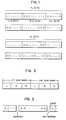
- each of 2 ni code words (1 ⁇ i ⁇ i max ) each consisting of n bits is divided into three blocks, leading block L of the code word, and block R and an intermediate block between the block L and the block R, and in each block, usable code words are selected in accordance with a value uniquely determined for the given d and k, and a uniquely determined concatenation rule of the code words for the selected code words is introduced so that the d, k-constrained RLL code having a higher performance can be readily generated.
- a concatenation portion of the code words means ( ⁇ 1 +l 2 ) bits of the block R of the first code word and the block L of the second code word.
- L B indicates the binary value of the bits in the block R of the first code word.
- ⁇ 1 and l 2 are defined as follows.
- the code word constrained by the equations (4) on the blocks R and L may be used.
- the code words which are constrained by the condition (i) for the block B and the conditions shown by the equations (4) are expressed as ⁇ Cx11 i ⁇ .
- a code word having n i bits-of the same binary value is included in ⁇ CX11 i ⁇ .
- the code word contained in ⁇ CX11 i ⁇ starts with "1" or "0" depending on LB. Accordingly, those code words are grouped to a set (two words) and one data word is assigned to each set of code words.
- the set of code words are combination of a code word which is contained in ⁇ CX11 i ) and which starts with "1" bit (hereinafter referred to as a front pattern) and a code pattern which start with "0" bit with “0" bits and “1” bits of the front pattern being substituted by "1" bits and "0" bits, repectively (hereinafter referred to as a back pattern).
- a front pattern a code word which starts with "0" bit with "0" bits and "1” bits of the front pattern being substituted by "1" bits and "0" bits, repectively
- code words contained in ⁇ CX11 i ⁇ are represented by ⁇ C11 i ⁇ , and a code word consisting of a back pattern C11 i of any code word Cll. contained in ⁇ Cll. ⁇ is represented by ⁇ C11 i ⁇ .
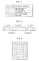
- Fig. 4 shows a relation between the data words and the code words and the concatenation rule of the code words.
- the switching logic for the front pattern and the back pattern can be readily constructed.
- the blocks L and R need not meet the d-constraint but the d-constraint may be not by the concatenation of the code words as shown in a equation (7).
- the d-constraint should be considered if the block R of the first code word and the block L of the second code word have different binary values from each other, and the k-constraint should be considered if those blocks have the same binary value.
- the block R of the first code word comprises "0"s and the block L of the second code word comprises “l”s.
- the second code word is in the front pattern on the back pattern depending on whether the number of continuous bits of the same binary value in the block R of the first code word is no smaller than d or not and whether the binary value LB of the block R of the first code word is "1" or "0", and whether the number of continuous bits of the same binary value in the block L of the second code word is no smaller than dior not. Accordingly, two code words (front pattern and back pattern) are assigned to each data word.
- Fig. 6 shows the concatenation rule of the code words expained in (II.1) and (II.2).
- E 2 is "1” if the number of continuous bits of the same binary value in the block R of the first code word is no smaller than d
- E 2 is "0" if the number is no larger than d-1.
- LB indicates the binary value in the block R of the first code word.
- F 2 is "1' if the number of continuous bits of the same binary value in the block L of the first code word is no smaller than d and F 2 is "0” if the number is no larger than d-1.
- INV2 is "0” if the second code word is the front pattern and INV2 is "1" if the second code word is the back pattern.
- control signal INV 2 for switching the front pattern and the back pattern is given by where "-" represents a logical AND function, " ⁇ " represents an exclusive OR function and "-" represent a NOT function.
- control of switching of the front pattern and the back pattern which appears to be complex at a first glunce can be implemented by the very simple logic as shown by the equation (14) so long as the code words defined by the equation (12) of the present invention are used.
- the RLL codes constructed in accordance with (II) are explained below.
- T of the code is laraer by 21% k is smaller by 15%. Accordingly, this code is much more suitable for high density recording than the HDM-3 code.
- the number of code words contained in ⁇ C20 1 ⁇ , ⁇ C2l i ⁇ and their back patterns increases as N c increases.
- the number of code words contained in ⁇ C20 i ⁇ , ⁇ C2l i ⁇ and their back patterns is maximum when y is selected to maximize the value of N c .
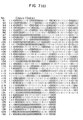
- 5-bit code words No. 1 and No. 2 in Fig. 7 are concatenated in accordance with the concatenation rule of Fig. 5 to obtain the following four bit sequences. Those four bit sequences having the bit length of ten are different from ten-bit code words No. 3 to No. 6 of Fig. 7.
- a 15-bit code word No. 15 is constructed by concatenation of the 10-bit code word No. 5 and a back pattern No. 2 of the 5-bit code word No. 2, as shown below.
- the code words No. 5 and No. 2 are concatenated in the following manner. It is thus seen that the code word No. 15 is not constructed by the concatenation of the code words No. 5 and No. 2.
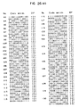
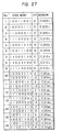
- Data words corresponding to the respective code words are also shown in Fig. 7.
- a ratio of the number of bits of the data word and the number of bits of the code word is constantly 2/5. Accordingly, the code transmission rate is constant and T is constantly equal to 0.4T.
- the assignment-of the data word to the code word is determined in the following manner.
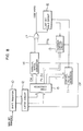
- the content of the latch 12 is equal to a.
- the 12 bits latched in the latch 12 are supplied to an input terminal of a code converter 13.
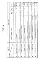
- Fig. 9 shows an input (output table of the code converter 13 of Fig. 8.
- "X" indicates an independent value.
- the code converter 13 may be a read-only memory (ROM).
- Step 2 The I produced in the step 1 is supplied to a control pulse generator 11. The control pulse generator 11 detects that the content of the shift register 10 has been shifted by 2xI bit positions, based on the value of I and generates a control pulse CP.
- F 2 and E 2 are supplied to an inversion control circuit 15.
- F 2 is used together with a value E' of E 2 of the code word CW' immediately previously sent out and the last bit LB of CW' held in a last bit hold circuit 16, and the inversion control circuit 15 produces a signal IVN 2 to instructing whether CW is to be sent out in the back pattern or not, in accordance with the concatenation rule of Fig. 6 and supplies the signal INV 2 to an exclusive OR gate 17.
- INV 2 is defined by the equation (14).
- Step 4 The control pulse CP generated in the step 2 is supplied to the latch circuit 12 in parallel with the step 3 so that new 12 bits are latched into the latch 12.
- the content of the shift register 10 at this moment is 12 bits following to "01” in the equation (16), that is, The content of the latch 12 is also 8.
- the steps 1 to 4 are repeated so that the content of the latch 12 is following to 0111111111111 of the equation (16).
- the steps 1 to 4 are repeated to this value y.
- Fig. 10 shows a time chart of the encoder of Fig. 9 for the data bit sequence of the equation (16). Symbols in Fig. 10 are identical to those used in the description of the steps 0 to 4. Broken lines in Fig. 10 indicate the same time point and "X" indicates an independent value.
- a decoder of the present embodiment is now explained. If a word boundary in the bit sequence generated by the encoder described above is correctly detected, correct decoding is attained.
- the code words used in the present embodiment are those which enable correct determination of word boundaries in the bit sequences created by the concatenation. Accordingly, the decoder is constructed as shown in a block-diagram of Fig. 11. The operation of the decoder is described below.
- Step 0 30 bits from the beginning of the equation (17), that is, are loaded to a 30-bit shift register 30.
- the beginning of the code word may be detected by a known method such as by using a mark pattern.
- Step 1 The 30 bits loaded to the shift register 30 are latched into a 30-bit latch 32 by a control pulse CP from a control pulse generator 31.
- the content of the latch 32 is identical to a'.
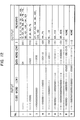
- Fig. 12 shows a portion of an input/output table of the code reverse-converter 33. Blanks in the input column of Fig. 12 show that the reverse conversion is independent from the values in the blank areas. The numbers in the remarks are those assigned to the code words of Fig. 7. If, for example, a 30-bit bit sequence starting with ''11111" is applied to the input of the code reverse-converter 33 of Fig. 11 and if a code word whose number is shown in the remark of Fig. 12 is included in the positions after the first ten bits of the 30-bit sequence, the data word "01" corresponding to the code word "11111" is not outputted. As an example, the code word No. 9 in Fig. 12 is equal to No. 121 in Fig.
- the word boundary of the code words can be correctly determined.
- Step 2 I obtained in the step 1 is supplied to a control pulse generator 31, which detects that the content of the shift register 30 has been shifted by 5xI bits, based on the value of I and generates a control pulse CP.
- Step 4 The control pulse CP generated in the step 2 is applied to the latch 31 in parallel with the step 3 so that new 30 bits are latched.
- the steps 1 to 4 are repeated to obtain a data word "111111111111”.
- the steps 1 to 4 are repeated for the content of the latch 31 of to obtain a data word "111000”.
- the data word for the equation (17) is which is equal to the data bit sequences (A), (B) and (C) of the equation (16) assumed in the description of the operation of the encoder. This means that the correct decoding was attained.
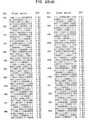
- Fig. 13 also shows examples of data words corresponding to the code words. Those code words are suitable as the variable length code words as is confirmed in the same manner as that of the embodiment 1 and the relation between the data words and the code words is obtained in the same manner as that of the embodiment 1.
- the RLL code of the present embodiment has the same T w and T min as those of the conventional HDM-3 code and has a k which is smaller by 9. Accordingly, it offers a high practial advantage.
- There are 180 code words having a bit length of n min 15 and 19502 code words having a bit length of 30 bits, which are usable in the present embodiment.
- the RLL code of the present embodiment has the same d and k as those of the conventional 3PM code and T w and T min which are longer by approximately 6.7%.
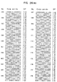
- Fig. 14 also shows examples of data words corresponding to the code words. Those code words are suitable for the variable length code words as is confirmed in the same manner as that in the embodiment 1, and the relation between the data words and the code words is obtained in the same manner as that in the embodiment 1.
- the RLL code of the present embodiment has the same d, T w and T min as those of the conventional 2/3 0162558 conversion code and a k which is smaller by one.
- the present RLL code is more suitable to the high density recording and the high speed transfer than the 2/3 conversion code.
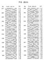
- Fig. 17 also shows data words corresponding to the code words. Those code words are suitable for the variable length code word as is confirmed in the same manner as that in the embodiment 1 and the relation between the data words and the code words is obtained in the same manner as that in the embodiment 1.
- the RLL code of the present embodiment has the same d, k, T and T min as those of the conventional (2, 7) RLLC and the maximum bit length of the code word used is 6 in the present code while it is 8 in the (2, 7) RLLC. Accordingly, a hardware and the encoding and decoding algorithm are simplified. Accordingly, the present RLL code offers a greater advantage than the conventional (2, 7) RLLC.
- the RLL codes of the embodiment so far described include D.C. components and are not well suitable to a VTR having a DC cut off characteristic.
- the second code word which meets the d, k-constraint' and does not increase DSV 2 at the lost bit of the second code word is selected.
- the DSV 2 is no larger than DSV 1 . Accordingly, the data words and the code words have the one-to-one correspondence.
- the code word C10li and its back pattern C10l i are paired and a data word is assigned to the pair because DP 2 must use the code word of the opposite polarity to DSV 1 in order to prevent the increase of DSV 2 since DP ⁇ 0 in ⁇ C10l i ⁇ .
- the four code words CllPi, Cllm i , CllPi and Cllm i are grouped into one set and a data word is assigned to the set.
- the combination of CllPi and CllPi and the combination of Cllm i and Cllm i are provided to meet the d, k-constraint, and the combination of CllPi and C11m i and the combination of CllPi and C11m i serve to prevent the increase of DSV.
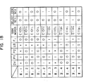
- Fig. 18 shows a rule for the combination and selection of the code words in (III.1) to (III.4).
- a decoder is similar to the variable length RLL code decoder shown in Fig. 11 and hence it is omitted here.
- Fig. 19 shows a block diagram of the encoder. The operation is explained below.
- An m-bit data word is simultaneously applied to both address terminals of an ROM 101 and an ROM 102.
- the ROM 101 contains the code words ⁇ C100 i ⁇ , ⁇ C101 i ⁇ , ⁇ C110 i ⁇ ' ⁇ C11P i ⁇ ' their disparities DP and F 1 .
- the ROM 102 contains the code words ⁇ C11m i ⁇ ' DP and F 1 .
- n-bit code word is supplied to a parallel-serial converter 103 where it is converted to a serial data, which is then supplied directly on one hand and through an inverter 104 on the other hand to a 4-to-1 multiplexer 105.
- an n-bit code word at the output terminal of the ROM 102 is supplied to a parallel-serial converter 106 where it is converted to a serial data, which is supplied directly on one hand and through an inverter 107 on the other hand to the multiplexer 105.
- a code word selector 108 generates a selection signal to select one of the four code words thus generated.
- the selector 108 is constructed in accordance with the equations (21) and (22) and operated in accordance with DP and F 1 from the ROM 101, the last bit LB of the previously sent code word retained in a last bit hold circuit 109 and DSV at the last bit of the previously sent code word. DSV is calculated by the code word selector 108.
- a sample of a video signal is usually quantized to an 8-bit signal, In the present embodiment, such 8-bit digital video signal is directly converted to the DC free RLL code.
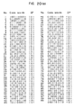
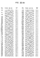
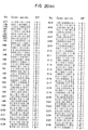
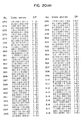
- the code words No. 1 to No. 88 and No. 93 to No. 184 belong to ⁇ C100 i ⁇
- the code words No. 194 to No. 352 belong to ⁇ C101. ⁇ and ⁇ C101 i ⁇
- the code words No. 89 to No. 92 and No. 185 to No. 193 belong to ⁇ C110 i ⁇ and ⁇ C110 i ⁇
- the code word No. 353 belongs to ⁇ C11P i ⁇ ' ⁇ C11P i ⁇ ' ⁇ C11m i ⁇ and ⁇ C11m i ⁇ .
- the DC component is always zero so long as the concatenation rule of Fig. 18 is followed. While the DC component is zero in a long term average, it slightly varies in a short period. Since the variation width relates to the variation width of DSV, the short term DC component variation is small if the DSV variation width is small. Since the DSV variation width is limited by the disparity DP of the code words used, the code words having small
- 2 is not used, one-to-one correspondence to the 8-bit data words is attained. Accordingly, in a circuit configuration to generate the (1, 4) DC free code, the ROM 102, parallel-serial converter 106 and inverter 107 in Fig. 19 are eliminated and the select signal SC, in Fig. 18 is not necessary and the equation (21) is not necessary. Accordingly, the code word selector 108 in Fig. 19 is further simplified.
- x in the equations (3) and (4) are set to 2.
- the conventional 8-bit digital video signal is directly converted to the DC free RLL code and the k is improved by the factor of 2.5.
- Such DC free RLL code can be generated by a very simple circuit. Accordingly, the present embodiment can be applied to the digital video magnetic recording as well as digital audio signal recording.
- the minimum k is 8. Accordingly, the present embodiment allows to reduce k by one.
- This code may be used in the digital video recording.
- T w is longer by 0.12T than that of the known 8/10 conversion code and k is smaller by 3 .
- T w 0.86T.
- T w is longer by 0.06T than that of the known 8/10 conversion code and k is smaller by 6.
- T w 0.89T. Accordingly, T is longer by 0.09T than that of the known 8/10 conversion code and k is smaller by 5.
- T w 0.83T. Accordingly, T w is longer by 0.03T than that of the known 8/10 conversion code and k is smaller by 4.
- DC free RLL codes having even number code word length are used to attain the 2m/2n conversion DC free RLL code so that k is reduced from that of the m/n conversion DC free RLL code while T is kept unchanged and with a smaller memory capacity required for the encoder and decoder than that required when the 2m/2n conversion DC free RLL code is attained by a single code.
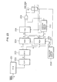
- Fig. 23 shows a block diagram of the encoder of the present embodiment. The operation thereof is described below.
- a conventional video signal is digitally processed, it is quantized to 8-bit video signal which is then supplied to a parallel-serial converter (P/S) 201 of Fig. 23.
- the bit sequence from the parallel-serial converter 201 is converted to a 16-bit parallel data by a serial-parallel converter (S/P) 202.
- S/P serial-parallel converter
- the 16-bit data comprises two 8-bit video signal words.
- the 16-bit data is supplied to a D flip-flop 203, and high order seven bits of the output thereof are applied to an address input terminal of a read-only memory (ROM) 204 while the low order nine bits thereof are applied to an address input terminal of the ROM 205. That is, the 2-word video signal is divided into the high order 7 bits of the first word and the least significant bit of the first word plus the 9 bits of the second word.
- ROM read-only memory
- the ROM 204 outputs 12 bits, that is, an 8-bit code word corresponding to the 7-bit data word, 3 bits indicating the disparity and 1 bit indicating F 1 , and the ROM 205 outputs 14 bits, that is, a 10-bit code word corresponding to the 9-bit data word, 3 bits indicating the disparity and 1 bit indicating F 1 .
- a switching control circuit 206 selects one of the output of the ROM 204 and the output of the R OM 205.
- a switching control signal is directly applied to a chip select terminal of the ROM 204 and applied to a chip select terminal of the ROM 205 through an inverter 207.
- the code word supplied from the ROM 204 or the ROM 205 is supplied to a parallel-serial converter (P/S) 208 in which it is converted to a bit sequence which is then supplied to an exclusive OR gate 209.
- P/S parallel-serial converter
- an inversion control circuit 210 calculates a select code SC2 based on DP and F l of the code word supplied by the ROM 204 or 205, DSV of the immediately previous code word held in the inversion control circuit 210 and the output LB of the D flip-flop which holds the last bit of the immediately previous code word.
- the select code SC2 is then supplied to the exclusive OR gate 209 which determines whether the code word is to be converted to the back pattern or not.
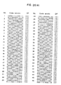
- the DSV is controlled in either the 7/8 conversion or the 9/10 conversion.
- the present embodiment can be implemented by a very simple circuit configuration.
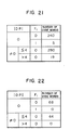
- the number of code words in Fig. 22 is 132 and the number of code words in Fig. 23 is 520 so that both 7/8 conversion and 9/10 conversion can be effected.
- the encoder of the present embodiment is further simplified in configuration.
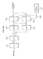
- Fig. 24 shows a decoder of the present embodiment.
- the ROM 303 performs the 8/7 conversion while the ROM 304 performs the 10/9 conversion so that data words corresponding to the input code words are decoded.
- the 7 bits from the ROM 303 and the most significant bit of the ROM 304 are supplied to a D flip-flop 305 while the remaining 8 bits of the output from the ROM 304 are supplied to a D flip-flop 306.
- the 0162558 first word in the code conversion is supplied to the D flip-flop 305 and the second word is supplied to the D flip-flop 306.
- An output selector 307 sequentially outputs the decoded data words. An output thereof is directly applied to an output control terminal of the D flip-flop 305 and applied to an output control terminal of the D flip-flop 306 through an inverter 308.
- the decoder of the present embodiment can be implemented by a very simple circuit configuration.
- two data words are divided into the high order 7 bits of the first word and the 9 bits comprising the least significant bit of the first word and the 9 bits of the second word and those two groups are encoded respectively. Accordingly, the propagation of error due to one-bit error in the communication line to other code word is only the least significant bit of the first word at most. Thus, the influence of the error propagation to the image quality is negligible.
- a code such as DVTR which is suitable for high density recording can be attained with a very simple circuit configuration, the capacity of the ROM can be significantly reduced and the influence by the error propagation is negligible.
- the DC free RLL code of the present embodiment having such characteristics has a high practical value.
- the second code word i.e., a code word to be next outputted
- the second code word is selected, in association with the value DSV 1 resulting with the last bit of the first code word (i.e., a code word outputted just precedently) so as to satisfy the d, k-constraint and not to increase the DSV value for the concatenation to the first code word.
- the code words ⁇ C20 i ⁇ , ⁇ C21 i ⁇ and their back patterns ⁇ C20 i ⁇ , ⁇ C21 i ⁇ are used and the concatenation rule of the code words shown in Fig. 6 is used so that the d, k-constraint is met.
- the following combinations of code words, the relation to the data words and the selection method of the second code word for the DSV 1 for the last bit of the first code word are used.
- Fig. 25 shows combinations of the code words (IV.1) - (IV.4) and the rule for selecting the code words.
- SC1 and SC2 in Fig. 25 are defined as follows. From the equations (23) and (24), SC1 is represented by The equations (24) and (25) are actual select code generation logics.
- the DV in Fig. 25 is a sign bit of the D SV and the P in F ig. 25 is derived from an inversion of a logical OR function of all bits of the disparity of the code word.
- the DC free RLL code for d > 2 in the present embodiment can be implemented by a very simple configuration.
- the 8-bit data word is directly converted to the code word.
- code words No. 1 - No. 26 and No. 59 - 82 belong to the code words ⁇ 200 i ⁇ and ⁇ 200 i ⁇
- the code words No. 27 - No. 58 and No. 83 - No. 121 belong to the code words ⁇ 210 i ⁇ and ⁇ 210 i ⁇
- the DC free RLL code of the present embodiment has 14% longer T w than the conventional 8/16 conversion code and is suitable for higher density recording.
- Each set includes code words having DP > 0 and DP ⁇ 0 respectively, so that the divergence of DSV can be prevented by selectively using the code word having DP of the opposite sign to that of DSV 1 in a similar way to the cases of (IV.3) and (IV.4).
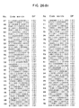
- the code word No. 16 is one by the combination (IV.5.2) of the new code words.
- the combination of code words in Fig. 26 is just an example.
- d and T w are equal to those in the conventional 8/16 conversion DC free RLL code and k is larger by 3.
- the code length is one half and a memory capacity required for the encoder and the decoder is signifcantly reduced.
- the code word is divided into three blocks L, B and R and constraints for the blocks L, B and R which are uniquely defined for given d and k are introduced.
- the RLL codes can be readily constructed. Many of the RLL codes thus constructed have higher performance than the conventional RLL code.
- the present invention provides method and apparatus which are very advantageous to construct the effective RLL code.
Landscapes
- Engineering & Computer Science (AREA)
- Signal Processing (AREA)
- Compression, Expansion, Code Conversion, And Decoders (AREA)
- Signal Processing For Digital Recording And Reproducing (AREA)
Applications Claiming Priority (4)
| Application Number | Priority Date | Filing Date | Title |
|---|---|---|---|
| JP102138/84 | 1984-05-21 | ||
| JP59102138A JPS60246155A (ja) | 1984-05-21 | 1984-05-21 | 符号変換方法 |
| JP59186705A JPS6165531A (ja) | 1984-09-06 | 1984-09-06 | 符号変換方法 |
| JP186705/84 | 1984-09-06 |
Publications (3)
| Publication Number | Publication Date |
|---|---|
| EP0162558A2 true EP0162558A2 (fr) | 1985-11-27 |
| EP0162558A3 EP0162558A3 (en) | 1987-02-25 |
| EP0162558B1 EP0162558B1 (fr) | 1991-08-21 |
Family
ID=26442873
Family Applications (1)
| Application Number | Title | Priority Date | Filing Date |
|---|---|---|---|
| EP85302291A Expired EP0162558B1 (fr) | 1984-05-21 | 1985-04-02 | Méthode et appareil pour la génération d'un code à longueur de course limitée |
Country Status (3)
| Country | Link |
|---|---|
| US (1) | US4760378A (fr) |
| EP (1) | EP0162558B1 (fr) |
| DE (1) | DE3583819D1 (fr) |
Cited By (4)
| Publication number | Priority date | Publication date | Assignee | Title |
|---|---|---|---|---|
| EP0392506A3 (fr) * | 1989-04-12 | 1991-10-30 | Nippon Hoso Kyokai | Méthode de modulation digitale |
| EP0571905A3 (fr) * | 1992-05-25 | 1995-06-07 | Sony Corp | Procédé de modulation. |
| GB2315650A (en) * | 1996-07-23 | 1998-02-04 | Samsung Electronics Co Ltd | Run length limited coding method |
| EP4142229A1 (fr) * | 2021-08-31 | 2023-03-01 | Samsung Display Co., Ltd. | Système et procédé de codage de transition avec taille de mot flexible |
Families Citing this family (37)
| Publication number | Priority date | Publication date | Assignee | Title |
|---|---|---|---|---|
| US4985700A (en) * | 1988-03-01 | 1991-01-15 | Canon Kabushiki Kaisha | Variable-length coding/decoding device |
| US5486828A (en) * | 1989-04-06 | 1996-01-23 | Canon Kabushiki Kaisha | Coding/decoding method and apparatus therefor |
| US5184125A (en) * | 1989-06-28 | 1993-02-02 | Digital Equipment Corporation | Data encoding and demodulation system |
| JPH03105769A (ja) * | 1989-09-20 | 1991-05-02 | Matsushita Electric Ind Co Ltd | 情報再生装置 |
| AU624274B2 (en) * | 1989-11-20 | 1992-06-04 | Digital Equipment Corporation | Data format for packets of information |
| JPH04225625A (ja) * | 1990-12-27 | 1992-08-14 | Sony Corp | ディジタル変調方式 |
| US5349350A (en) * | 1991-10-31 | 1994-09-20 | Integral Peripherals, Inc. | Run length limited encoding/decoding system for low power disk drives |
| US5625644A (en) * | 1991-12-20 | 1997-04-29 | Myers; David J. | DC balanced 4B/8B binary block code for digital data communications |
| JP3541439B2 (ja) * | 1994-07-08 | 2004-07-14 | ソニー株式会社 | 信号変調方法及び装置、並びに信号復調装置及び方法 |
| US5537382A (en) * | 1994-11-22 | 1996-07-16 | Optex Corporation | Partial response coding for a multi-level optical recording channel |
| JP3243140B2 (ja) * | 1995-02-20 | 2002-01-07 | パイオニア株式会社 | データ変換方式 |
| KR100231379B1 (ko) * | 1995-04-12 | 1999-11-15 | 니시무로 타이조 | 코드 변환/복호 장치 및 방법 |
| US5574448A (en) * | 1995-05-08 | 1996-11-12 | Quantum Corporation | Method and apparatus for encoding data with variable block lengths |
| US5663723A (en) * | 1995-05-12 | 1997-09-02 | Optex Corporation | M=7 (1,3) runlength limited code for multi-level data |
| US5659311A (en) * | 1995-05-12 | 1997-08-19 | Optex Corporation | M=6 (2,4) runlength limited code for multi-level data |
| US5663722A (en) * | 1995-05-12 | 1997-09-02 | Optex Corporation | M=10 (3,6) runlength limited code for multi-level data |
| US5668546A (en) * | 1995-05-12 | 1997-09-16 | Optex Corporation | M=6 (3,6) runlength limited code for multi-level data |
| US5757293A (en) * | 1995-05-12 | 1998-05-26 | Optex Corporation | M=8 (1,2) runlength limited code for multi-level data |
| US5748118A (en) * | 1995-05-12 | 1998-05-05 | Optex Corporation | M=7 (3,8) runlength limited code for multi-level data |
| US5659310A (en) * | 1995-05-12 | 1997-08-19 | Optex Corporation | M=5 (0,2) runlength limited code for multi-level data |
| US5748117A (en) * | 1995-05-12 | 1998-05-05 | Optex Corporation | M=8 (1,3) runlength limited code for multi-level data |
| US5781130A (en) * | 1995-05-12 | 1998-07-14 | Optex Corporation | M-ary (d,k) runlength limited coding for multi-level data |
| US5657014A (en) * | 1995-05-12 | 1997-08-12 | Optex Corporation | M=7 (3,7) runlength limited code for multi-level data |
| US5682155A (en) * | 1995-05-12 | 1997-10-28 | Optex Corporation | M=6(4,11) runlength limited code for multi-level data |
| US5680128A (en) * | 1995-05-12 | 1997-10-21 | Optex Corporation | M=6(3,8) runlength limited code for multi-level data |
| US5682154A (en) * | 1995-05-12 | 1997-10-28 | Optex Corporation | M=4 (1,2) runlength limited code for multi-level data |
| US5675330A (en) * | 1995-05-12 | 1997-10-07 | Optex Corporation | M=5(4,11)runlength limited code for multi-level data |
| US5670956A (en) * | 1995-05-12 | 1997-09-23 | Optex Corporation | M=5 (3,7) runlength limited code for multi-level data |
| US5859601A (en) * | 1996-04-05 | 1999-01-12 | Regents Of The University Of Minnesota | Method and apparatus for implementing maximum transition run codes |
| WO1997050179A1 (fr) * | 1996-06-24 | 1997-12-31 | Etom Technologies Corporation | Code limite par longueur de ligne de type m=10 (2,10), d=3.75 pour donnees a plusieurs niveaux |
| US6229462B1 (en) * | 1999-03-30 | 2001-05-08 | Intel Corporation | Method and apparatus for reducing the disparity of set and clear bits on a serial line |
| KR100336496B1 (ko) * | 1999-08-20 | 2002-05-15 | 오길록 | 무직류, 최소대역폭특성을 갖는 선로부호의 설계방법 및 부호화/복호화 장치 |
| US6967597B1 (en) * | 2000-11-08 | 2005-11-22 | Lg Electronics, Inc. | Method and apparatus for coding information, method and apparatus for decoding information, method of fabricating a recording medium, the recording medium and modulated signal |
| KR100421004B1 (ko) * | 2001-04-20 | 2004-03-03 | 삼성전자주식회사 | 코드 생성 및 배치 방법 |
| KR100552699B1 (ko) * | 2003-10-27 | 2006-02-20 | 삼성전자주식회사 | 코드율 7/8인 mtr 코드 부호화/복호화 방법 및 장치 |
| US7230550B1 (en) * | 2006-05-16 | 2007-06-12 | Motorola, Inc. | Low-complexity bit-robust method and system for combining codewords to form a single codeword |
| US10439639B2 (en) | 2016-12-28 | 2019-10-08 | Intel Corporation | Seemingly monolithic interface between separate integrated circuit die |
Family Cites Families (6)
| Publication number | Priority date | Publication date | Assignee | Title |
|---|---|---|---|---|
| US3689899A (en) * | 1971-06-07 | 1972-09-05 | Ibm | Run-length-limited variable-length coding with error propagation limitation |
| US4146909A (en) * | 1977-11-21 | 1979-03-27 | International Business Machines Corporation | Sync pattern encoding system for run-length limited codes |
| US4398225A (en) * | 1981-04-24 | 1983-08-09 | Iomega Corporation | Combined serializer encoder and decoder for data storage system |
| US4501000A (en) * | 1981-07-27 | 1985-02-19 | Sony Corporation | Method of coding binary data |
| JPS5875353A (ja) * | 1981-10-29 | 1983-05-07 | Pioneer Electronic Corp | デ−タ変換方式 |
| US4486739A (en) * | 1982-06-30 | 1984-12-04 | International Business Machines Corporation | Byte oriented DC balanced (0,4) 8B/10B partitioned block transmission code |
-
1985
- 1985-04-02 DE DE8585302291T patent/DE3583819D1/de not_active Expired - Lifetime
- 1985-04-02 EP EP85302291A patent/EP0162558B1/fr not_active Expired
- 1985-04-03 US US06/719,629 patent/US4760378A/en not_active Expired - Lifetime
Cited By (8)
| Publication number | Priority date | Publication date | Assignee | Title |
|---|---|---|---|---|
| EP0392506A3 (fr) * | 1989-04-12 | 1991-10-30 | Nippon Hoso Kyokai | Méthode de modulation digitale |
| EP0571905A3 (fr) * | 1992-05-25 | 1995-06-07 | Sony Corp | Procédé de modulation. |
| GB2315650A (en) * | 1996-07-23 | 1998-02-04 | Samsung Electronics Co Ltd | Run length limited coding method |
| GB2315650B (en) * | 1996-07-23 | 1998-06-17 | Samsung Electronics Co Ltd | Signal modulation method employing multilevel run length limit coding scheme |
| US5892467A (en) * | 1996-07-23 | 1999-04-06 | Samsung Electronics Co., Ltd. | Signal modulation method employing multilevel run length limit coding scheme |
| EP4142229A1 (fr) * | 2021-08-31 | 2023-03-01 | Samsung Display Co., Ltd. | Système et procédé de codage de transition avec taille de mot flexible |
| US11637685B2 (en) | 2021-08-31 | 2023-04-25 | Samsung Display Co., Ltd. | System and method for transition encoding with flexible word-size |
| US11888962B2 (en) | 2021-08-31 | 2024-01-30 | Samsung Display Co., Ltd. | System and method for transition encoding with flexible word-size |
Also Published As
| Publication number | Publication date |
|---|---|
| US4760378A (en) | 1988-07-26 |
| DE3583819D1 (de) | 1991-09-26 |
| EP0162558A3 (en) | 1987-02-25 |
| EP0162558B1 (fr) | 1991-08-21 |
Similar Documents
| Publication | Publication Date | Title |
|---|---|---|
| EP0162558B1 (fr) | Méthode et appareil pour la génération d'un code à longueur de course limitée | |
| US4677421A (en) | Digital information signal encoding method with reduced run length and improved self-clocking | |
| US4626826A (en) | Method and apparatus for encoding and decoding an NRZI digital signal with low DC component and minimum low frequency components | |
| US4833470A (en) | Code conversion apparatus | |
| BG64243B1 (bg) | Метод и устройство за модулация/демодулация с последователно ограничаване на минималната дължина на серия от еднакви знаци в кодова дума | |
| US6127951A (en) | Modulating device, modulating device, demodulating device, demodulating device, and transmission medium run length limited coder/decoder with restricted repetition of minimum run of bit sequence | |
| EP0557130B1 (fr) | Méthode de conversion de données et appareil d'enregistrement/de reproduction l'utilisant | |
| US4672362A (en) | Binary data encoding and decoding process | |
| US4496934A (en) | Encoding and decoding systems for binary data | |
| US4988999A (en) | Digital modulation method | |
| EP0932258B1 (fr) | Procede et circuit de modulation numerique et procede et circuit de demodulation numerique | |
| EP0090047B1 (fr) | Systeme de codage et de decodage pour des donnees binaires | |
| GB2067055A (en) | Methods of converting binary digital information | |
| US4881076A (en) | Encoding for pit-per-transition optical data recording | |
| JP2003536315A (ja) | バイナリのソース信号のデータビットのストリームをバイナリのチャネル信号のデータビットのストリームに符号化するデバイス、メモリ手段、情報を記録するデバイス、記録担体、符号化するデバイス、および再生するデバイス | |
| KR20020011981A (ko) | 정보 코딩을 위한 장치 및 방법과, 그 코딩된 정보를디코딩하기 위한 장치 및 방법과, 변조신호 및 기록매체제조방법 | |
| US6477209B1 (en) | Method for encoding and decoding recording codes and method for inserting synchronization signals | |
| KR100470026B1 (ko) | 정보를 코딩/디코딩하는 방법 및 장치 | |
| KR100752880B1 (ko) | 정보를 코딩/디코딩하는 방법 및 장치 | |
| KR20010041155A (ko) | 엔-비트 소스어를 대응하는 엠-비트 채널어로 인코딩하고, 엠-비트 채널어를 대응하는 엔-비트 소스어로 디코딩하는 장치 | |
| KR0185944B1 (ko) | (1,7)변조코드를 이용하는 복호화방법 및 그 장치 | |
| JP2573067B2 (ja) | 情報変換装置 | |
| KR100575658B1 (ko) | 정보 코딩을 위한 장치 및 방법 | |
| JP2004514367A (ja) | 情報の符号化のための装置及び方法、その符号化された情報を復号するための装置及び方法、変調信号及び記録媒体の製造方法 | |
| JPS63204822A (ja) | 符号変換装置 |
Legal Events
| Date | Code | Title | Description |
|---|---|---|---|
| PUAI | Public reference made under article 153(3) epc to a published international application that has entered the european phase |
Free format text: ORIGINAL CODE: 0009012 |
|
| AK | Designated contracting states |
Designated state(s): DE FR GB |
|
| PUAL | Search report despatched |
Free format text: ORIGINAL CODE: 0009013 |
|
| AK | Designated contracting states |
Kind code of ref document: A3 Designated state(s): DE FR GB |
|
| 17P | Request for examination filed |
Effective date: 19870707 |
|
| 17Q | First examination report despatched |
Effective date: 19881215 |
|
| GRAA | (expected) grant |
Free format text: ORIGINAL CODE: 0009210 |
|
| AK | Designated contracting states |
Kind code of ref document: B1 Designated state(s): DE FR GB |
|
| REF | Corresponds to: |
Ref document number: 3583819 Country of ref document: DE Date of ref document: 19910926 |
|
| ET | Fr: translation filed | ||
| PLBE | No opposition filed within time limit |
Free format text: ORIGINAL CODE: 0009261 |
|
| STAA | Information on the status of an ep patent application or granted ep patent |
Free format text: STATUS: NO OPPOSITION FILED WITHIN TIME LIMIT |
|
| 26N | No opposition filed | ||
| PGFP | Annual fee paid to national office [announced via postgrant information from national office to epo] |
Ref country code: DE Payment date: 19940408 Year of fee payment: 10 |
|
| PGFP | Annual fee paid to national office [announced via postgrant information from national office to epo] |
Ref country code: FR Payment date: 19940411 Year of fee payment: 10 |
|
| PG25 | Lapsed in a contracting state [announced via postgrant information from national office to epo] |
Ref country code: FR Effective date: 19951229 |
|
| PG25 | Lapsed in a contracting state [announced via postgrant information from national office to epo] |
Ref country code: DE Effective date: 19960103 |
|
| REG | Reference to a national code |
Ref country code: FR Ref legal event code: ST |
|
| PGFP | Annual fee paid to national office [announced via postgrant information from national office to epo] |
Ref country code: GB Payment date: 19980324 Year of fee payment: 14 |
|
| PG25 | Lapsed in a contracting state [announced via postgrant information from national office to epo] |
Ref country code: GB Free format text: LAPSE BECAUSE OF NON-PAYMENT OF DUE FEES Effective date: 19990402 |
|
| GBPC | Gb: european patent ceased through non-payment of renewal fee |
Effective date: 19990402 |