EP0143887A2 - Verbreiterte IMPATT Struktur - Google Patents
Verbreiterte IMPATT Struktur Download PDFInfo
- Publication number
- EP0143887A2 EP0143887A2 EP84109043A EP84109043A EP0143887A2 EP 0143887 A2 EP0143887 A2 EP 0143887A2 EP 84109043 A EP84109043 A EP 84109043A EP 84109043 A EP84109043 A EP 84109043A EP 0143887 A2 EP0143887 A2 EP 0143887A2
- Authority
- EP
- European Patent Office
- Prior art keywords
- diode
- impatt
- distributed
- active region
- transmission line
- Prior art date
- Legal status (The legal status is an assumption and is not a legal conclusion. Google has not performed a legal analysis and makes no representation as to the accuracy of the status listed.)
- Withdrawn
Links
Images








Classifications
-
- H—ELECTRICITY
- H10—SEMICONDUCTOR DEVICES; ELECTRIC SOLID-STATE DEVICES NOT OTHERWISE PROVIDED FOR
- H10D—INORGANIC ELECTRIC SEMICONDUCTOR DEVICES
- H10D86/00—Integrated devices formed in or on insulating or conducting substrates, e.g. formed in silicon-on-insulator [SOI] substrates or on stainless steel or glass substrates
- H10D86/80—Integrated devices formed in or on insulating or conducting substrates, e.g. formed in silicon-on-insulator [SOI] substrates or on stainless steel or glass substrates characterised by multiple passive components, e.g. resistors, capacitors or inductors
-
- H—ELECTRICITY
- H10—SEMICONDUCTOR DEVICES; ELECTRIC SOLID-STATE DEVICES NOT OTHERWISE PROVIDED FOR
- H10D—INORGANIC ELECTRIC SEMICONDUCTOR DEVICES
- H10D8/00—Diodes
- H10D8/40—Transit-time diodes, e.g. IMPATT or TRAPATT diodes
-
- H—ELECTRICITY
- H10—SEMICONDUCTOR DEVICES; ELECTRIC SOLID-STATE DEVICES NOT OTHERWISE PROVIDED FOR
- H10W—GENERIC PACKAGES, INTERCONNECTIONS, CONNECTORS OR OTHER CONSTRUCTIONAL DETAILS OF DEVICES COVERED BY CLASS H10
- H10W44/00—Electrical arrangements for controlling or matching impedance
- H10W44/20—Electrical arrangements for controlling or matching impedance at high-frequency [HF] or radio frequency [RF]
-
- H—ELECTRICITY
- H10—SEMICONDUCTOR DEVICES; ELECTRIC SOLID-STATE DEVICES NOT OTHERWISE PROVIDED FOR
- H10W—GENERIC PACKAGES, INTERCONNECTIONS, CONNECTORS OR OTHER CONSTRUCTIONAL DETAILS OF DEVICES COVERED BY CLASS H10
- H10W44/00—Electrical arrangements for controlling or matching impedance
- H10W44/20—Electrical arrangements for controlling or matching impedance at high-frequency [HF] or radio frequency [RF]
- H10W44/203—Electrical connections
- H10W44/216—Waveguides, e.g. strip lines
Definitions
- the present invention relates to solid-state microwave devices including oscillators, amplifiers, phase shifters, and attenuators.
- the present invention relates to Avalanche-Transit-Time Devices.
- Avalanche Transit-Time Devices provide a negative resistance which can in principle be used to operate at extremely high microwave frequencies, since the transit time which limits the frequency response is a transit time in a vertical direction, and can be therefore controlled by layer thickness.
- these devices are in principle capable of high power densities at extreme microwave and millimeter frequencies.
- the theoretical potential of such structures has in the past proved difficult to take advantage of, largely due to problems of external impedance matching, which have made it difficult to effectively couple power out of these devices, which are typically fabricated physically small to increase impedance levels.
- the individual IMPATTs (or other Avalanche' Transit-Time Diode type) are physically tiny, (area being inverselv proportional to frequency) and their assembly in a power-combining package will therefore typically contain significant mismatches due to assembly error, which lowers the maximum number of diodes which can be combined. It has therefore been difficult to combine enough IMPATTs to get usefully large amounts of power out at higher microwave and millimeter-wave frequencies, e.g. 94 GHz.
- a further important consideration in the art of Avalanche Transit-Time Devices is that such devices are tvpically quite noisy. Thus, when such a device is to be used, e.g. as a local oscillator, the filtering which is required for reduction of device noise will impose significant additional loses on the already minimal output power of the device. Thus, output power for Avalanche Transit-Time Devices is generally at a premium.
- a distributed IMPATT structure power is coupled out through a side contact. That is , in previously proposed distributed IMPATT structures the gain medium (the active region of the IMPATT) operates as a transmission line.
- the prior art has attempted to couple output power from the gain medium through- an end contact, ie through a contact which intercepts the primary direction of energy propagation (and also to the direction of maximum elongation) of the active medium.
- a side contact extends along the whole active region in a direction which is parallel to the principal direction of propagation of the energy in the active medium.
- the sidewall contact plus the active region together can be considered as a single transmission line.
- the present invention can be configured both as oscillators and as amplifiers.
- When configured as an oscillator multiple short active regions can be sequentially coupled to a single long microstrip, which serves as the sidewall contact for each of the active regions.
- This very simple power combining scheme provides extremely high power at millimeter wave frequencies.
- a microwave device comprising:
- the present invention relates to a voltage-controlled oscillator (VCO) for operation at millimeter-wave frequencies (above 30 GHz).
- VCO voltage-controlled oscillator
- VCO voltage-controlled oscillators
- Numerous methods have been used in the microwave art to configure voltage-controlled oscillators (VCO).
- VCOs are essential to many microwave applications, such as chirped radar and electronic counter measures, in addition to the general utility of VCOs as circuit elements.
- an important limitation of many prior-art microwave VCOs is frequency range and frequency agility. That is, conventional microwave means such as YIG-tuned oscillators, have important frequency limitations.
- a further difficulty with the prior art voltage-controlled oscillator circuits is their parasitic reactance. That is, where -an active element must be connected to a resonating circuit containing a variable-reactance element, the connections themselves become sources of trouble at millimeter-wave frequencies. That is, it is very difficult to design any connection scheme which will not introduce major and uncertain amounts of reactance, and which will not provide substantial resistive and radiation losses.
- a further important desideratum in microwave VCOs is frequency agility. That is, the techniques -which are required for high-frequency voltage-controlled oscillation are not always compatible with extreme frequency agility. However, frequency agility is itself necessary for many electronic counter measure applications, and is highly desirable for many chirped radar applications.
- An integrated low-loss millimeter-wave phase shifter is also useful for many applications, particularly phased array radar.
- the present invention is not by any means limited to distributed IMPATT diodes, but is in general applicable to a distributed realization of any 2-terminal device with gain. That is, applicable device types which may be realized in a distributed mode include not only IMPATTs and other Avalanche Transit-Time Devices (such as BARITTs, TUNNETTs, MITTATs, DOVATTs, heterojunction IMPATTs, etc.), but also transferred- electron devices (Gunn diodes, oscillators, etc.) and tunnel diodes.
- the presently preferred embodiment uses an IMPATT diode, and this embodiment will be discussed primarily. It should be noted that IMPATT diodes have a particular advantage of good high-frequency characterisics and are preferable to many of the other 2-terminal device types for this reason.
- the scope of the present' invention is not limited except as specified in the Claims.
- a distributed IMPATT is basically a long strip of IMPATT diode.
- the depletion layer becomes a parallel plate wave guide which supports a travelling-wave. Due to the distributed nature of the device, the power-frequency limitations associated with lumped diodes do not apply. The devices can therefore be made much larger in area than the conventional IMPATTs giving high power handling capabilitiesitv.
- the IMPATT structure is of single-drift type with the drift region 8 made of n-type GaAs.
- the depletion region terminals (p+ and n+ layers 6 and 4 respectively) form the boundary for the waveguide.
- the device is shunt resonated at the depletion layer boundries, taking full advantage of the high negative conductance of the active layer.
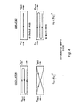
- the parallel connected -R and Cd represent a lumped IMPATT.
- R is usually -500 or larger.
- a load with positive real part and inductive imaqinary part is needed. This is supplied by waveguide cavities.However, looking from the circuitside, this IMPA TT is a series combination of negative resistance R' and Cd ( Figure 2b) where R' is about -5 .
- Rs which. includes all the losses in the circuit and the diode as well as the load resistance, must be smaller than R'. In order to increase R' the diode area is made very small and this in turn limits the power output.
- the waveguide is the depletion layer of the IMPATT and therefore it-is shunt resonated as shown in 2c.
- Cd and L components will be made to have equal magnitudes and Rs will now be limited by neqative resistance R which is much larger than R'. Therefore, devices do not have to be small and no external resonant circuit is needed.
- Distributed IMPA T Ts can best be produced in a monolithic form for ease in manufacturing and integration.
- the length and the width of the device are typically 1-5 mm and 10-100 microns respectively. This represents no particular problem in production.
- a tapered impedance transformer can be produced on semi-insulating (SI) GaAs to match the load and the device impedances. It is possible to use microstrip lines on 4 mil thick SI GaAs substrate up to at least 100 GHz, and even higher on thinner substrates.
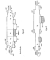
- Figure 10 shows a sectional view of a monolithic distributed device according to the present invention.
- a substrate 10 is provided, such as semi-insulating GaAs.
- Semi-insulating GaAs is preferred because it provides for convenient integration of a distributed device of the present invention with other monolithic microwave integrated circuit components such as FETs, varactors, etc.
- other substrates may be preferred for heat sinking.
- alternative embodiments of the present invention could also be formed as miniature hybrid structures on diamond, copper, B eO, silver, or thick gold-plated substrate. (In these cases the fabrication process is different, preferably using an AlGaAs etch stop to permit patterning of the contact layers).
- the importance of heat-sinking depends partlv on the operation mode: that is, a pulse-mode operation at a low duty cvcle imposes less stringent requirements on heat-sinking than high-duty-cycle or cw applications.
- n+ layer 20 and an active device region 16 are formed by molecular beam epitaxy.
- these layers are deposited by molecular beam epitaxy.
- other methods well known to those skilled in the art may be used to form the structure.
- the semiconductor layers in the active region 16 of the device of the present invention are not themselves novel, and a wide variety of prior-art semiconductor structures may be used.
- the presently preferred embodiment uses a conventional double-drift IMPATT structure, wherein a backside contact layer 20 which is heavily doped is overlaid by an n-tvpe drift region 22, a p- type drift region 24, and a p+ contact region 26.
- the drift regions 22 and 24 are each about 300 nano-meters thick. This thickness will be preferably scaled according to frequency, as as well known to those still in the art. For example, for operation at 94 GHz, the layers 22 and 24 would each be approximately 200 nanometers thick, and of higher doping density. In the presently preferred embodiment, the doping density of the layers 22 and 24 is each approximately 2E17 per cc, but, as is well known to those skilled in the art, different doping levels can be chosen. The doping and thickness of these layers are preferably chosen so that the depletion layer surrounding the junction between layers 22 and 24 spreads just to the edge of the contact layers 20 and 26 at the breakdown voltage (which is lower than the operating voltage).
- the p+ layer 26 is reasonably thin, e.g. 200 nm, but this thickness could be varied. It is essential that the p+ contact layer 26 be thinner than the skin depth at frequencies of interest, but this is not a difficult constraint, since, for GaAs, the skin depth at 94 GHz is several microns.
- the n+ contact layer 20 is preferably thick, but this is done for convenience in the device fabrication steps used.
- a double mesa structure is preferably used. That is, after all layers through layer 26 are deposited, the first mesa etch step is performed to define a large mesa. The large mesa corresponds to the width shown for contact layer 20 in Figure 10.
- a second mesa etch is then performed to remove the active region 16 (i.e. layers 22, 24, and 26) from the portion of n+ contact layer. 20 where the ground contact metallization 18 is typically deposited.
- a silicon nitride layer 12 is deposited and patterned, and a side contact 14 and ground contact 18 are patterned to provide front and back contacts to the Eour-laver structure shown in Figures 11 and 12.
- the back-side metallization 22 is provided merely as an Rf ground plane, and to assist heat-sinking and mounting.
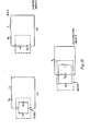
- FIG. 2 A plan view of the distributed device according to the present invention is shown in Figure 2.
- the view shown in Figure 10 corresponds to a sectional view along section a-a in Figure 2.
- a side coupler 14 operates as a transmission line, propagating energy in the direction shown by the arrow.
- the side coupler of 14 can itself be converted to a microstrip line, and provide coupling to other circuit elements.
- FIG 3. One example of a monolithic microwave circuit incorporating the distributed diode of the present invention is shown in Figure 3.
- the-diode active region 16 is highly elongated.
- this diode is 10 microns wide, but maybe millimeters in length.
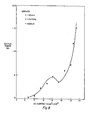
- the fundamental resonant frequency of a diode is determined by its length, as shown in Figure 6.
- the relation between single pass gain and the endpoint reflection coefficent determines whether a simple diode will act as an oscillator or an amplifier. If the single-pass voltage reflection coefficent squared is equal to the single-pass gain, the device will settle into a standing wave condition and will function as an oscillator. That is, if the single pass gain initially exceeds the reflection coefficent squared, the signal levels within the device rise until saturation begins to limit the gain, so that the equality condition is satisfied. On the other hand, if the reflection coefficent squared exceeds the single-pass gain, then the device will function as a multi-pass amplifier. If the reflection coefficent greatly exceeds the single-pass gain, then the amplification will effectively be sinqle-pass amplification.
- Figure 6 shows some sample implementations of the present invention, indicating the dependence of the fundamental mode of oscillating frequency on the device length. As noted, it is preferable to optimize the thickness of the drift regions (the lightly doped region between the heavily doped contact layers in an IMPATT device) for the operating frequency desired.
- the resonant frequency is somewhat sensitive to the thickness and doping of the contact layers 20 and 26. These contact layers load the transmission line, and therefore can lower the phase velocity of propagation in the transmission line, which lowers the resonant frequencv.
- the side coupling microstrip characteristic impedance may need to be small.
- lambda corresponds to the wavelength in the microstrip at the center frequency of frequency band.
- Multi-section transformers give broader band impedance matching.
- Similar lambda/4 transformer sections increase the characteristic impedance level at the output terminal.
- Figure 16 shows this configuration; preferably the impedances increase geometrically.
- DIMPATT width For specific applications it may be desirable to change DIMPATT width; in other words, use wider devices 10 closer to the output end, to ensure that each device 108 or 110 experiences similar power densities. In this case it may be desirable to couple the devices 108 closer to the input port at a different impedance level than those 110 closer to the output, as shown in Figure 17.
- similar size diodes can be used, but with the coupling changed towards the output. This can be achieved, as shown in Figure 18, by again changing the characteristic impedance of the microstrip. Near the input port, better impedance match is supplied, so that the device 108 is strongly coupled to microstrip portion 112. The second device 108 is less strongly coupled to microstrip portion 114, and the last device is weakly coupled to microstrip portion 116.
- Another way of ensuring single pass amplification activity is to use a magnetic field with a ferrite substrate, to ensure directionality. That is, as is well known in the art, if the substrate 10 is made of a ferrimagnetic material, and a dc bias magnetic field is applied normal to the plane of the substrate, wave propogation will preferentially occur in one. direction, so that the device of the present invention will simply act as a single-pass 2 port-amplifier.
- the sidewall coupler 14 can be extended to provide a microstrip transmission line, with a plurality of active regions 16 spaced along it.
- the active region 16 As the active region 16 is made wider, the power handling capacity naturally increases. However, if the active region 16 is made too wide, the characteristic impedance of the device becomes small and effective impedance matching at input/output ports becomes more difficult.
- a practical upper limit for device length is about one tenth of one wavelength of the electromagnetic wave propagating in the device.
- length/width ratio should be kept as large as possible to reduce thermal impedance withoutexceeding the specific limits imposed on the device length.
- Devices operating as oscillators need to be of specific lengths whereas those operating as amplifiers, phase shifters or attenuators can be of varyinq length depending on application needs. 'The gain of an amplifier, the phase shift of a phase shifter., or the attenuation of an attenuator is a strong function of device length.
- the device length should be chosen such that the IMPATT action cannot supply adequate gain at the frequency which would be suitable for oscillators dictated bv device length.
- the key teaching of the present invention is that power is coupled out of a distributed negative resistance diode using a side contact which is coupled to the diode along substantially all of the length of the diode active region.
- This teaching which has fundamental novelty, can be modified and varied to' provide a wide range of embodiments. While the most preferred embodiments couple the distributed IMPATT to a microstrip line having a propagation direction parallel to the long direction of the diode, as shown in Figure 3, embodiments such as Figures 19 and 20 couple the IMPATT to a wide microstripe line extending normal to the long dimension of the diode.
- the side contact of the distributed diode of the present invention can be d.c. coupled as a microstrip transmission line, but it is alternatively possible to capacitatively couple the contact 206 (which extends along diode 208) through a dielectric 210 to a microstrip transmission line 204, as shown in Figure 21.
- the Q of the distributed_IMPATT is lowered, and the distributed IMPATT device can therefore be injection locked over a wide frequency range.
- Additional devices can be coupled with the same microstripe line.
- isolators may be inserted between the distributed IMPATT devices.
- the present invention provides a fundamental innovation in the art of microwave devices, having as advantages all of the above enumerated objects of the invention. While the present invention has been described with reference to one particular embodiment, it teaches a general concept of very broad applicability. The present invention is therefore not limited except as specified in the accompanying Claims, which are to be construed broadly.
- This distributed oscillator structure is adapted to form a distributed VCO, simply by including a variable capacitance element in the transmission line. That is, as seen in Figure 22, the sidewall contact 301 of the distributed IMPATT 303 (or other distributed oscillator) is also attached as one terminal of a (preferably distributed) variable capacitance.
- This variable capacitance 302 has a back bias contact 304, and, by varying the bias on the distributed capacitor of 302, the loading on the transmission line can be chanqed.
- This means that the phase velocity on a transmission line is changed, and this in turn means that the oscillation frequency of a fixed-length cavity will also change. However, the cavity will still be resonanting in its fundamental mode, and will still therefore provide a highly stable high-Q oscillator.
- the oscillator will acquire a new resonant frequency in only a few cavity transit times. This means that such an oscillator has extreme frequency agility and stability.
- this is configured with a distributed IMPATT structure as described above.
- An air bridge 306 connects the sidewall contact of a distributed IMPATT structure to a distributed varactor structure 302. (Alternatively bridge 306 may be supported by a solid dielectric 307 such as polyimide.)
- the distributed varactor structure 302 preferably has a specific capacitance of approximately one tenth of the specific capacitance of the distributed IMPATT oscillator.
- the distributed IMPATT structure 303 is a double drift IMPATT having an active region which is a total of 0.6 microns thick at a doping of about 2E10 1 7 per cubic centimeter, as described above.
- the air bridge 306 is made of Au which is approximatelv 3 microns thick.
- the distributed capacitor 302 is laterally separated from the active distributed IMPATT structure by approximately 15 microns.
- the distributed capacitance 302 itself preferably comprises a backside contact layer 304 of GaAs, deposited directly on a substrate 309, which is about 2 mils thick and doped to at least 5 E18 per cubic centimeter. Atop this provided at least one additional layer of GaAs, which is more lightly doped with the opposite conductivity type. A heavily doped top contact region permits ohmic contact to the air bridge 306.
- the distributed varactor structure 302 be formed simply using the same semiconductor layer structure as is used to form the active region of the distributed IMPATT. This provides ease in fabrication.
- the bias voltage applied at the varactor bias contact 310 is naturally much less (e.g. about 5v) than that used to bias the IMPATT (e.g. about 15v).
- variable capacitance could be formed simply by the depletion region under a Schottky-Barrier contact, or by other means well known to those skilled in the art.
- the distributed varactor elements have the same length as the distributed IMPATT elements, although this is preferable.
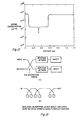
- a sample application example of the varactor controlled DIMPATT oscillator of the present invention is a phase-locked oscillator, which in essence is an amplifier with low noise figure, as shown in Figure 25.
- the frequency and the amplitude of the output power from the DIMPATT 402 is sampled through weak coupling 404.
- This video signal 408 is amplified and used to control the d.c. bias 410 of the varactor diode 412 until the DIMPATT frequency is locked onto f 1 .
- a second sampling of the output power can be fed to a detector 414 whose output voltage is proportional to rf voltage.
- This voltage is amplified and used to control d.c. bias current 416 which controls output (via comparator 418 and power supply 420 power of DIMPATT 402. Output power can be thus levelled to a desired value.
- the present invention provides a fundamental new innovation in monolithic microwave 'integrated circuits, and in solid state microwave and millimeter-wave components generally.
- An extremely broad scope of the equivalents of the present invention is therefore asserted, and the scope of the present invention is expressly not limited except as set forth in the accompanying Claims.
Landscapes
- Non-Reversible Transmitting Devices (AREA)
- Inductance-Capacitance Distribution Constants And Capacitance-Resistance Oscillators (AREA)
Applications Claiming Priority (4)
| Application Number | Priority Date | Filing Date | Title |
|---|---|---|---|
| US06/528,208 US4568889A (en) | 1983-08-31 | 1983-08-31 | Distributed diode VCO with stripline coupled output and distributed variable capacitor control |
| US528208 | 1983-08-31 | ||
| US06/528,210 US4525732A (en) | 1983-08-31 | 1983-08-31 | Distributed IMPATT structure |
| US528210 | 1990-05-24 |
Publications (2)
| Publication Number | Publication Date |
|---|---|
| EP0143887A2 true EP0143887A2 (de) | 1985-06-12 |
| EP0143887A3 EP0143887A3 (de) | 1987-05-20 |
Family
ID=27062648
Family Applications (1)
| Application Number | Title | Priority Date | Filing Date |
|---|---|---|---|
| EP84109043A Withdrawn EP0143887A3 (de) | 1983-08-31 | 1984-07-31 | Verbreiterte IMPATT Struktur |
Country Status (1)
| Country | Link |
|---|---|
| EP (1) | EP0143887A3 (de) |
Cited By (2)
| Publication number | Priority date | Publication date | Assignee | Title |
|---|---|---|---|---|
| DE3808251A1 (de) * | 1988-03-12 | 1989-09-21 | Licentia Gmbh | Halbleitersubstrat mit mindestens einem monolithisch integriertem schaltkreis |
| EP0367680A1 (de) * | 1988-11-04 | 1990-05-09 | Thomson-Csf | Monolitischer Halbleitermodul mit Lawinendiode und Anpassungsschaltungen für Hochfrequenzanwendungen und entsprechendes Verfahren zum Herstellen |
Family Cites Families (1)
| Publication number | Priority date | Publication date | Assignee | Title |
|---|---|---|---|---|
| GB1493602A (en) * | 1975-08-27 | 1977-11-30 | Secr Defence | Semiconductor devices |
-
1984
- 1984-07-31 EP EP84109043A patent/EP0143887A3/de not_active Withdrawn
Cited By (3)
| Publication number | Priority date | Publication date | Assignee | Title |
|---|---|---|---|---|
| DE3808251A1 (de) * | 1988-03-12 | 1989-09-21 | Licentia Gmbh | Halbleitersubstrat mit mindestens einem monolithisch integriertem schaltkreis |
| EP0367680A1 (de) * | 1988-11-04 | 1990-05-09 | Thomson-Csf | Monolitischer Halbleitermodul mit Lawinendiode und Anpassungsschaltungen für Hochfrequenzanwendungen und entsprechendes Verfahren zum Herstellen |
| FR2638897A1 (fr) * | 1988-11-04 | 1990-05-11 | Thomson Csf | Module semi-conducteur monolithique a diode a avalanche munie de circuits d'adaptation aux applications en hyperfrequence, et procede de fabrication correspondant |
Also Published As
| Publication number | Publication date |
|---|---|
| EP0143887A3 (de) | 1987-05-20 |
Similar Documents
| Publication | Publication Date | Title |
|---|---|---|
| US6362706B1 (en) | Cavity resonator for reducing phase noise of voltage controlled oscillator | |
| US3986153A (en) | Active millimeter-wave integrated circuit | |
| JP3175763B2 (ja) | マイクロ波発振器 | |
| US4568889A (en) | Distributed diode VCO with stripline coupled output and distributed variable capacitor control | |
| US7274263B2 (en) | Microstrip stabilized quantum well resonance-tunneling generator for millimeter and submillimeter wavelength range | |
| US6946934B2 (en) | Transmission line and semiconductor integrated circuit device | |
| US4131858A (en) | Beam lead dual parametric amplifier | |
| US4525732A (en) | Distributed IMPATT structure | |
| IL199490A (en) | A method and device for amplifying or creating a high frequency oscillation | |
| US4706041A (en) | Periodic negative resistance microwave structures and amplifier and oscillator embodiments thereof | |
| US4539528A (en) | Two-port amplifier | |
| Raisanen et al. | Subharmonic mixer with planar Schottky diodes in a novel split-block at 200-240 GHz | |
| Brehm et al. | Varactor-tuned integrated Gunn oscillators | |
| JP3610692B2 (ja) | 電圧制御発振器 | |
| Wanner et al. | Monolithically integrated SiGe push-push oscillators in the frequency range 50-190 GHz | |
| Hosoya et al. | RF HBT oscillators with low-phase noise and high-power performance utilizing a (/spl lambda//4/spl plusmn//spl delta/) open-stubs resonator | |
| US4380020A (en) | Active high frequency semiconductor device with integral waveguide | |
| Matsuzuka et al. | A 19 GHz low phase noise HFET VCO MMIC | |
| Singh | New developments in microwave devices and technology | |
| KR100675354B1 (ko) | 밀리미터 및 서브-밀리미터 파장용 전자기파를 생성하는양자 우물 공진 터널링 제너레이터를 안정화하는마이크로스트립 | |
| Stephan et al. | Lossy-line stabilization of negative-resistance diodes for integrated-circuit oscillators | |
| Zhou | A K-band Diffential-output GaAs pHEMT Voltage Controlled Oscillator | |
| Kelly et al. | A Low-Noise Millimeter MIC Mixer (Short Papers) | |
| Bogner et al. | 70 GHz planar integrated oscillator on semiinsulating GaAs | |
| Yasuda et al. | Quantum barrier varactor for coplanar waveguide applications |
Legal Events
| Date | Code | Title | Description |
|---|---|---|---|
| PUAI | Public reference made under article 153(3) epc to a published international application that has entered the european phase |
Free format text: ORIGINAL CODE: 0009012 |
|
| AK | Designated contracting states |
Designated state(s): DE FR GB NL |
|
| PUAL | Search report despatched |
Free format text: ORIGINAL CODE: 0009013 |
|
| AK | Designated contracting states |
Kind code of ref document: A3 Designated state(s): DE FR GB NL |
|
| 17P | Request for examination filed |
Effective date: 19871117 |
|
| 17Q | First examination report despatched |
Effective date: 19890913 |
|
| STAA | Information on the status of an ep patent application or granted ep patent |
Free format text: STATUS: THE APPLICATION IS DEEMED TO BE WITHDRAWN |
|
| 18D | Application deemed to be withdrawn |
Effective date: 19900424 |
|
| RIN1 | Information on inventor provided before grant (corrected) |
Inventor name: BAYRAKTAROGLU, BURHAN |