EP0367680A1 - Monolitischer Halbleitermodul mit Lawinendiode und Anpassungsschaltungen für Hochfrequenzanwendungen und entsprechendes Verfahren zum Herstellen - Google Patents
Monolitischer Halbleitermodul mit Lawinendiode und Anpassungsschaltungen für Hochfrequenzanwendungen und entsprechendes Verfahren zum Herstellen Download PDFInfo
- Publication number
- EP0367680A1 EP0367680A1 EP89403031A EP89403031A EP0367680A1 EP 0367680 A1 EP0367680 A1 EP 0367680A1 EP 89403031 A EP89403031 A EP 89403031A EP 89403031 A EP89403031 A EP 89403031A EP 0367680 A1 EP0367680 A1 EP 0367680A1
- Authority
- EP
- European Patent Office
- Prior art keywords
- mesa
- diode
- substrate
- forming
- avalanche
- Prior art date
- Legal status (The legal status is an assumption and is not a legal conclusion. Google has not performed a legal analysis and makes no representation as to the accuracy of the status listed.)
- Withdrawn
Links
Images



Classifications
-
- H—ELECTRICITY
- H10—SEMICONDUCTOR DEVICES; ELECTRIC SOLID-STATE DEVICES NOT OTHERWISE PROVIDED FOR
- H10W—GENERIC PACKAGES, INTERCONNECTIONS, CONNECTORS OR OTHER CONSTRUCTIONAL DETAILS OF DEVICES COVERED BY CLASS H10
- H10W44/00—Electrical arrangements for controlling or matching impedance
- H10W44/501—Inductive arrangements
-
- H—ELECTRICITY
- H10—SEMICONDUCTOR DEVICES; ELECTRIC SOLID-STATE DEVICES NOT OTHERWISE PROVIDED FOR
- H10N—ELECTRIC SOLID-STATE DEVICES NOT OTHERWISE PROVIDED FOR
- H10N89/00—Integrated devices, or assemblies of multiple devices, comprising at least one bulk negative resistance effect element covered by group H10N80/00
-
- H—ELECTRICITY
- H10—SEMICONDUCTOR DEVICES; ELECTRIC SOLID-STATE DEVICES NOT OTHERWISE PROVIDED FOR
- H10W—GENERIC PACKAGES, INTERCONNECTIONS, CONNECTORS OR OTHER CONSTRUCTIONAL DETAILS OF DEVICES COVERED BY CLASS H10
- H10W44/00—Electrical arrangements for controlling or matching impedance
- H10W44/20—Electrical arrangements for controlling or matching impedance at high-frequency [HF] or radio frequency [RF]
-
- H—ELECTRICITY
- H10—SEMICONDUCTOR DEVICES; ELECTRIC SOLID-STATE DEVICES NOT OTHERWISE PROVIDED FOR
- H10W—GENERIC PACKAGES, INTERCONNECTIONS, CONNECTORS OR OTHER CONSTRUCTIONAL DETAILS OF DEVICES COVERED BY CLASS H10
- H10W72/00—Interconnections or connectors in packages
-
- H—ELECTRICITY
- H10—SEMICONDUCTOR DEVICES; ELECTRIC SOLID-STATE DEVICES NOT OTHERWISE PROVIDED FOR
- H10W—GENERIC PACKAGES, INTERCONNECTIONS, CONNECTORS OR OTHER CONSTRUCTIONAL DETAILS OF DEVICES COVERED BY CLASS H10
- H10W90/00—Package configurations
Definitions
- the field of the invention is that of the generation and amplification of electromagnetic waves in the microwave band.
- the invention relates more precisely to the design and production, in the form of an integrated circuit of the monolithic type, of negative resistance elements of the IMPATT or GUNN diode type provided with circuits for adapting to microwave applications.
- the IMPATT or GUNN type diodes have a certain number of limitations, linked to their production technology, and to their impedance of use in microwave application.
- IMPATT diodes are available encapsulated in ceramic packages whose parasitic elements are located just at the level of the chip, without it being possible to modify their arrangement appreciably. This limits the operating frequency band, and imposes a relatively bulky coaxial propagation system.
- the impedance presented by the IMPATT or GUNN diodes is insufficient to allow direct adaptation to propagation lines of the type used in microstrip technology.
- Adaptation circuits are known which are designed to raise the output impedance of avalanche diodes.
- US patent 4,673,958 (BAYRAKTAROGLU) proposes such an adaptation circuit.
- the proposed solution shows the charge circuit the intrinsic negative resistance of the diode, of very low value.
- the electrical structure of the circuit does not allow to separate the frequency zone where we fight against the parasitic phenomena of the frequency zone where we exploit the negative resistance properties of the diode.
- the object of the invention is to overcome these various drawbacks.
- a first objective of the invention is to provide an avalanche diode component whose amplitude of the real term of the impedance presented at a microwave load is higher than for an avalanche diode alone.
- Another objective of the invention is to provide such a component which is directly usable in microstrip technology.
- An additional objective is to produce such a component which, compared to existing components compatible with coaxial or guided technology, provides the following advantages: - a decrease in weight and volume, - an improvement in electrical efficiency by reducing the lengths of the propagation line, - an increase in bandwidth by controlling the layout and the value of the elements located around the chip.
- the invention also aims to integrate the adaptation circuits into the components, which in particular makes it possible to use the principles of association of modules of the same type with a wider band. This extends the scope of negative resistance elements to agile radar transmitters and telecommunications amplifiers.
- an electronic circuit in particular intended for the generation and / or amplification of electromagnetic waves in the microwave range, of the type consisting of a negative resistance element such as an IMPATT or GUNN diode, to which a tuning inductor isolated from ground by a capacitor is connected in parallel, circuit characterized in that it is produced in the form of a monolithic semiconductor module comprising first and second mesas deposited on a highly thermally conductive layer, said first mesa constituting said negative resistance diode, and the second mesa forming said element insulation capacitive, and in that said mesas are connected by a metal blade in an air bridge, forming said tuning inductor.
- a monolithic semiconductor module comprising first and second mesas deposited on a highly thermally conductive layer, said first mesa constituting said negative resistance diode, and the second mesa forming said element insulation capacitive, and in that said mesas are connected by a metal blade in an air bridge, forming said tuning inductor.
- said mesa forming a capacitive element consists of a dielectric layer deposited between two metal layers.
- said mesa forming a capacitive element consists of a Schottky diode, intended to be reverse biased.
- said monolithic module comprises means for adapting to its impedance of use constituted by a third mesa forming adaptive capacity, and connected to said first mesa by a metal blade in bridge to air forming adaptation inductor.
- said third mesa is substantially of the same structure as said second mesa.
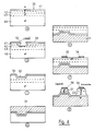
- the invention also relates to a method of manufacturing such a circuit, characterized in that it comprises the following steps: - An epitaxy is carried out on a semiconductor substrate, so as to reveal at least one avalanche zone, a transit zone, and a buffer layer; - A localized photoengraving of the substrate is carried out at the location of said second mesa; - said thermally conductive layer is deposited on contact said avalanche zone after metallization; - said first and second mesas are etched in said substrate, and their complementary constituent layers are deposited; - Depositing said metal bridge forming inductance of agreement, after thick resinating of the module, and opening of contacts at said mesas.
- said step of localized photogravure of the substrate consists in locally etching the avalanche and transit zones of said substrate, and said operation of depositing the constituent layers of the second mesa consists of depositing a dielectric material of the Si3N4 type.
- said localized photogravure step of the substrate consists in locally etching the avalanche zone of said substrate, and said operation of depositing the constituent layers of the second mesa consists in depositing a localized ohmic contact of the Au Ge Ni Ti Pt type At.
- the semiconductor material constituting the substrate is gallium arsenide.
- the embodiment described consists in integrating means of adaptation to an avalanche diode of the AsGa type, in the form of a semiconductor module.
- the electrical principle diagram of the chosen circuit proposed by M. HINES (Proceeding IEEEE vol. 60 Dec. 1972-p. 1544 fig. 6a) has interesting properties on two points: it presents variations, which in the zones [0 ; Fo / 2] and [Fa; Fc] are independent of each other making it easier to optimize the circuit. It increases, by a transformer effect, the negative real term seen by the charge circuit at Fo.
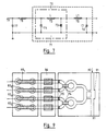
- This solution represented in FIG. 1, consists in putting in parallel on the IMPATT diode a tuning inductance Lc which is isolated from the ground by a capacitor Cp.
- the inductance is calculated so that the resonance with the dynamic capacitance Cd of the diode is at Fo. This then benefits from a step-up transformer effect of the intrinsic negative resistance of the diode.
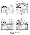
- a first version consists in making the insulation capacity Cp in the form of a dielectric capacitor (Fig. 2 and 4).
- the second version uses a Schottky diode for Cp (Fig 5 and 6).
- the module of this first version consists of 2 mesas 22, 23 deposited on a heat sink 21.
- the two mesas 22, 23 correspond respectively to a MIS (Metal Insulating Semi- conductor), and to an avalanche diode.
- the two mesas 22, 23 are connected to each other by a air bridge inductor 24.
- the layers N and N+ of the mesas 22, 23 come from a semiconductor substrate, of the type of Ga AS having undergone an epitaxy operation.
- the epitaxy performed on substrate N+ has the doping profile 40 seen in FIG. 3.
- - avalanche zone comprising a doping peak 44 located approximately 0.15 10 ⁇ 6 m deep
- - transit area 42
- - buffer layer 423
- border with the transit zone is located at a depth of approximately 3.10 ⁇ 6 m.
- this second version differs from the structure of Figure 2 in that the MIS capacity is replaced by a Schottky diode in charge of space, forming capacity.
- This Schottky diode is constituted by the mesa 51.
- a module can be produced in monolithic form including means for direct adaptation to the impedance of use.
- FIG. 7 The block diagram of this embodiment is presented in FIG. 7.
- the module 70 comprises the sub-module 71 with avalanche diode 72, tuning inductor 73 and insulation capacity 74, as described above.
- It also includes two adaptation elements 75, 76, corresponding respectively to an adaptation inductor 75, and to an adaptation capacity 76.
- All of these components 72, 73, 74, 75, 76 are integrated on the same monolithic module.
- the BF decoupling elements 77, 78 have been shown to illustrate a mode of use, with polarization 79.
- Figures 8a and 8b show an embodiment of such a module in side view ( Figure 8a) and in top view ( Figure 8b).
- the module consists of a main mesa 23 forming the avalanche diode, connected by two air bridge inductors 82, 83 to two side mesas 51, 81, substantially symmetrical. Each of these lateral mesas 51, 81 corresponds to a Schottky diode in charge of space, playing the role of capacitors 74 and 76.
- the association circuits are composed of a 3dB 91 coupler and two Wilkinson tees.
- the signal which arrives from the "input" gate 92 is also distributed in amplitude at the level of each module 931, 932, 933, 934.
- Balance charges 94 and series capacities 95 are arranged at the connections.
- the modules 93 are associated through a set of adaptation interfaces 96. Of course, it is possible to use adapted modules of the type of those of FIG. 8 in place of the pre-adapted modules 93, which avoids use interfaces 96.
- the signal synchronizes the modules on the same frequency and the synchronized signal is collected on the "output" gate 97, taking into account the well-known properties of the Wilkinson tees and the 3 dB coupler.
- the incident signal is reflected with amplification at the level of the modules and the amplified signal is collected on the "output" gate 93.
- the power levels reached are (15 W average, 60 W peak) in band I, (10 W average, 40 W peak) in band J
- the monolithic adapted or pre-adapted module can also be used in the transmission amplifiers described in French patent n ° 77.20657 by using propagation on microstrip on ceramic.
Landscapes
- Semiconductor Integrated Circuits (AREA)
- Electrodes Of Semiconductors (AREA)
Applications Claiming Priority (2)
| Application Number | Priority Date | Filing Date | Title |
|---|---|---|---|
| FR8814415A FR2638897B1 (fr) | 1988-11-04 | 1988-11-04 | Module semi-conducteur monolithique a diode a avalanche munie de circuits d'adaptation aux applications en hyperfrequence, et procede de fabrication correspondant |
| FR8814415 | 1988-11-04 |
Publications (1)
| Publication Number | Publication Date |
|---|---|
| EP0367680A1 true EP0367680A1 (de) | 1990-05-09 |
Family
ID=9371578
Family Applications (1)
| Application Number | Title | Priority Date | Filing Date |
|---|---|---|---|
| EP89403031A Withdrawn EP0367680A1 (de) | 1988-11-04 | 1989-11-03 | Monolitischer Halbleitermodul mit Lawinendiode und Anpassungsschaltungen für Hochfrequenzanwendungen und entsprechendes Verfahren zum Herstellen |
Country Status (2)
| Country | Link |
|---|---|
| EP (1) | EP0367680A1 (de) |
| FR (1) | FR2638897B1 (de) |
Cited By (3)
| Publication number | Priority date | Publication date | Assignee | Title |
|---|---|---|---|---|
| WO2007045232A3 (de) * | 2005-10-21 | 2007-06-21 | Fraunhofer Gesellchaft Zur Foe | Photodioden-chip hoher grenzfrequenz |
| US8034666B2 (en) | 2009-11-15 | 2011-10-11 | Microsemi Corporation | Multi-layer thick-film RF package |
| US8410601B2 (en) | 2009-11-15 | 2013-04-02 | Microsemi Corporation | RF package |
Citations (5)
| Publication number | Priority date | Publication date | Assignee | Title |
|---|---|---|---|---|
| DE2001468A1 (de) * | 1970-01-14 | 1971-07-22 | Philips Nv | Verfahren zur Herstellung von Halbleiterbauelementen |
| US4436766A (en) * | 1981-05-15 | 1984-03-13 | The United States Of America As Represented By The Secretary Of The Navy | Plated bridge step-over connection for monolithic devices and method for making thereof |
| EP0143887A2 (de) * | 1983-08-31 | 1985-06-12 | Texas Instruments Incorporated | Verbreiterte IMPATT Struktur |
| EP0222203A1 (de) * | 1985-11-15 | 1987-05-20 | BBC Brown Boveri AG | Leistungshalbleitermodul |
| US4673958A (en) * | 1985-01-31 | 1987-06-16 | Texas Instruments Incorporated | Monolithic microwave diodes |
-
1988
- 1988-11-04 FR FR8814415A patent/FR2638897B1/fr not_active Expired - Lifetime
-
1989
- 1989-11-03 EP EP89403031A patent/EP0367680A1/de not_active Withdrawn
Patent Citations (5)
| Publication number | Priority date | Publication date | Assignee | Title |
|---|---|---|---|---|
| DE2001468A1 (de) * | 1970-01-14 | 1971-07-22 | Philips Nv | Verfahren zur Herstellung von Halbleiterbauelementen |
| US4436766A (en) * | 1981-05-15 | 1984-03-13 | The United States Of America As Represented By The Secretary Of The Navy | Plated bridge step-over connection for monolithic devices and method for making thereof |
| EP0143887A2 (de) * | 1983-08-31 | 1985-06-12 | Texas Instruments Incorporated | Verbreiterte IMPATT Struktur |
| US4673958A (en) * | 1985-01-31 | 1987-06-16 | Texas Instruments Incorporated | Monolithic microwave diodes |
| EP0222203A1 (de) * | 1985-11-15 | 1987-05-20 | BBC Brown Boveri AG | Leistungshalbleitermodul |
Non-Patent Citations (1)
| Title |
|---|
| PROCEEDINGS OF THE GALLIUM ARSENIDE INTEGRATED CIRCUIT SYMPOSIUM, New Orleans, 9-11 novembre 1982, pages 25-28, IEEE, New York, US; G.D. McCORMACK et al.: "A GaAs MSI 8-bit multiplexer and demultiplexer" * |
Cited By (5)
| Publication number | Priority date | Publication date | Assignee | Title |
|---|---|---|---|---|
| WO2007045232A3 (de) * | 2005-10-21 | 2007-06-21 | Fraunhofer Gesellchaft Zur Foe | Photodioden-chip hoher grenzfrequenz |
| EP2323177A1 (de) * | 2005-10-21 | 2011-05-18 | Fraunhofer Gesellschaft zur Förderung der angewandten Wissenschaft E.V. | Photodioden-Chip hoher Grenzfrequenz |
| US8044481B2 (en) | 2005-10-21 | 2011-10-25 | Fraunhofer-Gesellschaft Zur Foderung Der Angewandten Forschung E.V. | Photodiode chip having a high limit frequency |
| US8034666B2 (en) | 2009-11-15 | 2011-10-11 | Microsemi Corporation | Multi-layer thick-film RF package |
| US8410601B2 (en) | 2009-11-15 | 2013-04-02 | Microsemi Corporation | RF package |
Also Published As
| Publication number | Publication date |
|---|---|
| FR2638897A1 (fr) | 1990-05-11 |
| FR2638897B1 (fr) | 1992-08-07 |
Similar Documents
| Publication | Publication Date | Title |
|---|---|---|
| FR2652197A1 (fr) | Transformateurs du type symetrique-dissymetrique perfectionnes. | |
| FR2916108A1 (fr) | Amplificateur de puissance a haute frequence | |
| US4673958A (en) | Monolithic microwave diodes | |
| EP1312116A1 (de) | Verteiltes abschirmungs- und/oder entkopplungsverfahren für vorrichtung mit dreidimensionaler verdrahtungsstruktur | |
| FR3119269A1 (fr) | Impression par transfert pour applications RF | |
| EP1535346A2 (de) | Quasi-vertikales leistungshalbleiterbauelement auf einem verbindungssubstrat | |
| EP0161166B1 (de) | Kompakter Addierer mit Halbleiteranordnungen im Hyperfrequenz-Betrieb | |
| FR2597678A1 (fr) | Oscillateur commande par une tension, doubleur de frequence. | |
| EP0149390A2 (de) | Feldeffekttransistor mit vertikaler Sub-Mikronstruktur und Verfahren zu dessen Herstellung | |
| EP0446108A1 (de) | Dielektrischer Resonator mit Mikrowellenmetallstreifen und mit diesem Resonator ausgerüstete Vorrichtung | |
| EP0133101A1 (de) | Verbindungsanordnung für die Zelle einer vorimplantierten integrierten Hyperfrequenzschaltung | |
| FR2638897A1 (fr) | Module semi-conducteur monolithique a diode a avalanche munie de circuits d'adaptation aux applications en hyperfrequence, et procede de fabrication correspondant | |
| FR2878081A1 (fr) | Procede de realisation d'antennes integrees sur puce ayant une efficacite de rayonnement ameliore. | |
| EP0158550B1 (de) | Hyperfrequenz-Halbleiteranordnung mit äusseren Balkenleiter-Verbindungen | |
| EP0109899B1 (de) | Präangepasster Modul für Hyperfrequenz-Diode mit hoher Wärmeabfuhr | |
| EP0684653A1 (de) | Lichtgesteuerter Heterostruktur-Halbleiterbaustein zur Erzeugung von Höchstfrequenz-Schwingungen | |
| EP0204387B1 (de) | Halbleiteranordnung zur Herstellung der Entkupplungskapazitäten, die zwischen der Versorgung und der Erdung von integrierten Schaltungen liegen | |
| EP0969509A1 (de) | Monolithische integrierte Schaltung mit einer flachen Induktanz oder einem flachen Transformator, und Herstellungsverfahren einer solchen Schaltung | |
| EP0156708B1 (de) | Hyperfrequenztransistoroszillator gesteuert durch eine Kapazitätsdiode | |
| EP3262707A1 (de) | Dreidimensionale elektrische lc-resonatorvorrichtung | |
| FR2536211A1 (fr) | Structure de diode hyperfrequences dont les connexions exterieures sont prises par deux poutres metalliques | |
| Nafra et al. | Indirect optical control of microwave circuits using monolithic optically variable capacitors | |
| EP0420106B1 (de) | Attenuatorschaltung mit einem Dual-Gate-Feldeffekttransistor | |
| EP0017562B1 (de) | Festkörper-Mikrowellenquelle | |
| FR2792775A1 (fr) | Dispositif de circuit integre comprenant une inductance a haut coefficient de qualite |
Legal Events
| Date | Code | Title | Description |
|---|---|---|---|
| PUAI | Public reference made under article 153(3) epc to a published international application that has entered the european phase |
Free format text: ORIGINAL CODE: 0009012 |
|
| AK | Designated contracting states |
Kind code of ref document: A1 Designated state(s): DE GB IT NL |
|
| STAA | Information on the status of an ep patent application or granted ep patent |
Free format text: STATUS: THE APPLICATION IS DEEMED TO BE WITHDRAWN |
|
| 18D | Application deemed to be withdrawn |
Effective date: 19901110 |