EP0143912A2 - Codeur pour code HDB3 à deux niveaux - Google Patents
Codeur pour code HDB3 à deux niveaux Download PDFInfo
- Publication number
- EP0143912A2 EP0143912A2 EP84110524A EP84110524A EP0143912A2 EP 0143912 A2 EP0143912 A2 EP 0143912A2 EP 84110524 A EP84110524 A EP 84110524A EP 84110524 A EP84110524 A EP 84110524A EP 0143912 A2 EP0143912 A2 EP 0143912A2
- Authority
- EP
- European Patent Office
- Prior art keywords
- gate
- regenerator
- output
- interface
- input
- Prior art date
- Legal status (The legal status is an assumption and is not a legal conclusion. Google has not performed a legal analysis and makes no representation as to the accuracy of the status listed.)
- Withdrawn
Links
- 230000005540 biological transmission Effects 0.000 abstract description 9
- 230000003287 optical effect Effects 0.000 abstract 1
- 102100029469 WD repeat and HMG-box DNA-binding protein 1 Human genes 0.000 description 4
- 101710097421 WD repeat and HMG-box DNA-binding protein 1 Proteins 0.000 description 4
- 238000006243 chemical reaction Methods 0.000 description 4
- 238000010586 diagram Methods 0.000 description 3
- 239000013307 optical fiber Substances 0.000 description 3
- 238000001208 nuclear magnetic resonance pulse sequence Methods 0.000 description 2
- 241001547070 Eriodes Species 0.000 description 1
- 230000015572 biosynthetic process Effects 0.000 description 1
- 230000008676 import Effects 0.000 description 1
- 230000000737 periodic effect Effects 0.000 description 1
- 230000007704 transition Effects 0.000 description 1
Images

Classifications
-
- H—ELECTRICITY
- H04—ELECTRIC COMMUNICATION TECHNIQUE
- H04L—TRANSMISSION OF DIGITAL INFORMATION, e.g. TELEGRAPHIC COMMUNICATION
- H04L25/00—Baseband systems
- H04L25/38—Synchronous or start-stop systems, e.g. for Baudot code
- H04L25/40—Transmitting circuits; Receiving circuits
- H04L25/49—Transmitting circuits; Receiving circuits using code conversion at the transmitter; using predistortion; using insertion of idle bits for obtaining a desired frequency spectrum; using three or more amplitude levels ; Baseband coding techniques specific to data transmission systems
- H04L25/4906—Transmitting circuits; Receiving circuits using code conversion at the transmitter; using predistortion; using insertion of idle bits for obtaining a desired frequency spectrum; using three or more amplitude levels ; Baseband coding techniques specific to data transmission systems using binary codes
- H04L25/4908—Transmitting circuits; Receiving circuits using code conversion at the transmitter; using predistortion; using insertion of idle bits for obtaining a desired frequency spectrum; using three or more amplitude levels ; Baseband coding techniques specific to data transmission systems using binary codes using mBnB codes
- H04L25/491—Transmitting circuits; Receiving circuits using code conversion at the transmitter; using predistortion; using insertion of idle bits for obtaining a desired frequency spectrum; using three or more amplitude levels ; Baseband coding techniques specific to data transmission systems using binary codes using mBnB codes using 1B2B codes
- H04L25/4912—Transmitting circuits; Receiving circuits using code conversion at the transmitter; using predistortion; using insertion of idle bits for obtaining a desired frequency spectrum; using three or more amplitude levels ; Baseband coding techniques specific to data transmission systems using binary codes using mBnB codes using 1B2B codes using CMI or 2-HDB-3 code
Definitions
- the invention relates to an encoder for the generation of signals in the two-level HDB3 code for connection to outputs of an interface regenerator, with the clock output and one of two regenerator outputs for the regenerated pulses of one polarity, the inputs of an AND gate are connected.
- interface codes are defined depending on the hierarchy level for the connecting lines between digital transmission devices.
- Pseudo-ternary interface codes are defined for all bit rates from 34 kbit / s to 45 Mbit / s listed in the recommendation.
- these codes each with three amplitude levels, are not particularly suitable for transmission via optical fibers.
- the transmission of digital signals via optical fibers is usually carried out using a two-stage transmission code.
- binary block codes mBnB are used, in which blocks with m binary characters are converted into blocks with a larger number n binary characters. A block synchronization is required for the conversion back on the receiving side, which is generally not possible for every periodic binary input signal pattern.
- a line terminal therefore has the chain connection of a converter from the interface in addition to the interface regenerator code into the binary code, a scrambler and a recoder from the binary code into the actual transmission code, a binary block code.
- a so-called two-level HDB3 coder with a coder and a decoder is known from the technical notices PTT 7/1979, pages 253 to 266, in particular from pages 256 to 258.
- the formation law for the code mentioned is that every positive one state in the HDB3 code with NRZ format is converted into a bit half combination "11", that every negative one state in the HDB3 code is converted into a bit half combination "00" and that every zero state in HDB3 encoder is converted into either the bit-half combination "01” or the bit-half combination "10".
- the object of the present invention is therefore to provide an encoder of the type mentioned at the outset, which is as inexpensive as possible.
- an AND gate is provided with at least three inputs, at least two of which are inverting, that two inverting inputs are separately connected to the regenerator outputs, that the output of the AND gate is connected to a first input of an OR -Gatters is connected, the output of which represents the encoder output, that a second input of the OR gate either with either the regenerator output for the positive regenerated pulses and the clock output of the interface regenerator a third inverting input of the AND gate is connected or that the second input of the OR gate is connected to the regenerator output for the negative regenerated pulses and for this purpose the clock output of the interface regenerator is connected to a third, non-inverting input of the OR gate.
- the encoder therefore only requires the additional use of an AND gate and an OR gate, and when the OR gate is implemented as a so-called wired OR gate, the encoder practically only requires a single gate and, in addition to low expenditure and low current consumption, also via one has high transmission speed.
- the possibility of generating signals in the HDBn, CHDBn and BnZS codes with the encoder according to the invention is also of essential importance.
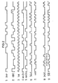
- the interface regenerator SR represents a conventional PCM regenerator, which regenerates the pseudoternary signals received at the input E in terms of amplitude and time, and thereby converts the pseudoternary signals into two unipolar pulse trains, the one pulse train being emitted, for example, via line 4 from the interface regenerator output , the positive input signal pulses and the second unipolar pulse train via line 5 the negative input im pulse of the pseudo ternary signal corresponds.
- Both import p ul sans be delivered to inverting inputs of a downstream AND gate AND1, AND2.
- the output of the AND gate is connected downstream in each case to one input of OR gate OR t eten connected.
- This OR gate is shown with regard to its function, but in practice it is implemented by a so-called wired OR gate, so that the encoder according to the invention is limited to an AND gate with three inputs.
- the other input of the OR gate is connected to one of the two Regeneratorauserie comparable b reasons, where a pulse of the regenerated signal is present.
- a further inverting input is provided as the third input of the AND gate AND1 and is connected to the clock output of the interface regenerator SR.
- the clock output of this regenerator is connected to a non-inverting input of the AND gate AND2 in accordance with FIG. 1b.
- Line 2 shows the corresponding HDB3-coded signal, which is fed to the input E of the interface regenerator SR in the form, if necessary, through the transmission.
- the clock generated in Thomasstellenregenerator is shown with a T akt p eriode the symbol duration of the binary or the HDB3 code corresponds.
- Line 4 shows the pulses occurring at output 4 of the interface regenerator, which result in a unipolar pulse train and represent the positive pulses of the input signal according to line 2. Ent In line 5, the pulses occurring at output 5 of the interface regenerator are correspondingly shown, which correspond to the negative input pulses.
- Line 8 shows the pulses occurring at the output 8 of the second AND gate AND2, which result in the second AND gate from the inverted signals at the outputs 4 and 5 of the interface regenerator and the non-inverted clock signal from the output 3.
Landscapes
- Physics & Mathematics (AREA)
- Spectroscopy & Molecular Physics (AREA)
- Engineering & Computer Science (AREA)
- Computer Networks & Wireless Communication (AREA)
- Signal Processing (AREA)
- Dc Digital Transmission (AREA)
- Communication Control (AREA)
Applications Claiming Priority (2)
| Application Number | Priority Date | Filing Date | Title |
|---|---|---|---|
| DE3332285 | 1983-09-07 | ||
| DE19833332285 DE3332285A1 (de) | 1983-09-07 | 1983-09-07 | Codierer fuer den zweipegel-hdb3-code |
Publications (2)
| Publication Number | Publication Date |
|---|---|
| EP0143912A2 true EP0143912A2 (fr) | 1985-06-12 |
| EP0143912A3 EP0143912A3 (fr) | 1988-03-23 |
Family
ID=6208472
Family Applications (1)
| Application Number | Title | Priority Date | Filing Date |
|---|---|---|---|
| EP84110524A Withdrawn EP0143912A3 (fr) | 1983-09-07 | 1984-09-04 | Codeur pour code HDB3 à deux niveaux |
Country Status (2)
| Country | Link |
|---|---|
| EP (1) | EP0143912A3 (fr) |
| DE (1) | DE3332285A1 (fr) |
-
1983
- 1983-09-07 DE DE19833332285 patent/DE3332285A1/de not_active Withdrawn
-
1984
- 1984-09-04 EP EP84110524A patent/EP0143912A3/fr not_active Withdrawn
Non-Patent Citations (1)
| Title |
|---|
| BULLETIN TECHNIQUE PTT, TECHNISCHE MITTEILUNGEN der PTT, Nr. 7, 1979, Seiten 253-266; C. BEGUIN: "Digitales Lichtwellenleiter-Versuchssystem f}r 8,448 Mbit/s" * |
Also Published As
| Publication number | Publication date |
|---|---|
| EP0143912A3 (fr) | 1988-03-23 |
| DE3332285A1 (de) | 1985-03-21 |
Similar Documents
| Publication | Publication Date | Title |
|---|---|---|
| DE2944459C2 (de) | Verfahren zum Übertragen von Bipolarsignalen mittels eines optischen Senders | |
| DE2656054A1 (de) | Vorrichtung zur wortsynchronisation in einer optischen nachrichtenanlage | |
| DE2712974C2 (de) | Schaltungsanordnung zum Erzeugen von Signalen im Code-Mark-Inversion - Code | |
| DE3000941C2 (de) | Anordnung zur Übertragung zusätzlicher Informationen für eine Einrichtung zur Übertragung digitaler Daten | |
| EP0111309B1 (fr) | Décodeur CMI | |
| DE3031579C2 (de) | CMI-Codierer | |
| EP0097947B1 (fr) | Dispositif pour générer des séquences pseudo-aléatoires en code AMI | |
| DE3828864C2 (fr) | ||
| DE4223639C1 (de) | Verfahren zum Übertragen zweier voneinander unabhängiger digitaler Signale | |
| DE2850129A1 (de) | Schaltungsanordnung zur umwandlung von binaeren digitalsignalen in pseudoternaere wechselimpulse | |
| EP0143912A2 (fr) | Codeur pour code HDB3 à deux niveaux | |
| EP0136663A2 (fr) | Système de transmission de signaux codés d'après la loi AMI | |
| DE2649161C3 (de) | Digitales Übertragungssystem mit einem Alphabet-Code-Wandler | |
| DE2852374C2 (de) | Verfahren und Schaltungsanordnung zur frequenzmodulierten Übertragung eines Binärsignals | |
| DE2430760A1 (de) | Hdb3-codec | |
| DE3107602A1 (de) | Verfahren zur codierung von analogsignalen | |
| EP0197475B1 (fr) | Brouilleur et débrouilleur multiplicatif opérant par mots | |
| DE2755522C3 (de) | Frequenzverschiebung des Hauptenergiebereichs eines pseudoternär codierten digitalen Signals | |
| DE3117221A1 (de) | Umsetzung von binaeren signalen fuer lichtwellenleiteruebertragungssysteme | |
| EP0250729B1 (fr) | Appareil pour transmettre une suite de données | |
| DE1537016B2 (de) | Verfahren und schaltungsanordnung zur uebertragung von binaeren eingangsdaten mittels einer modifizierten duobinae ren traegermodulation | |
| DE2543428A1 (de) | Verfahren und anordnung zur uebertragung von binaer-informationen | |
| DE4234628C1 (de) | Codewandler zur Erzeugung eines duobinären Codes | |
| EP0556697B1 (fr) | Méthode et dispositif de transmission d'information auxiliaire | |
| DE2748154A1 (de) | Datenuebertragungssystem mit pulslagemodulation |
Legal Events
| Date | Code | Title | Description |
|---|---|---|---|
| PUAI | Public reference made under article 153(3) epc to a published international application that has entered the european phase |
Free format text: ORIGINAL CODE: 0009012 |
|
| AK | Designated contracting states |
Designated state(s): AT BE CH DE FR GB IT LI NL SE |
|
| PUAL | Search report despatched |
Free format text: ORIGINAL CODE: 0009013 |
|
| AK | Designated contracting states |
Kind code of ref document: A3 Designated state(s): AT BE CH DE FR GB IT LI NL SE |
|
| STAA | Information on the status of an ep patent application or granted ep patent |
Free format text: STATUS: THE APPLICATION IS DEEMED TO BE WITHDRAWN |
|
| 18D | Application deemed to be withdrawn |
Effective date: 19880924 |
|
| RIN1 | Information on inventor provided before grant (corrected) |
Inventor name: POSPISCHIL, REGINHARD, DR. DIPL.-ING. |