EP0144647A1 - Amplificateur différentiel - Google Patents
Amplificateur différentiel Download PDFInfo
- Publication number
- EP0144647A1 EP0144647A1 EP84112524A EP84112524A EP0144647A1 EP 0144647 A1 EP0144647 A1 EP 0144647A1 EP 84112524 A EP84112524 A EP 84112524A EP 84112524 A EP84112524 A EP 84112524A EP 0144647 A1 EP0144647 A1 EP 0144647A1
- Authority
- EP
- European Patent Office
- Prior art keywords
- transistors
- differential amplifier
- transistor
- voltage
- collectors
- Prior art date
- Legal status (The legal status is an assumption and is not a legal conclusion. Google has not performed a legal analysis and makes no representation as to the accuracy of the status listed.)
- Granted
Links
- 230000000295 complement effect Effects 0.000 claims description 3
- 230000003321 amplification Effects 0.000 description 7
- 238000003199 nucleic acid amplification method Methods 0.000 description 7
- 238000010586 diagram Methods 0.000 description 5
- 230000000694 effects Effects 0.000 description 2
- 238000004519 manufacturing process Methods 0.000 description 2
- 230000003247 decreasing effect Effects 0.000 description 1
- 230000003068 static effect Effects 0.000 description 1
Images

Classifications
-
- H—ELECTRICITY
- H03—ELECTRONIC CIRCUITRY
- H03F—AMPLIFIERS
- H03F3/00—Amplifiers with only discharge tubes or only semiconductor devices as amplifying elements
- H03F3/30—Single-ended push-pull [SEPP] amplifiers; Phase-splitters therefor
-
- H—ELECTRICITY
- H03—ELECTRONIC CIRCUITRY
- H03F—AMPLIFIERS
- H03F1/00—Details of amplifiers with only discharge tubes, only semiconductor devices or only unspecified devices as amplifying elements
- H03F1/08—Modifications of amplifiers to reduce detrimental influences of internal impedances of amplifying elements
- H03F1/22—Modifications of amplifiers to reduce detrimental influences of internal impedances of amplifying elements by use of cascode coupling, i.e. earthed cathode or emitter stage followed by earthed grid or base stage respectively
-
- H—ELECTRICITY
- H03—ELECTRONIC CIRCUITRY
- H03F—AMPLIFIERS
- H03F3/00—Amplifiers with only discharge tubes or only semiconductor devices as amplifying elements
- H03F3/45—Differential amplifiers
- H03F3/45071—Differential amplifiers with semiconductor devices only
- H03F3/45076—Differential amplifiers with semiconductor devices only characterised by the way of implementation of the active amplifying circuit in the differential amplifier
- H03F3/4508—Differential amplifiers with semiconductor devices only characterised by the way of implementation of the active amplifying circuit in the differential amplifier using bipolar transistors as the active amplifying circuit
- H03F3/45085—Long tailed pairs
- H03F3/45094—Folded cascode stages
Definitions
- the present invention relates to a differential amplifier and, more particularly, to a high-speed wide-band differential amplifier.
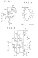
- Fig. 1 shows a conventional differential amplifier.
- This differential amplifier has npn transistors Ql and Q2 as a differential pair.
- the bases of the npn transistors Ql and Q2 are connected to input terminals 10 and 12, respectively.
- the emitter of the npn transistor Ql is connected to the emitter of the npn transistor Q2 through resistors Rl and R2.
- the junction between the resistors Rl and R 2 is grounded through a constant current source CS.
- the collectors of the npn transistors Ql and Q2 are connected to the emitters of other npn transistors Q3 and Q4, respectively.
- the bases of the npn transistors Q3 and Q4 are commonly connected to a bias voltage source 16.
- the collectors of the npn transistors Q3 and Q4 are connected to output terminals 18 and 20, respectively. These collectors are also connected to a power source terminal 22 through resistors R3 and R4, respectively.
- the differential amplifier shown in Fig. 1 generates an output signal SO from the output terminals 18 and 20 in accordance with an input signal SI.
- the input signal SI represents the difference between voltages applied to the input terminals 10 and 12.
- Fig. 2 shows the relationship between the power source voltage and the input and output signals SI and SO with respect to the differential amplifier.
- V denotes the maximum voltage of the input signal SI
- VI1 denotes a voltage amplitude between the maximum and minimum voltages of the input signal SI
- VOl denotes a voltage amplitude between the maximum and minimum voltages of the output signal SO
- VCC denotes the potential at a power source terminal 22
- VB denotes the output voltage from the bias voltage source 16
- VBE denotes the voltage between the base and emitter of the transistors Q3 and Q4
- different voltage ranges are assigned to voltage variations of the input signal SI and the output signal SO. The following condition is required in order not to saturate the transistors Ql and Q2 in the amplification of the input signal SI:
- the voltage amplitude VOl of the output signal SO must be limited to a small value.
- the margin for fluctuation of the power source voltage VCC is small. It is therefore very difficult to maintain a predetermined dynamic range.
- the power source voltage VCC is set at a low value, the reliability of this differential amplifier becomes low.
- the voltage amplitude VII of the input signal SI is large, the high-frequency amplification characteristics of this differential amplifier are degraded by a Miller effect due to capacitances between collectors and bases of the transistors Ql and Q2. In this case, the differential amplifier cannot linearly amplify the input signal SI in a wide frequency range.
- Fig. 3 shows an improved conventional differential amplifier.
- This differential amplifier has npn transistors Ql and Q2 as a differential pair and pnp transistors Q5 and Q6 as another differential pair.
- the bases of the transistors Ql and Q5 are commonly connected to a first input terminal 10, and the bases of the transistors Q2 and Q6 are commonly connected to a second input terminal 12.
- the input signal SI is supplied across the first and second input terminals 10 and 12.
- the emitter of the transistor Ql is connected to the emitter of the transistor Q2 through resistors Rl and R2.
- the junction between the resistors Rl and R2 is grounded through a constant current source CS2.
- the emitter of the transistor Q5 is connected to the emitter of the transistor Q6 through resistors R5 and R6.
- the junction between the resistors R5 and R6 . is connected to a power source terminal 22 through a constant current source CS1.
- the collector of the transistor Ql is connected to the power source terminal 22, and the collector of the transistor Q5 is grounded.
- the collector of the npn transistor Q2 is connected to the emitter of the pnp transistor Q7.
- the base of the transistor Q7 is connected to a first bias voltage source 24, and the emitter thereof is connected to the power source terminal 22 through a resistor R7.
- the collector of the npn transistor Q6 is connected to the emitter of the npn transistor Q8.
- the base of the transistor Q8 is connected to the second bias voltage source 26.
- the emitter of the transistor Q8 is grounded through a resistor R8.
- the collectors of the transistors Q7 and Q8 are commonly connected to the output terminal 18.
- the resistor R9 is connected across the output terminals 18 and 20.
- the output terminal 20 is grounded.
- the input signal SI when the input signal SI is supplied across the input terminals 10 and 12, the input signal SI is supplied to the differential pair of the transistors Ql and Q2 and the differential pair of the transistors Q5 and Q6.
- the transistors Q5 and Q6 generate an output signal having an opposite phase to that of the output signal from the transistors Ql and Q2. Therefore, the dynamic range of the collector currents of the transistors Q7 and Q8 can be widened. In this case, in order not to generate an offset voltage at the output terminals of the differential amplifier shown in Fig. 3, the amplification characteristics of the differential pairs must be the same.
- the differential amplifier shown in Fig. 3 requires a number of circuit elements, resulting in a high manufacturing cost.
- a differential amplifier comprising: first and second input terminals for receiving first and second voltage signals; a detecting circuit for detecting the voltage difference between the first and second voltage signals, the detecting circuit including first and second transistors whose bases are respectively connected to the first and second input terminals and a constant current source connected to the emitters of the first and second transistors; a current supplying circuit having first and second terminals respectively connected to the collectors of the first and second transistors, and for supplying constant currents from said first and second terminals; and an amplifying circuit including third and fourth transistors whose emitters respectively are connected to the first and second terminals of the current supplying circuit and which have a complementary relationship with the respective first and second transistors, a bias circuit for supplying bias voltages to the bases of the third and fourth transistors, and a load circuit connected between the collectors of the third and fourth transistors and the ground.
- differential amplifier of the present invention a wide dynamic range can be guaranteed at a relatively low power source voltage.
- This differential amplifier amplifies an input signal at a wide range and at a high speed, thereby providing a wide variety of applications of this differential amplifier.
- a differential amplifier according to an embodiment of the present invention will be described with reference to Figs. 4 and 5.
- This differential amplifier has npn transistors Q10 and Q12 as a differential pair.
- the bases of the npn transistors Q10 and Q12 are connected to input terminals 30 and 32, respectively.
- the emitter of the npn transistor Q10 is connected to the emitter of the npn transistor Q12 through resistors R10 and R12 in series..
- the junction between the resistors R10 and R12 is connected to a reference potential terminal VEE, e.g., the ground through a constant current source CS.
- An input signal SI in Fig. 4 corresponds to a voltage difference between a first voltage applied to the input terminal 30 and a second voltage applied to the input terminal 32.
- the differential amplifier further comprises pnp transistors Q14 and Q16.
- the pnp transistors Q14 and Q16 are complementary with the npn transistors Q10 and Q12, respectively.
- the emitter of the pnp transistor Q14 is connected to the collector of the npn transistor Q10 and to a power source terminal 34 through a resistor R14.
- the emitter of the pnp transistor Q16 is connected to the collector of the npn transistor Q12 and to a power source terminal 34 through a resistor R16.
- the power source terminal 34 is set at a VCC level potential.
- the collector of the pnp transistor Q14 is connected to the output terminal 36 and is grounded through a resistor R18.
- the collector of the pnp transistor Q16 is connected to the output terminal 38 and is grounded through a resistor R20.
- the difference between voltage drops across the resistors R18 and R20 is supplied as an output signal SO across the output terminals 36 and 38.
- the bases of the pnp transistors Q14 and Q16 are commonly connected to a bias voltage source 40.
- the resistors RIO, R14 and R18 have the same resistances as the resistors R12, R16 and R20, respectively.
- the npn and pnp transistors Q10 and Q14 have the same static characteristics as the npn and pnp transistors Q12 and Q16, respectively.
- a collector current through the transistor Q10 is larger than that through the npn transistor Q12.
- the currents flowing through the load resistors R14 and R16 of the npn transistors Q10 and Q12 will not be changed and are kept constant. Therefore, the collector current through the pnp transistor Q14 changes at a smaller amplitude than that of the collector current flowing through the pnp transistor Q16. In this case, the voltage drop across the resistor R18 is smaller than that across the resistor R20. As a result, a positive voltage appears as the output signal SO across the output terminals 36 and 38.
- the collector current through the npn transistor Q12 is larger than that through the npn transistor Q10.
- a collector current through the pnp transistor Q16 changes at a smaller amplitude than that of the collector current flowing through the pnp transistor Q14.
- a voltage drop across the load resistor R18 is smaller than that across the load resistor R20.
- a negative voltage appears as the output signal SO across the output terminals 36 and 38.
- the differential amplifier generates the output signal SO having the same phase as the input signal SI.
- the output signal SO is amplified to have a larger amplitude than that of the input signal SI by means of a first common-base amplifier constituted by the pnp transistor Q14 and the resistor R18 and a second common-base amplifier constituted by the pnp transistor Q16 and the resistor R20.
- Fig. 5 is the power source voltage and a chart explaining the relationship between the input and output signals with respect to this differential amplifier.
- VP2 denotes a maximum voltage of the input signal SI
- VI2 denotes a voltage amplitude between the maximum and minimum voltages of the input signal SI
- V02 denotes a voltage amplitude between the maximum and minimum voltages of the output signal SO
- VBE denotes the voltage between the base and emitter of the npn transistors Q10 and Q12
- VB denotes the output voltage from the bias voltage source 40.
- the input signal SI and the output signal SO change between the power source voltage VCC and ground.
- a specific voltage range is commonly used for the input and output signals SI and SO.
- the bias voltage VB is adjusted to come closer to the power source voltage VCC so as to set the VP2 in equation (3) and V02 in relation (4) to be larger than VP1 and V01, thereby widening the dynamic range of the differential amplifier.
- the dynamic range is predetermined, a fluctuation margin of the power source voltage VCC which is allowed for the predetermined dynamic range can be set to be large in this differential amplifier. For this reason, even if the power source voltage is set at a relatively low value, the operation of the differential amplifier can be guaranteed.
- the collectors of the npn transistors Q10 and Q12 are connected to the emitters of the transistors Q14 and Q16 in the common-base configuration, and a current flows from the power source terminal 34 into the emitters of pnp transistors Q14, Q16 through the resistors R14, R16.
- the constant current source CS is set to supply a constant current lower than a constant current flowing into the resistors R14, R16.
- the output inpedance of the npn transistors Q10, Q12 is kept low. For this reason, the Miller effect caused by capacitances between the collectors and bases of the npn transistors Q10 and Q12 will not appear even if the input signal SI has a large amplitude.
- this differential amplifier has a wide-range amplification and fast response-time characteristics.
- the number of circuit elements in this differential amplifier is smaller than that of the differential amplifier in Fig. 3. Therefore, it is very easy to match the npn transistors Q10 and Q12, and the pnp transistors Q14 and Q16, thereby decreasing the manufacturing cost of the differential amplifier.
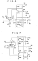
- Fig. 6 shows a differential amplifier wherein the active loads are constituted by a current mirror circuit.
- a current mirror circuit 50 comprises npn transistors Q18 and Q20.
- the base of the npn transistor Q18 is connected to its collector and to the base of the npn transistor Q20.
- the collectors of the npn transistors Q18 and'Q20 are connected to the collectors of the pnp transistors Q14 and Q16, respectively.
- the emitters of the npn transistors Q18 and Q20 are grounded through resistors R22 and R24, respectively.
- the output terminals 38 and 36 are connected across a resistor R26.
- the resistor R26 is connected between the collector of the npn transistor Q20 and ground.
- the same reference numerals as in Fig. 6 denote the same parts as in Fig. 4.
- the resistors R14 and R16 as loads of the npn transistors Q10 and Q12 may be replaced with a constant current source, and the resistors in the current mirror circuit 50 may be omitted.
- the differential amplifier in Fig. 6 may be modified to that in Fig. 7.
- the npn transistors Q10, Q12, Q18 and Q20 are replaced with pnp transistors Q30, Q32, Q34 and Q36, respectively.
- the pnp transistors Q14 and Q15 in Fig. 6 are replaced with npn transistors Q34 and Q36, respectively.
- Resistors R30, R32, R34, R36, R42 and R44 in Fig. 7 correspond to the resistors R10, R12, R14, F16, R22 and R24, respectively.
- a bias voltage source 42 in Fig. 7 corresponds to the bias voltage source 40 in Fig. 6.
- the same reference numerals as in Fig. 7 denote the same parts as in Fig. 6.
- emitter resistors R14 and R16 or R34 and R36 of the transistors constituting the differential pair may have a resistance of 0 H when the input signal voltage does not greatly change.
- differential amplifier of the present invention a wide dynamic range can be guaranteed at a relatively low power source voltage.
- This differential amplifier amplifies an input signal at a wide range and at a high speed, thereby providing a wide variety of applications of this differential amplifier.
Landscapes
- Engineering & Computer Science (AREA)
- Power Engineering (AREA)
- Amplifiers (AREA)
Applications Claiming Priority (2)
| Application Number | Priority Date | Filing Date | Title |
|---|---|---|---|
| JP198689/83 | 1983-10-24 | ||
| JP58198689A JPS6090407A (ja) | 1983-10-24 | 1983-10-24 | 差動増幅器 |
Publications (2)
| Publication Number | Publication Date |
|---|---|
| EP0144647A1 true EP0144647A1 (fr) | 1985-06-19 |
| EP0144647B1 EP0144647B1 (fr) | 1988-07-27 |
Family
ID=16395401
Family Applications (1)
| Application Number | Title | Priority Date | Filing Date |
|---|---|---|---|
| EP84112524A Expired EP0144647B1 (fr) | 1983-10-24 | 1984-10-17 | Amplificateur différentiel |
Country Status (4)
| Country | Link |
|---|---|
| US (1) | US4600893A (fr) |
| EP (1) | EP0144647B1 (fr) |
| JP (1) | JPS6090407A (fr) |
| DE (1) | DE3473102D1 (fr) |
Cited By (4)
| Publication number | Priority date | Publication date | Assignee | Title |
|---|---|---|---|---|
| WO1989001262A3 (fr) * | 1987-07-29 | 1989-02-23 | Fujitsu Ltd | Circuit electronique a haute vitesse presentant une configuration cascode |
| GB2280999A (en) * | 1993-08-09 | 1995-02-15 | Motorola Inc | Transconductance amplifiers |
| US5510745A (en) * | 1987-07-29 | 1996-04-23 | Fujitsu Limited | High-speed electronic circuit having a cascode configuration |
| WO1998013936A1 (fr) * | 1996-09-26 | 1998-04-02 | Siemens Aktiengesellschaft | Source de courant activee |
Families Citing this family (28)
| Publication number | Priority date | Publication date | Assignee | Title |
|---|---|---|---|---|
| JPS63240109A (ja) * | 1987-03-27 | 1988-10-05 | Toshiba Corp | 差動増幅器 |
| JPS63308687A (ja) * | 1987-06-10 | 1988-12-16 | Nec Corp | 乗算回路 |
| GB2214375A (en) * | 1987-12-24 | 1989-08-31 | Philips Electronic Associated | Amplifier circuit arrangement |
| US5091701A (en) * | 1990-10-15 | 1992-02-25 | Analog Devices, Inc. | High efficiency cross-coupled folded cascode circuit |
| US5455535A (en) * | 1994-03-03 | 1995-10-03 | National Semiconductor Corporation | Rail to rail operational amplifier intermediate stage |
| EP0777322B1 (fr) * | 1995-11-29 | 2001-10-04 | Koninklijke Philips Electronics N.V. | Amplificateur de tension à large plage de variation et convertisseur analogique/numérique comportant un tel amplificateur |
| US5917349A (en) * | 1997-10-09 | 1999-06-29 | Kabushiki Kaisha Toshiba | Current mode driver using N-type transistors |
| US5963085A (en) * | 1998-05-14 | 1999-10-05 | National Semiconductor Corporation | Input to output stage interface with virtual ground circuitry for rail to rail comparator |
| US6229394B1 (en) * | 1999-09-17 | 2001-05-08 | Elantec Semiconductor, Inc. | Circuit providing a negative resistance to offset error voltage for use with a folded cascode amplifier |
| JP2003069353A (ja) * | 2001-08-24 | 2003-03-07 | Toshiba Corp | 差動増幅回路および液晶表示装置駆動用半導体集積回路 |
| RU2292637C1 (ru) * | 2005-07-19 | 2007-01-27 | ГОУ ВПО "Южно-Российский государственный университет экономики и сервиса" (ЮРГУЭС) | Дифференциальный усилитель с повышенным ослаблением синфазного сигнала |
| RU2292631C1 (ru) * | 2005-07-27 | 2007-01-27 | ГОУ ВПО "Южно-Российский государственный университет экономики и сервиса" (ЮРГУЭС) | Широкополосный усилитель |
| RU2319289C1 (ru) * | 2006-07-13 | 2008-03-10 | ГОУ ВПО "Южно-Российский государственный университет экономики и сервиса" (ЮОГУЭС) | Двухтактный дифференциальный усилитель |
| RU2321158C1 (ru) * | 2006-10-09 | 2008-03-27 | ГОУ ВПО "Южно-Российский государственный университет экономики и сервиса" (ЮРГУЭС) | Каскодный дифференциальный усилитель |
| RU2331974C1 (ru) * | 2007-04-25 | 2008-08-20 | ГОУ ВПО "Южно-Российский государственный университет экономики и сервиса" (ЮРГУЭС) | Дифферинциальный усилитель |
| RU2331965C1 (ru) * | 2007-04-25 | 2008-08-20 | ГОУ ВПО "Южно-Российский государственный университет экономики и сервиса" (ЮРГУЭС) | Дифференциальный усилитель с повышенным коэффициентом усиления по напряжению |
| RU2331968C1 (ru) * | 2007-05-03 | 2008-08-20 | ГОУ ВПО "Южно-Российский государственный университет экономики и сервиса" (ЮРГУЭС) | Дифференциальный усилитель с повышенным ослаблением синфазного сигнала |
| RU2331972C1 (ru) * | 2007-05-14 | 2008-08-20 | ГОУ ВПО "Южно-Российский государственный университет экономики и сервиса" (ЮРГУЭС) | Дифференциальный усилитель с повышенным коэффициентом усиления по напряжению |
| RU2384938C1 (ru) * | 2008-08-20 | 2010-03-20 | Государственное образовательное учреждение высшего профессионального образования "Южно-Российский государственный университет экономики и сервиса" (ГОУ ВПО "ЮРГУЭС") | Комплементарный дифференциальный усилитель с управляемым усилением |
| RU2391768C2 (ru) * | 2008-09-02 | 2010-06-10 | Государственное образовательное учреждение высшего профессионального образования "Южно-Российский государственный университет экономики и сервиса" (ГОУ ВПО "ЮРГУЭС") | Быстродействующий операционный усилитель на основе "перегнутого" каскода |
| RU2421890C1 (ru) * | 2010-04-26 | 2011-06-20 | Государственное образовательное учреждение высшего профессионального образования "Южно-Российский государственный университет экономики и сервиса" (ГОУ ВПО "ЮРГУЭС") | Каскодный дифференциальный усилитель |
| RU2441314C1 (ru) * | 2011-01-11 | 2012-01-27 | Государственное образовательное учреждение высшего профессионального образования "Южно-Российский государственный университет экономики и сервиса" (ГОУ ВПО "ЮРГУЭС") | Каскодный дифференциальный усилитель с малым напряжением питания |
| RU2439784C1 (ru) * | 2011-01-31 | 2012-01-10 | Государственное образовательное учреждение высшего профессионального образования "Южно-Российский государственный университет экономики и сервиса" (ГОУ ВПО "ЮРГУЭС") | Каскодный дифференциальный усилитель |
| RU2475945C1 (ru) * | 2011-10-26 | 2013-02-20 | Федеральное государственное бюджетное образовательное учреждение высшего профессионального образования "Южно-Российский государственный университет экономики и сервиса" (ФГБОУ ВПО "ЮРГУЭС") | Избирательный усилитель |
| RU2475946C1 (ru) * | 2011-10-26 | 2013-02-20 | Федеральное государственное бюджетное образовательное учреждение высшего профессионального образования "Южно-Российский государственный университет экономики и сервиса" (ФГБОУ ВПО "ЮРГУЭС") | Усилитель переменного тока с противофазными токовыми выходами |
| RU2480893C1 (ru) * | 2011-12-08 | 2013-04-27 | Федеральное Государственное Унитарное Предприятие "Государственный научно-производственный ракетно-космический центр "ЦСКБ-Прогресс" (ФГУП "ГНПРКЦ "ЦСКБ-Прогресс") | Инструментальный усилитель с периодической коррекцией дрейфа |
| RU2475942C1 (ru) * | 2012-02-01 | 2013-02-20 | Федеральное государственное бюджетное образовательное учреждение высшего профессионального образования "Южно-Российский государственный университет экономики и сервиса" (ФГБОУ ВПО "ЮРГУЭС") | Широкополосный дифференциальный усилитель |
| RU2568316C1 (ru) * | 2014-11-26 | 2015-11-20 | Федеральное Государственное Бюджетное Образовательное Учреждение Высшего Профессионального Образования "Донской Государственный Технический Университет" (Дгту) | Дифференциальный усилитель с расширенным частотным диапазоном |
Citations (6)
| Publication number | Priority date | Publication date | Assignee | Title |
|---|---|---|---|---|
| US3649926A (en) * | 1970-01-08 | 1972-03-14 | Texas Instruments Inc | Bias circuitry for a differential circuit utilizing complementary transistors |
| US3828268A (en) * | 1971-09-07 | 1974-08-06 | Nippon Electric Co | Differential amplifier having increased bandwidth |
| DE2520890A1 (de) * | 1974-05-15 | 1975-12-04 | Analog Devices Inc | Transistorverstaerker der darlington- bauart mit interner vorspannung |
| DE3029316A1 (de) * | 1979-08-03 | 1981-03-26 | Tektronix, Inc., Beaverton, Oreg. | Transistorverstaerker |
| DE3243145A1 (de) * | 1981-11-23 | 1983-06-01 | RCA Corp., 10020 New York, N.Y. | Differenzverstaerker |
| EP0090543A1 (fr) * | 1982-03-30 | 1983-10-05 | Fujitsu Limited | Amplificateur différentiel à amplification linéaire |
Family Cites Families (4)
| Publication number | Priority date | Publication date | Assignee | Title |
|---|---|---|---|---|
| US4146844A (en) * | 1977-10-31 | 1979-03-27 | Tektronix, Inc. | Feed-forward amplifier |
| NL8001492A (nl) * | 1980-03-13 | 1981-10-01 | Philips Nv | Stroomspiegelschakeling. |
| US4511852A (en) * | 1983-01-31 | 1985-04-16 | Hazeltine Corporation | Differential amplifier having balanced output |
| JPS6086905A (ja) * | 1983-10-19 | 1985-05-16 | Hitachi Ltd | 平衡・不平衡変換回路 |
-
1983
- 1983-10-24 JP JP58198689A patent/JPS6090407A/ja active Pending
-
1984
- 1984-10-17 DE DE8484112524T patent/DE3473102D1/de not_active Expired
- 1984-10-17 EP EP84112524A patent/EP0144647B1/fr not_active Expired
- 1984-10-18 US US06/662,097 patent/US4600893A/en not_active Expired - Lifetime
Patent Citations (6)
| Publication number | Priority date | Publication date | Assignee | Title |
|---|---|---|---|---|
| US3649926A (en) * | 1970-01-08 | 1972-03-14 | Texas Instruments Inc | Bias circuitry for a differential circuit utilizing complementary transistors |
| US3828268A (en) * | 1971-09-07 | 1974-08-06 | Nippon Electric Co | Differential amplifier having increased bandwidth |
| DE2520890A1 (de) * | 1974-05-15 | 1975-12-04 | Analog Devices Inc | Transistorverstaerker der darlington- bauart mit interner vorspannung |
| DE3029316A1 (de) * | 1979-08-03 | 1981-03-26 | Tektronix, Inc., Beaverton, Oreg. | Transistorverstaerker |
| DE3243145A1 (de) * | 1981-11-23 | 1983-06-01 | RCA Corp., 10020 New York, N.Y. | Differenzverstaerker |
| EP0090543A1 (fr) * | 1982-03-30 | 1983-10-05 | Fujitsu Limited | Amplificateur différentiel à amplification linéaire |
Cited By (4)
| Publication number | Priority date | Publication date | Assignee | Title |
|---|---|---|---|---|
| WO1989001262A3 (fr) * | 1987-07-29 | 1989-02-23 | Fujitsu Ltd | Circuit electronique a haute vitesse presentant une configuration cascode |
| US5510745A (en) * | 1987-07-29 | 1996-04-23 | Fujitsu Limited | High-speed electronic circuit having a cascode configuration |
| GB2280999A (en) * | 1993-08-09 | 1995-02-15 | Motorola Inc | Transconductance amplifiers |
| WO1998013936A1 (fr) * | 1996-09-26 | 1998-04-02 | Siemens Aktiengesellschaft | Source de courant activee |
Also Published As
| Publication number | Publication date |
|---|---|
| EP0144647B1 (fr) | 1988-07-27 |
| US4600893A (en) | 1986-07-15 |
| JPS6090407A (ja) | 1985-05-21 |
| DE3473102D1 (en) | 1988-09-01 |
Similar Documents
| Publication | Publication Date | Title |
|---|---|---|
| US4600893A (en) | Differential amplifier with improved dynamic range | |
| GB1529068A (en) | Differential amplifier circuit | |
| US4442400A (en) | Voltage-to-current converting circuit | |
| US5266852A (en) | Filter circuit for integrated circuit | |
| US4558287A (en) | Signal processing circuit | |
| US4629973A (en) | Current stabilizing circuit operable at low power supply voltages | |
| US3914704A (en) | Feedback amplifier | |
| US5376897A (en) | Differential amplifier circuit providing high gain output at low power supply voltage | |
| US4068187A (en) | Audio-frequency power amplifiers | |
| JPH04369107A (ja) | 差動増幅器 | |
| US5140181A (en) | Reference voltage source circuit for a Darlington circuit | |
| US4490685A (en) | Differential amplifier | |
| GB2095939A (en) | Amplifier stage | |
| EP0478389B1 (fr) | Amplificateur à caractéristique de sortie polygonale | |
| US5047729A (en) | Transconductance amplifier | |
| US4626795A (en) | Differential amplifier | |
| US5977760A (en) | Bipolar operational transconductance amplifier and output circuit used therefor | |
| US5506536A (en) | Differential amplifier with exponential gain characteristic | |
| JPH05102755A (ja) | 差動増幅器 | |
| JPH0851324A (ja) | バッファアンプ | |
| US5877655A (en) | Device for limiting the output current of an operational amplifier | |
| JP2930024B2 (ja) | 電圧比較回路 | |
| JP2682460B2 (ja) | 演算増幅器 | |
| US5014019A (en) | Amplifier circuit operable at low power source voltage | |
| US4047118A (en) | Transistor amplifier circuit |
Legal Events
| Date | Code | Title | Description |
|---|---|---|---|
| PUAI | Public reference made under article 153(3) epc to a published international application that has entered the european phase |
Free format text: ORIGINAL CODE: 0009012 |
|
| 17P | Request for examination filed |
Effective date: 19841114 |
|
| AK | Designated contracting states |
Designated state(s): DE FR GB |
|
| 17Q | First examination report despatched |
Effective date: 19861121 |
|
| GRAA | (expected) grant |
Free format text: ORIGINAL CODE: 0009210 |
|
| AK | Designated contracting states |
Kind code of ref document: B1 Designated state(s): DE FR GB |
|
| REF | Corresponds to: |
Ref document number: 3473102 Country of ref document: DE Date of ref document: 19880901 |
|
| ET | Fr: translation filed | ||
| PLBI | Opposition filed |
Free format text: ORIGINAL CODE: 0009260 |
|
| PLBI | Opposition filed |
Free format text: ORIGINAL CODE: 0009260 |
|
| 26 | Opposition filed |
Opponent name: TELEFUNKEN ELECTRONIC GMBH Effective date: 19890315 |
|
| 26 | Opposition filed |
Opponent name: DEUTSCHE ITT INDUSTRIES GMBH Effective date: 19890427 Opponent name: TELEFUNKEN ELECTRONIC GMBH Effective date: 19890315 |
|
| PLAB | Opposition data, opponent's data or that of the opponent's representative modified |
Free format text: ORIGINAL CODE: 0009299OPPO |
|
| R26 | Opposition filed (corrected) |
Opponent name: TEMIC TELEFUNKEN MICROELECTRONIC GMBH * 890427 DEU Effective date: 19921121 |
|
| PGFP | Annual fee paid to national office [announced via postgrant information from national office to epo] |
Ref country code: GB Payment date: 19941007 Year of fee payment: 11 |
|
| PGFP | Annual fee paid to national office [announced via postgrant information from national office to epo] |
Ref country code: DE Payment date: 19941010 Year of fee payment: 11 |
|
| PGFP | Annual fee paid to national office [announced via postgrant information from national office to epo] |
Ref country code: FR Payment date: 19941011 Year of fee payment: 11 |
|
| RDAG | Patent revoked |
Free format text: ORIGINAL CODE: 0009271 |
|
| STAA | Information on the status of an ep patent application or granted ep patent |
Free format text: STATUS: PATENT REVOKED |
|
| 27W | Patent revoked |
Effective date: 19941222 |
|
| GBPR | Gb: patent revoked under art. 102 of the ep convention designating the uk as contracting state |
Free format text: 941222 |
|
| APAC | Appeal dossier modified |
Free format text: ORIGINAL CODE: EPIDOS NOAPO |
|
| APAC | Appeal dossier modified |
Free format text: ORIGINAL CODE: EPIDOS NOAPO |
|
| APAH | Appeal reference modified |
Free format text: ORIGINAL CODE: EPIDOSCREFNO |