EP0144763A2 - Adressumsetzungsgerät für eine Datenverarbeitungsanordnung mit virtuellem Speicher - Google Patents
Adressumsetzungsgerät für eine Datenverarbeitungsanordnung mit virtuellem Speicher Download PDFInfo
- Publication number
- EP0144763A2 EP0144763A2 EP84113323A EP84113323A EP0144763A2 EP 0144763 A2 EP0144763 A2 EP 0144763A2 EP 84113323 A EP84113323 A EP 84113323A EP 84113323 A EP84113323 A EP 84113323A EP 0144763 A2 EP0144763 A2 EP 0144763A2
- Authority
- EP
- European Patent Office
- Prior art keywords
- virtual
- bits
- address
- lba
- lock
- Prior art date
- Legal status (The legal status is an assumption and is not a legal conclusion. Google has not performed a legal analysis and makes no representation as to the accuracy of the status listed.)
- Granted
Links
Images
Classifications
-
- G—PHYSICS
- G06—COMPUTING OR CALCULATING; COUNTING
- G06F—ELECTRIC DIGITAL DATA PROCESSING
- G06F12/00—Accessing, addressing or allocating within memory systems or architectures
- G06F12/02—Addressing or allocation; Relocation
- G06F12/08—Addressing or allocation; Relocation in hierarchically structured memory systems, e.g. virtual memory systems
- G06F12/10—Address translation
- G06F12/1027—Address translation using associative or pseudo-associative address translation means, e.g. translation look-aside buffer [TLB]
- G06F12/1036—Address translation using associative or pseudo-associative address translation means, e.g. translation look-aside buffer [TLB] for multiple virtual address spaces, e.g. segmentation
-
- G—PHYSICS
- G06—COMPUTING OR CALCULATING; COUNTING
- G06F—ELECTRIC DIGITAL DATA PROCESSING
- G06F12/00—Accessing, addressing or allocating within memory systems or architectures
- G06F12/14—Protection against unauthorised use of memory or access to memory
- G06F12/1416—Protection against unauthorised use of memory or access to memory by checking the object accessibility, e.g. type of access defined by the memory independently of subject rights
- G06F12/145—Protection against unauthorised use of memory or access to memory by checking the object accessibility, e.g. type of access defined by the memory independently of subject rights the protection being virtual, e.g. for virtual blocks or segments before a translation mechanism
Definitions
- This invention relates to address translation apparatus for a virtual memory data processing system employing data buffers, and more particularly to the use of lock bits in data buffers to access logic records.
- lock bits in the entry of data buffers for controlling access to logic record pieces.
- the lock bits are presently stored along with the associated logic record pieces in the translation lookaside buffer (TLB) such that the TLB must include space for such lock bits.
- TLB translation lookaside buffer
- U.S. Patent 4,096,573 entitled DLAT SYNONYM CONTROL MEANS FOR COMMON PORTIONS OF ALL ADDRESS SPACES, issued June 20, 1978 to Heller et al relates to the use of special controls in a processor to prevent synonym entries in a translation lookaside buffer for a system which has buffer entries that can concurrently translate virtual page addresses in multiple address spaces into real main storage page frame addresses.
- U.S. Patent 4,145,738 entitled PLURAL VIRTUAL ADDRESS SPACE PROCESSING SYSTEM issued March 20, 1979 to Inoue et al, describes a system having a plurality of virtual address spaces wherein a virtual address is translated into a real address for accessing a main memory and the translation result is stored in a translation lookaside buffer, as in a processing system having a single virtual address space. Thereafter, in the case of the same virtual address as the above, the translation lookaside buffer is retrieved to translate the virtual address into a real address.
- U.S. Patent 4,332,010 entitled CACHE SYNONYM DETECTION AND HANDLING MECHANISM issued May 25, 1982 to Messina et al describes a fast synonym detection and handling mechanism for a cache directory utilizing virtual addressing in data processing systems.
- the cache directory is divided into groups of classes as a function of the number of cache address bits derived from a translatable part of a requested logical address.
- the cache address is derived from a non-translatable part of the logical address which is used to simultaneously select one class in each of the groups.
- the selected class entries are simultaneously compared with one or more dynamic lookaside address translator translated absolute addresses. Compare signals, one for each class entry per absolute address, are routed to a synonym detection circuit.
- An object of the present invention is to provide apparatus and techniques for reducing the number of lock bits required in a data processor data buffer.
- Another object of the present invention is to provide a separate lock bit array for a translation lookaside buffer.
- Still another object of the present invention is to provide a system including a translation lookaside buffer and a separate lock bit array wherein the lock bit array is accessed in parallel with the translation lookaside buffer.
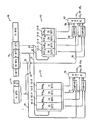
- the figure is a schematic block diagram of an embodiment of a data processing system including a translation lookaside buffer and a lock bit storage array according to the principles of the present invention.
- the lock bits are placed in a separate array LBA (Lock Bit Array) which has approximately 1/10 as many entries as the TLB.
- LBA Lock Bit Array
- a schematic illustration of a data buffer system is shown including a translation lookaside buffer storage means 10 and a lock bit array storage means 12.
- the translation lookaside buffer 10 in this specific illustration, contains two virtual address locations 10-2 and 10-4 (VA and VA b ) having 128 rows of 25 bits and-contains two corresponding real address (RA) locations 10-6 and 10-8 with 128 rows of 15 bits.
- the lock bit array storage means 12 is similarly organized with two storage areas 12-2 and 12-4 for virtual addresses (VA' a and VA' b ) each 29 bits wide and two storage areas 12-6, 12-8 for lock bits, LB a and LB b each 32 bits wide.
- Lock bit array storage 12 has eight rows.
- a segment register 14 is provided containing the aforesaid "S" bit (0 or 1) and 15 segment identification bits.
- the 15 segment identification bits from register 14 on line 30 are combined with the 10 higher order N v bits from register 16 on line 32 as well as the aforesaid 4, lower order N v bits on line 34. These combined 29 bits on line 36 are applied to compare circuit 38 and compare circuit 40. If there is a match in compare circuit 38 with the 29 VA' a bits from location 12-2, a FlA signal is generated and applied to gate circuit 42 to gate out 32 lock bits LB a from location 12-4. Likewise, the 29 bits on line 36 are compared with the 29 VA' b bits in compare circuit . 40, and if a match occurs, an F1 B signal is produced which is applied to gate 42 to gate through the 32 LB B lock bits from location 12-8.
Landscapes
- Engineering & Computer Science (AREA)
- Theoretical Computer Science (AREA)
- Physics & Mathematics (AREA)
- General Engineering & Computer Science (AREA)
- General Physics & Mathematics (AREA)
- Computer Security & Cryptography (AREA)
- Memory System Of A Hierarchy Structure (AREA)
Applications Claiming Priority (2)
| Application Number | Priority Date | Filing Date | Title |
|---|---|---|---|
| US560479 | 1983-12-12 | ||
| US06/560,479 US4589092A (en) | 1983-12-12 | 1983-12-12 | Data buffer having separate lock bit storage array |
Publications (3)
| Publication Number | Publication Date |
|---|---|
| EP0144763A2 true EP0144763A2 (de) | 1985-06-19 |
| EP0144763A3 EP0144763A3 (en) | 1988-03-30 |
| EP0144763B1 EP0144763B1 (de) | 1990-06-13 |
Family
ID=24237988
Family Applications (1)
| Application Number | Title | Priority Date | Filing Date |
|---|---|---|---|
| EP84113323A Expired EP0144763B1 (de) | 1983-12-12 | 1984-11-06 | Adressumsetzungsgerät für eine Datenverarbeitungsanordnung mit virtuellem Speicher |
Country Status (4)
| Country | Link |
|---|---|
| US (1) | US4589092A (de) |
| EP (1) | EP0144763B1 (de) |
| JP (1) | JPS60128545A (de) |
| DE (1) | DE3482511D1 (de) |
Cited By (1)
| Publication number | Priority date | Publication date | Assignee | Title |
|---|---|---|---|---|
| US6973557B2 (en) * | 2003-02-04 | 2005-12-06 | Sun Microsystems, Inc. | Apparatus and method for dual access to a banked and pipelined data cache memory unit |
Families Citing this family (32)
| Publication number | Priority date | Publication date | Assignee | Title |
|---|---|---|---|---|
| JPS61206057A (ja) * | 1985-03-11 | 1986-09-12 | Hitachi Ltd | アドレス変換装置 |
| US5029072A (en) * | 1985-12-23 | 1991-07-02 | Motorola, Inc. | Lock warning mechanism for a cache |
| US5291581A (en) * | 1987-07-01 | 1994-03-01 | Digital Equipment Corporation | Apparatus and method for synchronization of access to main memory signal groups in a multiprocessor data processing system |
| US4980816A (en) * | 1987-12-18 | 1990-12-25 | Nec Corporation | Translation look-aside buffer control system with multiple prioritized buffers |
| JP2504137B2 (ja) * | 1988-09-27 | 1996-06-05 | 日本電気株式会社 | メモリ書き込みプロテクト回路 |
| US4926481A (en) * | 1988-12-05 | 1990-05-15 | The United States Of America As Represented By The Administrator Of The National Aeronautics And Space Administration | Computer access security code system |
| FR2645987B1 (fr) * | 1989-04-13 | 1991-06-07 | Bull Sa | Dispositif d'acceleration des acces memoire dans un systeme informatique |
| US5265227A (en) * | 1989-11-14 | 1993-11-23 | Intel Corporation | Parallel protection checking in an address translation look-aside buffer |
| US5485594A (en) * | 1992-07-17 | 1996-01-16 | International Business Machines Corporation | Apparatus and method using an atomic fetch and add for establishing temporary ownership of a common system resource in a multiprocessor data processing system |
| US5974508A (en) * | 1992-07-31 | 1999-10-26 | Fujitsu Limited | Cache memory system and method for automatically locking cache entries to prevent selected memory items from being replaced |
| US5450563A (en) * | 1992-10-30 | 1995-09-12 | International Business Machines Corporation | Storage protection keys in two level cache system |
| US5809525A (en) * | 1993-09-17 | 1998-09-15 | International Business Machines Corporation | Multi-level computer cache system providing plural cache controllers associated with memory address ranges and having cache directories |
| US5872980A (en) * | 1996-01-25 | 1999-02-16 | International Business Machines Corporation | Semaphore access control buffer and method for accelerated semaphore operations |
| US5954818A (en) * | 1997-02-03 | 1999-09-21 | Intel Corporation | Method of programming, erasing, and reading block lock-bits and a master lock-bit in a flash memory device |
| US6073243A (en) * | 1997-02-03 | 2000-06-06 | Intel Corporation | Block locking and passcode scheme for flash memory |
| US6035401A (en) * | 1997-02-03 | 2000-03-07 | Intel Corporation | Block locking apparatus for flash memory |
| US6412056B1 (en) | 1997-10-01 | 2002-06-25 | Compac Information Technologies Group, Lp | Extended translation lookaside buffer with fine-grain state bits |
| US6268850B1 (en) | 1997-12-22 | 2001-07-31 | Sun Microsystems, Inc. | User interface for the specification of lock groups |
| US6240413B1 (en) * | 1997-12-22 | 2001-05-29 | Sun Microsystems, Inc. | Fine-grained consistency mechanism for optimistic concurrency control using lock groups |
| US6385618B1 (en) | 1997-12-22 | 2002-05-07 | Sun Microsystems, Inc. | Integrating both modifications to an object model and modifications to a database into source code by an object-relational mapping tool |
| US6175837B1 (en) | 1998-06-29 | 2001-01-16 | Sun Microsystems, Inc. | Object-relational mapping toll that processes views |
| US6374256B1 (en) | 1997-12-22 | 2002-04-16 | Sun Microsystems, Inc. | Method and apparatus for creating indexes in a relational database corresponding to classes in an object-oriented application |
| US6360223B1 (en) | 1997-12-22 | 2002-03-19 | Sun Microsystems, Inc. | Rule-based approach to object-relational mapping strategies |
| US6363336B1 (en) * | 1999-10-13 | 2002-03-26 | Transmeta Corporation | Fine grain translation discrimination |
| US6529983B1 (en) * | 1999-11-03 | 2003-03-04 | Cisco Technology, Inc. | Group and virtual locking mechanism for inter processor synchronization |
| US6591275B1 (en) | 2000-06-02 | 2003-07-08 | Sun Microsystems, Inc. | Object-relational mapping for tables without primary keys |
| EP1182569B8 (de) * | 2000-08-21 | 2011-07-06 | Texas Instruments Incorporated | TLB-Ver- und Entriegelungsoperation |
| US6681311B2 (en) * | 2001-07-18 | 2004-01-20 | Ip-First, Llc | Translation lookaside buffer that caches memory type information |
| KR100520301B1 (ko) * | 2001-10-13 | 2005-10-13 | 한국전자통신연구원 | 객체관계형 데이터베이스 관리 시스템 및 그것의 클래스인스턴스 삭제 방법 |
| US7398554B1 (en) * | 2002-04-02 | 2008-07-08 | Winbond Electronics Corporation | Secure lock mechanism based on a lock word |
| US7185170B2 (en) * | 2004-08-27 | 2007-02-27 | Freescale Semiconductor, Inc. | Data processing system having translation lookaside buffer valid bits with lock and method therefor |
| US9558121B2 (en) * | 2012-12-28 | 2017-01-31 | Intel Corporation | Two-level cache locking mechanism |
Family Cites Families (9)
| Publication number | Priority date | Publication date | Assignee | Title |
|---|---|---|---|---|
| US4037214A (en) * | 1976-04-30 | 1977-07-19 | International Business Machines Corporation | Key register controlled accessing system |
| JPS52149444A (en) * | 1976-06-08 | 1977-12-12 | Fujitsu Ltd | Multiplex virtual space processing data processing system |
| US4136385A (en) * | 1977-03-24 | 1979-01-23 | International Business Machines Corporation | Synonym control means for multiple virtual storage systems |
| US4096573A (en) * | 1977-04-25 | 1978-06-20 | International Business Machines Corporation | DLAT Synonym control means for common portions of all address spaces |
| US4170039A (en) * | 1978-07-17 | 1979-10-02 | International Business Machines Corporation | Virtual address translation speed up technique |
| JPS5576447A (en) * | 1978-12-01 | 1980-06-09 | Fujitsu Ltd | Address control system for software simulation |
| US4332010A (en) * | 1980-03-17 | 1982-05-25 | International Business Machines Corporation | Cache synonym detection and handling mechanism |
| US4400770A (en) * | 1980-11-10 | 1983-08-23 | International Business Machines Corporation | Cache synonym detection and handling means |
| US4513367A (en) * | 1981-03-23 | 1985-04-23 | International Business Machines Corporation | Cache locking controls in a multiprocessor |
-
1983
- 1983-12-12 US US06/560,479 patent/US4589092A/en not_active Expired - Fee Related
-
1984
- 1984-11-06 EP EP84113323A patent/EP0144763B1/de not_active Expired
- 1984-11-06 DE DE8484113323T patent/DE3482511D1/de not_active Expired - Lifetime
- 1984-11-14 JP JP59238702A patent/JPS60128545A/ja active Granted
Cited By (1)
| Publication number | Priority date | Publication date | Assignee | Title |
|---|---|---|---|---|
| US6973557B2 (en) * | 2003-02-04 | 2005-12-06 | Sun Microsystems, Inc. | Apparatus and method for dual access to a banked and pipelined data cache memory unit |
Also Published As
| Publication number | Publication date |
|---|---|
| US4589092A (en) | 1986-05-13 |
| DE3482511D1 (de) | 1990-07-19 |
| EP0144763B1 (de) | 1990-06-13 |
| JPS60128545A (ja) | 1985-07-09 |
| JPH0315211B2 (de) | 1991-02-28 |
| EP0144763A3 (en) | 1988-03-30 |
Similar Documents
| Publication | Publication Date | Title |
|---|---|---|
| EP0144763B1 (de) | Adressumsetzungsgerät für eine Datenverarbeitungsanordnung mit virtuellem Speicher | |
| US4654777A (en) | Segmented one and two level paging address translation system | |
| US5628023A (en) | Virtual storage computer system having methods and apparatus for providing token-controlled access to protected pages of memory via a token-accessible view | |
| US4136385A (en) | Synonym control means for multiple virtual storage systems | |
| US6014732A (en) | Cache memory with reduced access time | |
| US5412787A (en) | Two-level TLB having the second level TLB implemented in cache tag RAMs | |
| KR900005897B1 (ko) | 마이크로프로세서 시스템과 그 메모리 운용장치 | |
| US4905141A (en) | Partitioned cache memory with partition look-aside table (PLAT) for early partition assignment identification | |
| KR920005280B1 (ko) | 고속 캐쉬 시스템 | |
| US5375214A (en) | Single translation mechanism for virtual storage dynamic address translation with non-uniform page sizes | |
| US5230045A (en) | Multiple address space system including address translator for receiving virtual addresses from bus and providing real addresses on the bus | |
| US5265227A (en) | Parallel protection checking in an address translation look-aside buffer | |
| US4096573A (en) | DLAT Synonym control means for common portions of all address spaces | |
| US6493812B1 (en) | Apparatus and method for virtual address aliasing and multiple page size support in a computer system having a prevalidated cache | |
| JP3666689B2 (ja) | 仮想アドレス変換方法 | |
| CA2057494A1 (en) | Translation lookaside buffer | |
| US5530823A (en) | Hit enhancement circuit for page-table-look-aside-buffer | |
| US5305444A (en) | Apparatus for increasing the number of hits in a translation lookaside buffer including instruction address lookaside register | |
| US6571316B1 (en) | Cache memory array for multiple address spaces | |
| US5050126A (en) | Buffer memory control apparatus | |
| EP0708404A2 (de) | Verschachtelte Datencache-Speichermatrix mit mehreren inhaltadressierbaren Feldern per Cache-Speicherzeile | |
| US4943914A (en) | Storage control system in which real address portion of TLB is on same chip as BAA | |
| EP0284751B1 (de) | Cache-Speicher | |
| US5890221A (en) | Method and system for offset miss sequence handling in a data cache array having multiple content addressable field per cache line utilizing an MRU bit | |
| US5652860A (en) | Memory control device |
Legal Events
| Date | Code | Title | Description |
|---|---|---|---|
| PUAI | Public reference made under article 153(3) epc to a published international application that has entered the european phase |
Free format text: ORIGINAL CODE: 0009012 |
|
| 17P | Request for examination filed |
Effective date: 19841214 |
|
| AK | Designated contracting states |
Designated state(s): DE FR GB |
|
| PUAL | Search report despatched |
Free format text: ORIGINAL CODE: 0009013 |
|
| AK | Designated contracting states |
Kind code of ref document: A3 Designated state(s): DE FR GB |
|
| 17Q | First examination report despatched |
Effective date: 19890908 |
|
| GRAA | (expected) grant |
Free format text: ORIGINAL CODE: 0009210 |
|
| AK | Designated contracting states |
Kind code of ref document: B1 Designated state(s): DE FR GB |
|
| REF | Corresponds to: |
Ref document number: 3482511 Country of ref document: DE Date of ref document: 19900719 |
|
| ET | Fr: translation filed | ||
| PLBE | No opposition filed within time limit |
Free format text: ORIGINAL CODE: 0009261 |
|
| STAA | Information on the status of an ep patent application or granted ep patent |
Free format text: STATUS: NO OPPOSITION FILED WITHIN TIME LIMIT |
|
| 26N | No opposition filed | ||
| PGFP | Annual fee paid to national office [announced via postgrant information from national office to epo] |
Ref country code: FR Payment date: 19941103 Year of fee payment: 11 |
|
| PGFP | Annual fee paid to national office [announced via postgrant information from national office to epo] |
Ref country code: DE Payment date: 19941201 Year of fee payment: 11 |
|
| PGFP | Annual fee paid to national office [announced via postgrant information from national office to epo] |
Ref country code: GB Payment date: 19951024 Year of fee payment: 12 |
|
| PG25 | Lapsed in a contracting state [announced via postgrant information from national office to epo] |
Ref country code: FR Effective date: 19960731 |
|
| PG25 | Lapsed in a contracting state [announced via postgrant information from national office to epo] |
Ref country code: DE Effective date: 19960801 |
|
| REG | Reference to a national code |
Ref country code: FR Ref legal event code: ST |
|
| PG25 | Lapsed in a contracting state [announced via postgrant information from national office to epo] |
Ref country code: GB Effective date: 19961106 |
|
| GBPC | Gb: european patent ceased through non-payment of renewal fee |
Effective date: 19961106 |