EP0145036B1 - Dispositif semi-conducteur ayant une structure d'interconnexion - Google Patents
Dispositif semi-conducteur ayant une structure d'interconnexion Download PDFInfo
- Publication number
- EP0145036B1 EP0145036B1 EP84201319A EP84201319A EP0145036B1 EP 0145036 B1 EP0145036 B1 EP 0145036B1 EP 84201319 A EP84201319 A EP 84201319A EP 84201319 A EP84201319 A EP 84201319A EP 0145036 B1 EP0145036 B1 EP 0145036B1
- Authority
- EP
- European Patent Office
- Prior art keywords
- conductor tracks
- layer
- semiconductor device
- semiconductor
- silicon
- Prior art date
- Legal status (The legal status is an assumption and is not a legal conclusion. Google has not performed a legal analysis and makes no representation as to the accuracy of the status listed.)
- Expired
Links
Images


Classifications
-
- H—ELECTRICITY
- H10—SEMICONDUCTOR DEVICES; ELECTRIC SOLID-STATE DEVICES NOT OTHERWISE PROVIDED FOR
- H10W—GENERIC PACKAGES, INTERCONNECTIONS, CONNECTORS OR OTHER CONSTRUCTIONAL DETAILS OF DEVICES COVERED BY CLASS H10
- H10W70/00—Package substrates; Interposers; Redistribution layers [RDL]
- H10W70/20—Conductive package substrates serving as an interconnection, e.g. metal plates
- H10W70/24—Conductive package substrates serving as an interconnection, e.g. metal plates characterised by materials
- H10W70/26—Semiconductor materials
-
- H—ELECTRICITY
- H10—SEMICONDUCTOR DEVICES; ELECTRIC SOLID-STATE DEVICES NOT OTHERWISE PROVIDED FOR
- H10W—GENERIC PACKAGES, INTERCONNECTIONS, CONNECTORS OR OTHER CONSTRUCTIONAL DETAILS OF DEVICES COVERED BY CLASS H10
- H10W20/00—Interconnections in chips, wafers or substrates
- H10W20/40—Interconnections external to wafers or substrates, e.g. back-end-of-line [BEOL] metallisations or vias connecting to gate electrodes
-
- Y—GENERAL TAGGING OF NEW TECHNOLOGICAL DEVELOPMENTS; GENERAL TAGGING OF CROSS-SECTIONAL TECHNOLOGIES SPANNING OVER SEVERAL SECTIONS OF THE IPC; TECHNICAL SUBJECTS COVERED BY FORMER USPC CROSS-REFERENCE ART COLLECTIONS [XRACs] AND DIGESTS
- Y10—TECHNICAL SUBJECTS COVERED BY FORMER USPC
- Y10S—TECHNICAL SUBJECTS COVERED BY FORMER USPC CROSS-REFERENCE ART COLLECTIONS [XRACs] AND DIGESTS
- Y10S257/00—Active solid-state devices, e.g. transistors, solid-state diodes
- Y10S257/914—Polysilicon containing oxygen, nitrogen, or carbon, e.g. sipos
Definitions
- the invention relates to a semiconductor device comprising a semiconductor body of silicon having at a first main surface a conductor structure consisting of conductor tracks which are spaced apart, which comprise silicon of opposite conductivity types and which are connected to each other in an electrically conducting manner.
- Such an undesired pn junction may be shortcircuited by a conductive connection in the form of a strip of conducting material provided between the oppositely doped tracks.
- the conductive material may be provided afterwards by providing a metal strip on the pn junction or by silicidation of the silicon on either side of the pn junction (see for example the Dutch Patent Application Nr. 8105920 (PHN 10.227) (EP-A-0083816) of the Applicant laid open to public inspection on July 18th 1983 and Japanese Kokai Nr. 56-04671).
- a semiconductor device of the kind mentioned in the opening paragraph is known from the Dutch Patent Application Nr. 8105559 (PHN 10.211) (US-A-4449287) of the Applicant laid open to public inspection on July 1st 1983.
- the oppositely doped tracks of polycrystalline silicon to be connected to each other are spaced apart by a certain distance and are separated from each other by a groove generally filled with oxide.
- connection is rather provided afterwards, preferably together with other conductor tracks, contact metallizations or, for example, a metal which forms with the subjacent silicon a Schottky diode.
- a device is characterized in that at least at the area of the conductive connection the conductor tracks are located on the semiconductor surface and are connected to each other by means of a layer of metal silicide which is located on the semiconductor surface between the conductor tracks and which contacts parts of the conductor tracks.
- the invention is based on the recognition of the fact that in given applications, notably in the manufacture of very small memory cells, such a connection can be situated directly on the semiconductor surface without the function of the subjacent semiconductor region being influenced by a partial doping of an opposite conductivity type.
- connection may be manufactured, if desired, entirely in a self-aligning manner.
- the conductor tracks are coated with an oxide layer having a contact window at the area of the conductive connection, the metal silicide being situated only within the contact window.
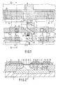
- the memory cell of Figures 1 to 4 comprises a semiconductor body 1 having at a major surface 2 two cross-coupled npn transistors 25, 25', whose emitters 18, 18' are connected to each other and are further connected to a first word line 27, whilst the collector of the transistor 25 is connected to the base of the transistor 25' and the collector of the transistor 25' is connected to the base of the transistor 25.
- the load is constituted by pnp transistors 20, 20', whose emitters 15, 15' are connected to a second word line 28, whilst the bases (16, 16') and the collectors (17, 17') at the same time constitute the collectors and bases of the cross-coupled transistors 25, 25'.
- the last- mentioned transistors moreover each have a second emitter 19,19', which is connected to a bit line 29, via which information can be written or read.
- the active regions in which the transistors 20, 20', 25, 25' are formed are insulated from each other by means of a layer of sunken oxide 3, whose boundary is indicated in the planeview of Figure 1 by dot-and-dash lines 11, 12, 13, 14.
- the semiconductor body comprises a p-type substrate 4 on which an epitaxial layer 5 of the n-type is grown.
- the semiconductor device is further provided with buried layers 6, which pass underneath the sunken oxide at the desired areas. At the areas at which the buried layers 6 extend outside the regions 11, 12, 13, 14 under the sunken oxide 3 this is indicated in Figure 1 by broken lines.
- a pattern of polycrystalline silicon tracks which are either p-type conducting (reference numeral 7) or n-type conducting (reference numeral 8), and a metallization pattern 9 extend on the surface 2.
- polycrystalline silicon regions of opposite conductivity type are mutually separated by an electrically insulating layer 10 of, for example, silicon oxide. This layer 10 also insulates the conductor tracks 9 from the polycrystalline silicon and acts at other areas as a protective layer.
- a lateral pnp transistor 20 is formed in each of the openings 11, 13 in the sunken oxide, where (see Figure 2) the p-type region 15 acts as the emitter, the n-type conducting region 16 forming part of the epitaxial layer 5 acts as the base and the p-type region 17 acts as the collector.
- the n-type region 16 constitutes together with the buried layer 6 and a part of the epitaxial layer 5 the collector of an npn transistor 25, whose base is constituted by a p-type region 17 and which has two emitter regions 18, 19.
- the p-type region 17 is further provided with p-type contact zones 26.
- the semiconductor device shown in Figures 1 to 4 comprises at the area of the opening 12 in the sunken oxide a shortcircuit 21 between the said p-type polycrystalline silicon track 7 and an n-type polycrystalline silicon track 8 contacting an n +- region 22 within the opening 12.
- the said p-type track 7 contacts a p-type region 23 which does not adversely affect the operation of the circuit.
- the shortcircuit 21 itself is constituted, for example, by a layer of platinum silicide having a thickness of about 50 nm.
- the platinum silicide 21 contacting both the two polycrystalline tracks 7, 8 and the surface of the epitaxial layer between said tracks and the n-type zones 22, 5, 6 a low-ohmic connection is now formed between the base 17 of the transistor 25 and the collector 16' of the transistor 25' cross-coupled with the transistor 25.
- the p-type polycrystalline layer 7 contacting the base of the transistor 25' is connected in an electrically conducting manner to an n-type polycrystalline semiconductor region 8 and an intermediate exposed semiconductor region where the area at which the buried region 6 extends, which buried region forms part of the collector of the transistor 25.
- Such shortcircuits 21 of tracks of polycrystalline silicon spaced apart by a small distance are possible according to the invention because the conductivity type of the subjacent semiconductor region is mainly determined by the impurities which determine the conductivity type of one polycrystalline silicon track, whereas impurities originating from the other polycrystalline silicon track do not influence the actual operation of the shortcircuited contact in the electric circuit, in this case a memory circuit.
- the word and bit lines are present further in the form of aluminium tracks 9 which, where required, contact the subjacent polycrystalline silicon via contact holes 24.
- the starting material is a semiconductor body 1 which is provided at its surface 2 with sunken oxide regions 3, which define active regions, in which the transistors 20, 25 are formed.
- the semiconductor body 1 is obtained, for example, by first defining the buried layers 6 in a p-type substrate 4 and by then growing the epitaxial layer 5 by means of generally known techniques, after which the sunken oxide regions 3 are defined at the desired areas by means of local oxidation.
- a first silicon layer 31, an overlying oxidation-preventing layer 32, in this example of silicon nitride, and an overlying oxidizable layer 33, in this example a second silicon layer, are successively deposited on the surface 2 of the semiconductor body 1 by the use of deposition methods generally known in semiconductor technology. Moreover, a further oxidation-preventing layer 34 having a larger thickness than the layer 32 and consisting in this example also of silicon nitride is further formed on the second silicon layer 33. It should further be noted that between the silicon nitride layers 32 and 34 and the subjacent silicon layers 31 and 33 a very thin oxide layer (not shown) is sometimes provided.
- the layers 31 and 33 in this example are substantially undoped polycrystalline silicon layers having a thickness of 0.5 pm and 0.35 pm, respectively.
- the nitride layers 32 and 34 have a thickness of 75 nm and 150 nm, respectively.
- an edge portion 35 of the remaining part of the oxidizable silicon layer 33 is oxidized throughout its thickness.
- the silicon nitride layers 32 and 34 protect the subjacent silicon layers 31 and 33 from oxidation.
- the oxidized edge portion 35 in this example has a width of about 0.9 pm (see Figure 6).
- the uncovered part of the first oxidation-preventing layer 32 (inclusive of a possibly subjacent very thin oxide layer) is then removed.
- the nitride layer 34 is partly maintained because it is thicker than the layer 32.
- the oxidized edge portion 35 is removed by means of etching, after which the exposed part of the first silicon layer 31 is oxidized by heating in an oxygen- containing atmosphere over part of its thickness, just like the edge of the layer 33.
- a thermal oxide layer 36 having a thickness of, for example, 0.15 um, is formed.
- a part (approximately 0.8 ⁇ m) of the nitride layer 32 remains uncovered (see Figure 7).
- the second oxidation-preventing layer 34 and the part of the oxidation-preventing layer 32 exposed by the removal of the edge portion 35 are then successively removed by etching.
- the polycrystalline silicon layer 33 is etched away, in which process also a groove 38 is etched into the layer 31 at the area of the exposed polycrystalline silicon of this layer.
- an oxide layer 40 is formed in the groove, the part of the polycrystalline silicon layer 31 located under the remaining nitride layer 32 being protected from this thermal oxidation (see Figure 9).
- This remaining part of the layer 32 is then selectively etched away at the area of the collector contact regions to be formed, after which a donor implantation or diffusion, for example, with phosphorus, is carried out.
- the uncovered parts 8 of the silicon layer 31 then obtain a high n-type doping.
- a phosphorus implantation is carried out, this may also take place when the layer 32 is still present.
- the arsenic diffuses from the layer 1 into the subjacent semiconductor body and there forms the n-type collector contact zone 22 (see Figure 10).
- the parts of the silicon layer 31 not located under the layers 33 are doped with an acceptor, for example with boron. This may take place by means of ion implantation (which may be carried out through the nitride layer 32) both at the stage shown in Figure 5 and at the stage shown in Figure 6 and by means of diffusion immediately before the stage shown in Figure 6.
- the highly doped p-type conducting parts 7 of the layer 31 thus obtained form good ohmic contacts on the p-type zones 23, 15 and 17 and at the same time act as a diffusion source for the zones 23, 15 and the base contact zones 26 for the p-type base zones 17.
- the second silicon layer 33 and the oxidized edge portion 35 thereof act as a mask during the said doping.
- the exposed parts of the layer 31 are covered with an oxide layer 10 by means of thermal oxidation.
- the remaining part of the nitride layer 32 is removed, after which at these areas the intrinsic bases 17 and the emitter regions 18, 19 are formed by means of a boron implantation and a subsequent arsenic implantation, respectively.
- a contact window 39 is now formed in the oxide layer 10 at the area of the groove 38.
- the conductive connection 21 is firmed in this contact window by silicidation of the surface 2 of the semiconductor body exposed in the groove 38 and of the polycrystalline silicon tracks 7,31 and 8,31.
- the semiconductor body is covered with a metal layer, in this case of platinum, which is then converted by heating into platinum silicide at those areas at which the platinum is in contact with silicon.
- the platinum left on the oxide layer 10 is then removed by etching.
- the platinum silicide is formed in a self-aligning manner inside the contact windows 39 (see Figure 11).
- contacts of platinum silicide may be applied, which form, for example, with the subjacent silicon, a Schottky diode.
- the platinum silicide is simultaneously formed in other contact windows 24 in the oxide layer 10, after which the surface is covered with an aluminium layer from which the metallization pattern 9 is formed photolithographically.
- the device shown in Figures 1 to 3 is obtained.
- the conductor tracks 7, 8, 9 may be provided, if required, with external connection conductors.
- the invention is of course not limited to the embodiment described above.
- other oxidizable layer materials such as aluminium, hafnium or zirconium, may be chosen.
- a shortcircuit may alternatively be manufactured by other methods, in which two semiconductor tracks of opposite conductivity types are formed at a short relative distance (of the order of 1 11m or less), as is the case, for example, with the method shown in Japanese Kokai Nr. 54-154966 or in the article "1.25 pm Deep-Groove-Isolated Self-Aligned Bipolar Circuits" by D. D. Tang et a/, published in I.E.E.E. Journal of Solid State Circuits, Vol. SC-17, Nr.
- the thin oxide which in this case separates two polycrystalline silicon layers overlapping each other in part, is then etched away down to the semiconductor body, after which a metal silicide is formed again on the semiconductor body and on parts of the polycrystalline silicon layers.
- the starting material is a single polycrystalline silicon layer, as shown, for example, in Proceedings of the I.E.E.E. International Solid State Circuits Conference, February 1981, pages 216-217 or in the article "A 3-ns 1-kBIT RAM Using Super-Self-Aligned Process Technology", by T. Sakai et al, published in I.E.E.E. Journal of Solid State Circuits, Vol. SC-16, Nr. 5, October 1981, pages 424-429.
Landscapes
- Semiconductor Memories (AREA)
- Bipolar Transistors (AREA)
- Internal Circuitry In Semiconductor Integrated Circuit Devices (AREA)
- Electrodes Of Semiconductors (AREA)
Claims (8)
Applications Claiming Priority (2)
| Application Number | Priority Date | Filing Date | Title |
|---|---|---|---|
| NL8303179 | 1983-09-15 | ||
| NL8303179A NL8303179A (nl) | 1983-09-15 | 1983-09-15 | Halfgeleiderinrichting. |
Publications (2)
| Publication Number | Publication Date |
|---|---|
| EP0145036A1 EP0145036A1 (fr) | 1985-06-19 |
| EP0145036B1 true EP0145036B1 (fr) | 1988-01-07 |
Family
ID=19842401
Family Applications (1)
| Application Number | Title | Priority Date | Filing Date |
|---|---|---|---|
| EP84201319A Expired EP0145036B1 (fr) | 1983-09-15 | 1984-09-12 | Dispositif semi-conducteur ayant une structure d'interconnexion |
Country Status (6)
| Country | Link |
|---|---|
| US (1) | US4680619A (fr) |
| EP (1) | EP0145036B1 (fr) |
| JP (1) | JPS60143661A (fr) |
| CA (1) | CA1224279A (fr) |
| DE (1) | DE3468589D1 (fr) |
| NL (1) | NL8303179A (fr) |
Family Cites Families (14)
| Publication number | Priority date | Publication date | Assignee | Title |
|---|---|---|---|---|
| NL7612883A (nl) * | 1976-11-19 | 1978-05-23 | Philips Nv | Halfgeleiderinrichting, en werkwijze ter ver- vaardiging daarvan. |
| US4333099A (en) * | 1978-02-27 | 1982-06-01 | Rca Corporation | Use of silicide to bridge unwanted polycrystalline silicon P-N junction |
| JPS55134962A (en) * | 1979-04-09 | 1980-10-21 | Toshiba Corp | Semiconductor device |
| CA1142261A (fr) * | 1979-06-29 | 1983-03-01 | Siegfried K. Wiedmann | Methode d'interconnexion de regions semiconductrices de types opposes |
| JPS5694671A (en) * | 1979-12-27 | 1981-07-31 | Fujitsu Ltd | Manufacture of mis field-effect semiconductor device |
| US4336550A (en) * | 1980-03-20 | 1982-06-22 | Rca Corporation | CMOS Device with silicided sources and drains and method |
| US4403394A (en) * | 1980-12-17 | 1983-09-13 | International Business Machines Corporation | Formation of bit lines for ram device |
| US4476482A (en) * | 1981-05-29 | 1984-10-09 | Texas Instruments Incorporated | Silicide contacts for CMOS devices |
| US4617071A (en) * | 1981-10-27 | 1986-10-14 | Fairchild Semiconductor Corporation | Method of fabricating electrically connected regions of opposite conductivity type in a semiconductor structure |
| US4622575A (en) * | 1981-10-27 | 1986-11-11 | Fairchild Semiconductor Corporation | Integrated circuit bipolar memory cell |
| US4488350A (en) * | 1981-10-27 | 1984-12-18 | Fairchild Camera & Instrument Corp. | Method of making an integrated circuit bipolar memory cell |
| NL8105559A (nl) * | 1981-12-10 | 1983-07-01 | Philips Nv | Werkwijze voor het aanbrengen van een smalle groef in een substraatgebied, in het bijzonder een halfgeleidersubstraatgebied. |
| NL8105920A (nl) * | 1981-12-31 | 1983-07-18 | Philips Nv | Halfgeleiderinrichting en werkwijze voor het vervaardigen van een dergelijke halfgeleiderinrichting. |
| US4543595A (en) * | 1982-05-20 | 1985-09-24 | Fairchild Camera And Instrument Corporation | Bipolar memory cell |
-
1983
- 1983-09-15 NL NL8303179A patent/NL8303179A/nl not_active Application Discontinuation
-
1984
- 1984-08-31 US US06/645,897 patent/US4680619A/en not_active Expired - Fee Related
- 1984-09-12 JP JP59189813A patent/JPS60143661A/ja active Pending
- 1984-09-12 DE DE8484201319T patent/DE3468589D1/de not_active Expired
- 1984-09-12 EP EP84201319A patent/EP0145036B1/fr not_active Expired
- 1984-09-13 CA CA000463087A patent/CA1224279A/fr not_active Expired
Also Published As
| Publication number | Publication date |
|---|---|
| DE3468589D1 (en) | 1988-02-11 |
| CA1224279A (fr) | 1987-07-14 |
| JPS60143661A (ja) | 1985-07-29 |
| NL8303179A (nl) | 1985-04-01 |
| US4680619A (en) | 1987-07-14 |
| EP0145036A1 (fr) | 1985-06-19 |
Similar Documents
| Publication | Publication Date | Title |
|---|---|---|
| US4543595A (en) | Bipolar memory cell | |
| EP0170250B1 (fr) | Transistor bipolaire et son procédé de fabrication | |
| EP0021403B1 (fr) | Circuits semiconducteurs autoalignés | |
| US4161745A (en) | Semiconductor device having non-metallic connection zones | |
| EP0201867B1 (fr) | Procédé de fabrication d'un transistor bipolaire | |
| EP0064466A2 (fr) | Structure logique utilisant des diodes Schottky en silicium polycristallin | |
| EP0080730B1 (fr) | Dispositif semi-conducteur comprenant des couches conductrices et procédé pour le fabriquer | |
| US4425379A (en) | Polycrystalline silicon Schottky diode array | |
| EP0084500B1 (fr) | Cellules mémoire pour RAM de haute densité réalisées par implantation ionique | |
| US4539742A (en) | Semiconductor device and method for manufacturing the same | |
| EP0078501A2 (fr) | Dispositif semi-conducteur de type transistor et son procédé de fabrication | |
| EP0030147B1 (fr) | Procédé de fabrication d'un circuit intégré à semi-conducteur | |
| EP0051534B1 (fr) | Procédé de fabrication auto-alignée de structures de circuits intégrés employant différents taux de croissance de l'oxyde | |
| EP0078220B1 (fr) | Interférences de silicium polycristallin pour transistors bipolaires en circuit flip-flop | |
| US4691436A (en) | Method for fabricating a bipolar semiconductor device by undercutting and local oxidation | |
| JPH06105765B2 (ja) | 半導体romアレイを作成するプロセス | |
| JPH0241170B2 (fr) | ||
| US4628339A (en) | Polycrystalline silicon Schottky diode array | |
| US4883772A (en) | Process for making a self-aligned silicide shunt | |
| JPS62179764A (ja) | 壁スペ−サを有するバイポ−ラ半導体装置の製造方法 | |
| US4799099A (en) | Bipolar transistor in isolation well with angled corners | |
| EP0145036B1 (fr) | Dispositif semi-conducteur ayant une structure d'interconnexion | |
| US4512076A (en) | Semiconductor device fabrication process | |
| US4695856A (en) | Semiconductor device | |
| CA1205577A (fr) | Dispositif semiconducteur |
Legal Events
| Date | Code | Title | Description |
|---|---|---|---|
| PUAI | Public reference made under article 153(3) epc to a published international application that has entered the european phase |
Free format text: ORIGINAL CODE: 0009012 |
|
| AK | Designated contracting states |
Designated state(s): DE FR GB IT NL |
|
| 17P | Request for examination filed |
Effective date: 19851218 |
|
| 17Q | First examination report despatched |
Effective date: 19870324 |
|
| GRAA | (expected) grant |
Free format text: ORIGINAL CODE: 0009210 |
|
| AK | Designated contracting states |
Kind code of ref document: B1 Designated state(s): DE FR GB IT NL |
|
| REF | Corresponds to: |
Ref document number: 3468589 Country of ref document: DE Date of ref document: 19880211 |
|
| ITF | It: translation for a ep patent filed | ||
| ET | Fr: translation filed | ||
| PLBE | No opposition filed within time limit |
Free format text: ORIGINAL CODE: 0009261 |
|
| STAA | Information on the status of an ep patent application or granted ep patent |
Free format text: STATUS: NO OPPOSITION FILED WITHIN TIME LIMIT |
|
| 26N | No opposition filed | ||
| PGFP | Annual fee paid to national office [announced via postgrant information from national office to epo] |
Ref country code: NL Payment date: 19890930 Year of fee payment: 6 |
|
| PGFP | Annual fee paid to national office [announced via postgrant information from national office to epo] |
Ref country code: GB Payment date: 19900831 Year of fee payment: 7 |
|
| PGFP | Annual fee paid to national office [announced via postgrant information from national office to epo] |
Ref country code: FR Payment date: 19900920 Year of fee payment: 7 |
|
| ITTA | It: last paid annual fee | ||
| PGFP | Annual fee paid to national office [announced via postgrant information from national office to epo] |
Ref country code: DE Payment date: 19901123 Year of fee payment: 7 |
|
| PG25 | Lapsed in a contracting state [announced via postgrant information from national office to epo] |
Ref country code: NL Effective date: 19910401 |
|
| NLV4 | Nl: lapsed or anulled due to non-payment of the annual fee | ||
| PG25 | Lapsed in a contracting state [announced via postgrant information from national office to epo] |
Ref country code: GB Effective date: 19910912 |
|
| GBPC | Gb: european patent ceased through non-payment of renewal fee | ||
| PG25 | Lapsed in a contracting state [announced via postgrant information from national office to epo] |
Ref country code: FR Effective date: 19920529 |
|
| PG25 | Lapsed in a contracting state [announced via postgrant information from national office to epo] |
Ref country code: DE Effective date: 19920602 |
|
| REG | Reference to a national code |
Ref country code: FR Ref legal event code: ST |