EP0145101A2 - Trägererfassungsschaltung - Google Patents
Trägererfassungsschaltung Download PDFInfo
- Publication number
- EP0145101A2 EP0145101A2 EP84201817A EP84201817A EP0145101A2 EP 0145101 A2 EP0145101 A2 EP 0145101A2 EP 84201817 A EP84201817 A EP 84201817A EP 84201817 A EP84201817 A EP 84201817A EP 0145101 A2 EP0145101 A2 EP 0145101A2
- Authority
- EP
- European Patent Office
- Prior art keywords
- signal
- carrier
- lead
- input
- comparator
- Prior art date
- Legal status (The legal status is an assumption and is not a legal conclusion. Google has not performed a legal analysis and makes no representation as to the accuracy of the status listed.)
- Granted
Links
Images


Classifications
-
- H—ELECTRICITY
- H04—ELECTRIC COMMUNICATION TECHNIQUE
- H04L—TRANSMISSION OF DIGITAL INFORMATION, e.g. TELEGRAPHIC COMMUNICATION
- H04L27/00—Modulated-carrier systems
- H04L27/10—Frequency-modulated carrier systems, i.e. using frequency-shift keying
- H04L27/14—Demodulator circuits; Receiver circuits
- H04L27/156—Demodulator circuits; Receiver circuits with demodulation using temporal properties of the received signal, e.g. detecting pulse width
- H04L27/1563—Demodulator circuits; Receiver circuits with demodulation using temporal properties of the received signal, e.g. detecting pulse width using transition or level detection
-
- H—ELECTRICITY
- H04—ELECTRIC COMMUNICATION TECHNIQUE
- H04L—TRANSMISSION OF DIGITAL INFORMATION, e.g. TELEGRAPHIC COMMUNICATION
- H04L1/00—Arrangements for detecting or preventing errors in the information received
- H04L1/20—Arrangements for detecting or preventing errors in the information received using signal quality detector
- H04L1/206—Arrangements for detecting or preventing errors in the information received using signal quality detector for modulated signals
Definitions
- This invention relates to a circuit for detecting the presence of a carrier signal on a transmission line and, more particularly, relates to a carrier detection circuit suitable for fabrication as a single integrated circuit, or a portion of a larger integrated circuit, requiring no off-chip components.
- Prior art techniques of ascertaining the presence of a carrier signal in a transmission include measurement of the power level of a carrier signal. These approaches have invariably required the assembly of discrete components and have employed complex signal processing techniques. See, e.g., M. Ahmed, et al, "Carrier Detection Circuit", U.S. Patent No. 3,746,993; and A.P. Clark, et al, "Detection Processes for a 9600 Bit/Second Modem", The Radio & Electronic Engineer, v.51, p.544(1981), which are hereby incorporated by reference. Carrier detection circuits necessarily require sensitivity to very small signals and have very long time constants.
- the carrier detection circuit of the present invention detects a carrier signal on a transmission line without having to resort to digitizing the incoming carrier and then processing the function digitally.
- the presence of a carrier signal is indicated when a threshold magnitude is exceeded for a specified period of time.
- a "mark" must also be detected in order for a valid signal to be indicated.
- One embodiment of this invention is a circuit which incorporates a full wave rectification with gain stage, a sampled integrator stage, a comparator stage with hystersis, a mark detect subcircuit, and a digital counter chain.
- the full wave rectification with gain stage makes use of the full signal strength and provides first stage amplification.
- the comparator stage compares the output signal from the rectification stage with a reference signal to determine whether the threshold signal strength has been exceeded. Hysteresis insures that slight fluctuations about the value of the reference voltage do not affect the comparison.
- the digital counter accepts a positive output signal from the comparator stage and counts as long as the positive output signal appears continuously, in order to determine whether the threshold time period has been exceeded. In conjunction with a detection of the presence of a mark, the presence of a valid carrier signal is indicated on the output lead of the detection circuit.
- One embodiment of this invention uses analog switched capacitor signal processing techniques with digital counters to implement this carrier detection function.
- the use of switched capacitor techniques in accordance with the teachings of this invention provides precision amplification and time contants. Further, still larger time constants are obtained by coupling the switched capacitor (or analog signal processing) circuitry with digital counters. This makes it possible to eliminate use of large external resistors or capacitors which were necessary components of prior art circuits.
- Carrier detection circuits are required in computer terminals, modems and the like for use in detecting the arrival of a carrier signal which potentially carries data.
- the protocol for determining whether a carrier signal is present on a line will typically involve both amplitude and time thresholds. It will vary by country, or system. For example, in North America a power level of -43 dbm is typically defined as the minimum acceptable power level for a carrier signal. In order to ensure that a valid carrier signal is present and not merely a flurry of noise, the signal must be present for some minimum time, e.g., 100 milliseconds. With some protocols it is required that a "mark" (binary "one" data transmission) be present in the signal for the required minimum time.
- data transmission over telephone lines requires that the data transmitted control some characteristic of the carrier signal.
- data logical ones and logical zeros, also called “mark” and "space”, respectively
- the carrier being received must meet certain predefined conditions. The presence of a carrier signifies that valid data will follow.
- the modem or associated equipment is actuated.
- the signal must drop below a certain level for a certain time in order to indicate that a carrier signal is no longer present. For example, once the carrier is detected, it may be required that the carrier strength drop below -48 dbm for about 10 milliseconds before it is considered that the carrier signal is no longer present.
- the typical prior art approach to detecting the carrier signal requires large valued discrete resistors and capacitors in addition to operational. amplifiers which require large power supplies ( ⁇ 12V). This does not permit integration of the carrier detect circuit on a single integrated circuit chip with no external components.
- a carrier detect circuit (The Texas Instruments TMS99352) has been integrated that uses an external resistor and capacitor and makes it necessary to make available additional pins on the integrated circuit package.
- Another method of detecting the presence of a carrier consists of digitizing the incoming carrier with an analog to digital convertor and applying the resulting data to a carrier detect circuit constructed using digital design techniques. This technique results in a large integrated circuit die size and so is not economically desirable.
- the present invention uses analog sampled data techniques to build rectifiers, gain stages and integrators. Switched capacitor techniques are also used and allow the use of precision components (capacitors) which provide precise and large time constants. Without switched capacitor techniques large time constants can be achieved on chip using resistors. However, resistance values are not highly controllable in integrated circuits and thus time constants based on resistance values vary by more than 300%, thus precluding their use here. The time constants required here are extremely large (typically from hundreds of miliseconds to several seconds) and even the use of conventional prior art switched capacitor analog circuits to construct a carrier detection circuit requires a large die area.
- this situation is alleviated by partitioning the design between an analog signal processing section (consisting of a rectifier with gain, integrators and comparator with hysterysis providing precise, small time constants) and a digital timing section providing very long time constants without requiring any external components and thus not requiring additional package leads dedicated for connection to external components, as is required in all prior art carrier detection circuits which do not use digital to analog converters followed by digital signal processing.
- This digital timing section serves to provide the additional variable and large time constants required by the circuit after completion by the analog signal processing section of some of the critical signal processing requirements.
- This particular partitioning allows an efficient design where analog switched capacitor techniques are used to perform most of the signal processing and the digital part of the circuit performs logical and timing functions required.
- the circuit operates by fully rectifying and amplifying a very weak signal to provide a useable signal.
- the amplification also amplifies offset voltages and measures are taken to minimize offset voltages and their effects on the proper operation of the circuit.
- an input carrier signal V in is received on input line 16.
- the input signal is rectified and amplified by amplification and gain stage 10.
- the output signal from stage 10 is a measure of the instantaneous amplitude of the incoming carrier signal V in ⁇ Since the incoming signal V in is alternating, it is necessary to first rectify V in and then integrate the reactified V in signal over a known time period to determine the power level of the input carrier signal Vine This is accomplished by sampled integrator 11 which, in one embodiment of this invention, is a switched capacitor integrator.
- the output signal from sampled integrator stage 11 is provided as an input signal to comparator 12 for comparison with a reference signal V ref to determine whether the carrier signal V ref exceeds the threshold voltage level established as that voltage level above which a carrier is present. If the input carrier signal V in exceed the threshold voltage as indicated by the output signal from comparator 12, the digital counter 13 is actuated and begins to count in order to determine the total period of time that a carrier signal V in having a magnitude greater than the threshold voltage has been detected. In one embodiment of this invention a mark must also be detected in order for the amplitude and total time thresholds to signify the presence of a valid carrier signal on input lead 16. The presence of a mark is detected by mark detect circuit 14. In this embodiment, if a coincidence occurs between the positive comparison from comparator 12, sufficient time detected by counter chain 13, and the detection of a mark by mark detect circuit 14, then a signal is provided on output lead 17 indicating that a carrier signal has been detected on input lead 16.
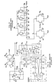
- the principal circuit blocks of the carrier detection circuit of the present invention can be implemented by conventional circuit techniques. For purposes of illustration of the operation of this invention, embodiments of the full wave rectifier with gain 10 and the sample integrator 11 will now be described.
- FIG. 5 One embodiment of a full wave rectifier with gain 50 suitable for use with this invention is shown in Fig. 5.
- a switched capacitor approach is used whereby transistors 95, 96 and 97 are operated in accordance with the timing diagrams of Figs. 6a-6c in order to charge and discharge capacitors 94 and 99.
- switched capacitors see K. Irie, et al., "A Single-Chip ADM LSI Codec", IEEE Tranactions on Acoustics, Speech, and Signal Processing, v.31, No. 1, February 1983, p. 281, at p. 283, which is hereby incorporated by reference.
- the operation of the rectifier of Fig. 5 can be understood with reference to the timing diagrams of Figs. 6a-6c.
- the switching sequence is controlled by the sign of the incoming carrier signal V in ⁇
- a comparator (not shown) provides the rectifier with gain 50 with the sign of the input signal V in ⁇
- V in' clock signals ⁇ 1 and 0 2 both go high.
- the operational amplifier 98 is thus placed in the unity gain mode, capacitor 99 is discharged, and the inherent offset voltage operational amplifier 98 is present on both the inverting input lead and the output lead of operational amplifier 98.
- FIG. 2 Another embodiment of a rectifier with gain circuit 19 suitable for use in accordance with this invention is illustrated in Fig. 2.
- the input signal V in from input lead 16 is provided to the inverting input lead of operational amplifier 23.
- the noninverting input lead of operational amplifier 23 is connected to a reference voltage obtained by the voltage drop across resistor R .
- the source of the voltage applied to resistor R a is either the negative supply V ss or the positive supply V dd depending upon which of MOS switches 20 or 21 is turned on.
- the actuation of either of MOS switches 20 or 21 is controlled by latch 24 which is driven by the clock signal supplied on line 25 and holds the information as to polarity of the input signal.
- the switching of transistors 20, 21 is selected in such a manner as to complement the instantaneous polarity of the incoming signal. For example, when V in is positive, the signal on the output lead operational amplifier 23 goes low, turning switch 20 on and switch 21 off, thus applying a negative (V ss is negative) input signal on the noninverting input lead of operational amplifier 23. Then, in order to cause the output signal provided on the output lead of operational amplifier 23 to go high, V in must become more negative. In contrast, when V in is negative, the signal on the output lead of operational amplifier 23 goes high, turning switch 20 off and switch 21 on, thus applying a positive (U DD is positive) input signal on the noninverting input lead of operational amplifier 23. Then, in order to cause the output signal provided on the output lead of operational amplifier 23 to go low, V in must become more positive. This provides a hysterysis which is necessary to suppress transistions of the comparators due to presence of noise.
- Rectification of the input signal V in occurs by the use of a switched capacitor gain stage under a controlled switching sequence as described in Figs. 6a, 6b, 6c.
- Operational amplifier 44 of Fig. 2 is analagous to operational amplifier 98 of Fig. 5.
- Switch 97 in Fig. 5 is analogous to switch 40 in Fig. 2.
- switches 28 and 29 in Fig. 2 are analagous to switches 95 and 96, respectively, in Fig. 5.
- Capacitor 94 (in Fig. 5) consists of any combination of capacitors 45, 46, 47 in Fig. 2.
- the embodiment of Fig. 2 permits any combination of capacitors 45, 46 or 47 to be used to program the closed loop gain of operational amplifier 44.
- capacitor 45 The selection of capacitor 45 is made by having signal X 4 high and signal x5 low; of capacitor 46 by having X l low and X 2 high; and of capacitor 47 by having X 6 low and X 3 high. Capacitor 45, 46, 47 serve to set the closed loop gain of operational amplifier 44 and thus the gain of stage 19.
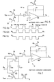
- FIG. 7 One embodiment of the sampled integrator 11 of Fig. 1 is shown in Fig. 7. This embodiment entails the use of a switched capacitor integrator, as described in the K. Irie, et al., reference cited above.
- the purpose of the sampled integrator is to integrate the output signal from rectifier 10 (Fig. 1).
- Clock phase ⁇ 5 periodically goes high in order to turn on transistor 101 and thus discharge capacitor 102.
- the ratio of the capacitance of capacitor 102 to the capacitance of capacitor 107 determines the closed loop gain of amplifier 100.
- the input voltage Vrect applied to the source of transistor 109 is provided by the output signal from the preceding full wave rectification with gain stage 10 (Fig. 1).
- Clocks ⁇ 1 and ⁇ 3 go high in order to turn on switches 103, 109 and turn off switches 104, 110 and thus charge capaci- tor C 107 to V rect (node b) minus ground (node a).
- Ther, clocks ⁇ 1 and ⁇ 3 go low to turn off transistors 103, 109 and turn on transistors 104 and 110. This causes node b to be connected to ground and node a is forced to go to virtual ground by being connected to the inverting input lead of operational amplifier 100. As a result of this, the input voltage V rect is integrated on capacitor 102 and appears on output terminal c.
- the input stage (103, 104, 109, 110) is repeatedly used in this fashion and the output signal on the integrator output lead c continues to update its old output value by adding the incremental output voltage charge provided by the operation of switches 103, 104, 109 and 110.
- the integrator is reset by clock ⁇ 5 going high, thus closing switch 101 to discharge capacitor 102.
- Switches 105 and 106 when turned on by a high clock ⁇ 6 connect capacitor 108 in parallel with capacitor 107, thus increasing the effective capacitance connected between nodes a and b. This is useful in changing the gain of the integrator.
- FIG. 3 Another embodiment of a sampled integrator 11 suitable for use in this invention is shown in Fig. 3.
- This embodiment is a switched capacitor integrator which is programmable to permit capacitors, e.g., capacitors 72 and 73, to be selected singularly or in combination as the gain setting capacitors for operational amplifier 67 and thus for integrator 11. Selection of capacitors 72, 73 is made by means of the control line 5.
- a subcircuit 9 for generation of a clock signal is shown in the lower left-hand portion of Fig. 3. If desired, such a subcircuit can be provided for each clock used in switched capacitor integrator 11, but is only shown for the purposes of illustration with respect to Clock 1.
- ⁇ 1 is shown as being generated by means of cross-coupled chains consisting first of NAND gate 50, inverter 52 and inverter gate 53, and secondly of NAND gate 51, inverter 54 and inverter 55.
- the clock 1 and clock 1 signals are supplied as control signals to MOS switches 56 and 57.
- MOS switches 56 and 57 are supplied as control signals to MOS switches 56 and 57.
- All clock signals are generated are such that the clock signals used to control each pair of switches (e.g., switches 56, 57) are nonoverlapping,
- the input voltage Vrect to the integrator 11 is supplied to the sources of transistors 61 and 62.
- switches 63, 64, 57 turn off and switches 61, 62 and 56 are turned on, thus connecting node b to V rect , and connecting node a to ground, thereby charging capaci- to r C58 to (V rect -0).
- ⁇ 1 and ⁇ 8 go high thus turning on transistors 57, 63, 64.
- node b is connected to ground and node a is connected to virtual ground, thus discharging capacitor C58 through capacitor 72, thereby integrating the input signal V rect on integrator capacitor 72.
- the integrated output voltage V int is available from node c, the output lead of opeational amplifier 67.
- ⁇ 8 goes high (transistors 63, 64 turn on) and ⁇ 1 goes low (transistor 56 turns on), thus connecting nodes a and b to ground, and discharging capacitor C58. Then, ⁇ 8 goes low (transistors 61, 62 turn on) and ⁇ 1 goes high (transistor 57 turns on), integrating the input signal V rect on integrator capacitor 72.
- This alternative sequence of steps produces an output voltage having opposite sign to that of the output voltage produced by the earlier sequence.
- a comparator 12 suitable for use with this invention is shown in Fig. 4.
- the particular embodiment shown in Fig. 4 includes a hysterysis feature.
- the input voltage V int is received from output node c of integrator 11 (Figs. 1, 3) and presented to the sources of transistors 80 and 81 which are controlled, respectively, by clocking signals ⁇ 2 and ⁇ 2 .
- the reference voltage V ref is supplied to.the sources of transistors 82 and 83 whose gates are controlled, respectively, by clocking signals ⁇ 1 and ⁇ 1 .
- the polarity of difference between V int and V ref indicates whether the input voltage V int exceeds the value of the reference voltage V ref ⁇ Thus, it is important to amplify this difference and determine this polarity, i.e., to determine when V int crosses over V ref ⁇
- This difference signal with appropriate polarity is provided on output node d after being amplified by the four amplifier stages.
- Each gain stage includes an MOS switch, a capacitor and an inverting amplifier.
- the first stage consists of MOS switch 75, capacitor 88 and amplifier 84; the second stage consists of MOS switch 76, capacitor 89 and amplifier 85; the third stage consists of MOS switch 77, capacitor 90 and amplifier 86; and the fourth stage consists of MOS switch 78, capacitor 91 and amplifier 87.
- the output difference voltage V comp supplied on output terminal d is available for input to the digital counter chain 13 of Fig. 1.
- Vref is related to the protocol defining the acceptable threshold signal.
- V ref is higher for higher threshold values and lower for lower threshold values.
- Vref is programmable on the integrated circuit chip to permit different power levels to be used to define when a carrier is present. This programmability also permits the detection of different energy levels which can be used, for example, for automatic gain control. For example, in one embodiment n different energy levels are detected by employing n different voltage references, and the result is stored in a memory. These results can then directly control the gain of a digitally programmable gain stage, with greater gain being provided for lower level input signal levels.
- hysterysis is provided in the comparator circuit of Fig. 4.
- One embodiment causes V ref to change slightly as a function of the output signal V com p on output terminal d.
- V ref Xdbm, where X is a selected value.
- the sense of the output signal is that if V int is greater than Xdbm, then a digital "1" is signified; if V int is less than Ydbm (where Y is a selected value less than X) a digital "0" is signified.
- the output remains a digital "1" for small fluctuations of the absolute value of input signal V int ⁇
- the reference voltage V ref is decreased by a small amount.
- the reverse approach can, if desired, also be used by increasing the value of Vref once a digital "0" is reached, e.g., once Ydbm is detected.
- the output signal V comp of comparator 12 is introduced to the digital counting chain 13 (Fig. 1).
- Counting chain 13 counts the time that a particular digital state, e.g. a digital "I", is present, providing that state signifies that a carrier signal of sufficient threshold amplitude is present on the input lead.
- a particular digital state e.g. a digital "I”
- determination of the threshold amplitudes it is necessary to detect a mark for a specified period of time in order for a satisfactory carrier signal to be indicated to be present.
- the mark is detected in subcircuit 14, of well known design. This mark will represent a logical "1" (i.e., carrier is received having a frequency representing a logical one).
- digital counter chain 13 also contains a delay which requires a digital "1" to be absent for at least a predefined minimum period of time in order to provide an output signal on line 17 which signifies the absence of a carrier signal.
- the output signal on line 17 will continue to indicate the presence of a carrier in order to prevent undesired termination of the transmission of data due to a very short, and inconsequential, absence of a carrier.
Landscapes
- Engineering & Computer Science (AREA)
- Computer Networks & Wireless Communication (AREA)
- Signal Processing (AREA)
- Quality & Reliability (AREA)
- Analogue/Digital Conversion (AREA)
- Burglar Alarm Systems (AREA)
- Interface Circuits In Exchanges (AREA)
- Circuits Of Receivers In General (AREA)
- Dc Digital Transmission (AREA)
Priority Applications (1)
| Application Number | Priority Date | Filing Date | Title |
|---|---|---|---|
| AT84201817T ATE47263T1 (de) | 1983-12-07 | 1984-12-06 | Traegererfassungsschaltung. |
Applications Claiming Priority (2)
| Application Number | Priority Date | Filing Date | Title |
|---|---|---|---|
| US06/559,157 US4554508A (en) | 1983-12-07 | 1983-12-07 | Carrier detection circuit |
| US559157 | 1983-12-07 |
Publications (3)
| Publication Number | Publication Date |
|---|---|
| EP0145101A2 true EP0145101A2 (de) | 1985-06-19 |
| EP0145101A3 EP0145101A3 (en) | 1986-08-20 |
| EP0145101B1 EP0145101B1 (de) | 1989-10-11 |
Family
ID=24232488
Family Applications (1)
| Application Number | Title | Priority Date | Filing Date |
|---|---|---|---|
| EP84201817A Expired EP0145101B1 (de) | 1983-12-07 | 1984-12-06 | Trägererfassungsschaltung |
Country Status (6)
| Country | Link |
|---|---|
| US (1) | US4554508A (de) |
| EP (1) | EP0145101B1 (de) |
| JP (1) | JPS60139030A (de) |
| AT (1) | ATE47263T1 (de) |
| CA (1) | CA1218425A (de) |
| DE (1) | DE3480153D1 (de) |
Cited By (3)
| Publication number | Priority date | Publication date | Assignee | Title |
|---|---|---|---|---|
| EP0231281A4 (de) * | 1985-07-18 | 1989-12-19 | Roland T Gerhart | Sicherheits- und alarmsystem. |
| WO1999017508A1 (en) * | 1997-10-01 | 1999-04-08 | Rosemount Inc. | Fsk demodulator using a super linear integrator |
| CN111034138A (zh) * | 2017-08-22 | 2020-04-17 | 德克萨斯仪器股份有限公司 | 小型且无缝的载波检测器 |
Families Citing this family (14)
| Publication number | Priority date | Publication date | Assignee | Title |
|---|---|---|---|---|
| US5638375A (en) * | 1988-11-30 | 1997-06-10 | Motorola, Inc. | AGC isolation of information in TDMA systems |
| US4945229A (en) * | 1988-12-29 | 1990-07-31 | Thomas & Betts Corporation | Fiber optic receiver and transceiver |
| US5012492A (en) * | 1989-09-29 | 1991-04-30 | Ge Fanuc Automation North America, Inc. | Apparatus and method for detecting a carrier signal |
| US5634202A (en) * | 1993-11-09 | 1997-05-27 | Motorola, Inc. | Method and apparatus for integrating a plurality of analog input signals prior to transmitting a communications signal |
| FR2724517B1 (fr) * | 1994-09-14 | 1996-12-13 | Sgs Thomson Microelectronics | Detecteur de perte de porteuse dans un modem de telecopieur |
| JP2780696B2 (ja) * | 1996-02-01 | 1998-07-30 | 日本電気株式会社 | キャリア検出装置 |
| FR2748878B1 (fr) * | 1996-05-14 | 1998-06-26 | Alcatel Telspace | Systeme de detection de la presence d'une onde porteuse d'un signal numerique et recepteur comprenant un tel systeme |
| US6539524B1 (en) * | 2000-05-10 | 2003-03-25 | Agere Systems Inc. | Method and apparatus for matching capacitance of filters having different circuit topologies |
| DE10025581A1 (de) | 2000-05-24 | 2001-12-13 | Infineon Technologies Ag | Vorrichtung und Verfahren zur Überprüfung, ob ein Signal mit einer vorbestimmten Frequenz empfangen wird |
| DE60008094T2 (de) | 2000-07-24 | 2004-07-01 | Stmicroelectronics S.R.L., Agrate Brianza | Integrator mit Gleichrichtungsfunktion und mit einem der Speisespannung entsprechenden Ausgangsspannungsbereich |
| KR100396010B1 (ko) * | 2000-08-02 | 2003-08-27 | 샤프 가부시키가이샤 | 캐리어 검출 회로 및 적외선 리모콘 수신기 |
| KR100902487B1 (ko) * | 2001-08-08 | 2009-06-10 | 엔엑스피 비 브이 | 집적 회로 및 이를 구비한 데이터 캐리어 |
| DE102005026086B3 (de) * | 2005-06-07 | 2006-09-14 | Atmel Germany Gmbh | Verfahren und Vorrichtung zum Ermitteln der Belegung eines Übertragungskanals |
| US12574126B2 (en) * | 2021-02-02 | 2026-03-10 | Northeastern University | Ultra low power wake up radio architecture |
Family Cites Families (13)
| Publication number | Priority date | Publication date | Assignee | Title |
|---|---|---|---|---|
| GB1342383A (en) * | 1970-08-03 | 1974-01-03 | Marconi Co Ltd | Signal compression and expansion systems |
| US3766479A (en) * | 1971-10-04 | 1973-10-16 | Ncr | Carrier detection circuit |
| US3746993A (en) * | 1971-12-27 | 1973-07-17 | Ncr | Carrier detection circuit |
| JPS5635342B2 (de) * | 1973-11-07 | 1981-08-17 | ||
| GB2059202B (en) * | 1979-09-14 | 1983-11-02 | Plessey Co Ltd | Digitally controlled wide range automatic gain control |
| JPS5658306A (en) * | 1979-10-18 | 1981-05-21 | Nec Corp | Automatic gain control circuit |
| FR2469837A1 (fr) * | 1979-11-07 | 1981-05-22 | Trt Telecom Radio Electr | Dispositif de detection de porteuse dans un modem muni d'un annuleur d'echo |
| DE3121444A1 (de) * | 1981-05-29 | 1982-12-16 | Siemens AG, 1000 Berlin und 8000 München | Verfahren und anordnung zum demodulieren von fsk-signalen |
| JPS5853259A (ja) * | 1981-09-25 | 1983-03-29 | Fujitsu Ltd | 搬送波検出回路 |
| JPS5856555A (ja) * | 1981-09-29 | 1983-04-04 | Fujitsu Ltd | 復調制御方式 |
| US4441082A (en) * | 1981-10-09 | 1984-04-03 | American Microsystems, Inc. | Switched capacitor automatic gain control loop |
| US4423519A (en) * | 1982-01-20 | 1983-12-27 | Sperry Corporation | Apparatus and method for detecting the onset of a frequency shift keyed signal |
| JPS58172052A (ja) * | 1982-04-02 | 1983-10-08 | Nec Corp | 信号検出器 |
-
1983
- 1983-12-07 US US06/559,157 patent/US4554508A/en not_active Expired - Lifetime
-
1984
- 1984-11-22 CA CA000468416A patent/CA1218425A/en not_active Expired
- 1984-12-06 EP EP84201817A patent/EP0145101B1/de not_active Expired
- 1984-12-06 DE DE8484201817T patent/DE3480153D1/de not_active Expired
- 1984-12-06 AT AT84201817T patent/ATE47263T1/de not_active IP Right Cessation
- 1984-12-07 JP JP59257763A patent/JPS60139030A/ja active Pending
Cited By (4)
| Publication number | Priority date | Publication date | Assignee | Title |
|---|---|---|---|---|
| EP0231281A4 (de) * | 1985-07-18 | 1989-12-19 | Roland T Gerhart | Sicherheits- und alarmsystem. |
| WO1999017508A1 (en) * | 1997-10-01 | 1999-04-08 | Rosemount Inc. | Fsk demodulator using a super linear integrator |
| CN111034138A (zh) * | 2017-08-22 | 2020-04-17 | 德克萨斯仪器股份有限公司 | 小型且无缝的载波检测器 |
| CN111034138B (zh) * | 2017-08-22 | 2023-06-06 | 德克萨斯仪器股份有限公司 | 小型且无缝的载波检测器 |
Also Published As
| Publication number | Publication date |
|---|---|
| EP0145101B1 (de) | 1989-10-11 |
| CA1218425A (en) | 1987-02-24 |
| US4554508A (en) | 1985-11-19 |
| ATE47263T1 (de) | 1989-10-15 |
| EP0145101A3 (en) | 1986-08-20 |
| DE3480153D1 (en) | 1989-11-16 |
| JPS60139030A (ja) | 1985-07-23 |
Similar Documents
| Publication | Publication Date | Title |
|---|---|---|
| US4554508A (en) | Carrier detection circuit | |
| US6480589B1 (en) | CPE alert signal detector and caller identification detector using peak detection | |
| EP0077266B1 (de) | Rückkopplungsschaltung zur automatischen Verstärkungsregelung mit schaltbaren Kondensatoren | |
| EP0508360B1 (de) | Abgetastete Bandabstandreferenzspannungsschaltung | |
| US4661802A (en) | Digital-to-analog converter | |
| US6937847B2 (en) | Integrated RF signal level detector usable for automatic power level control | |
| EP0169535A2 (de) | Analog-Digital-Wandler | |
| US3851266A (en) | Signal conditioner and bit synchronizer | |
| EP0540052A1 (de) | Störspannungsfreier Phasendetektor unter Verwendung von zwei Abtast-Halteschaltungen | |
| WO1982000390A1 (en) | Use of single reference voltage for analog to digital or digital to analog conversion of bipolar signals | |
| US4350975A (en) | Dual bandwidth autozero loop for a voice frequency CODEC | |
| US4608464A (en) | Interface circuit interconnecting a bidirectional two-wire line with unidirectional four-wire lines | |
| CA1092203A (en) | Gain ranging amplifier system | |
| CA1094174A (en) | Sampling filter-detector | |
| JPH0786513B2 (ja) | データ受信装置 | |
| US6686861B1 (en) | Slice circuit capable of accurate conversion of an analog signal to a digital signal | |
| US4291275A (en) | Frequency demodulation system | |
| JPH0215713A (ja) | アナログ・ディジタル変換回路 | |
| KR100383849B1 (ko) | 데이터 전송중 메인-동기 간섭신호를 탐지하는 방법 및 장치 | |
| US6891407B2 (en) | Analog signal level detecting apparatus | |
| US4145580A (en) | Multi-frequency signal receiver | |
| CA1234881A (en) | Carrier detection circuit | |
| US4429239A (en) | Combined phase detector and low pass filter | |
| US4730265A (en) | Split-phase matched filter using single comparator | |
| EP0145100A2 (de) | Offsetverminderung für schnelle Komparatoren mit in Serie geschalteten Eintaktverstärkerstufen |
Legal Events
| Date | Code | Title | Description |
|---|---|---|---|
| PUAI | Public reference made under article 153(3) epc to a published international application that has entered the european phase |
Free format text: ORIGINAL CODE: 0009012 |
|
| AK | Designated contracting states |
Designated state(s): AT DE FR GB IT NL SE |
|
| PUAL | Search report despatched |
Free format text: ORIGINAL CODE: 0009013 |
|
| AK | Designated contracting states |
Kind code of ref document: A3 Designated state(s): AT DE FR GB IT NL SE |
|
| 17P | Request for examination filed |
Effective date: 19861202 |
|
| 17Q | First examination report despatched |
Effective date: 19880705 |
|
| GRAA | (expected) grant |
Free format text: ORIGINAL CODE: 0009210 |
|
| AK | Designated contracting states |
Kind code of ref document: B1 Designated state(s): AT DE FR GB IT NL SE |
|
| PG25 | Lapsed in a contracting state [announced via postgrant information from national office to epo] |
Ref country code: SE Effective date: 19891011 Ref country code: NL Effective date: 19891011 Ref country code: IT Free format text: LAPSE BECAUSE OF FAILURE TO SUBMIT A TRANSLATION OF THE DESCRIPTION OR TO PAY THE FEE WITHIN THE PRESCRIBED TIME-LIMIT;WARNING: LAPSES OF ITALIAN PATENTS WITH EFFECTIVE DATE BEFORE 2007 MAY HAVE OCCURRED AT ANY TIME BEFORE 2007. THE CORRECT EFFECTIVE DATE MAY BE DIFFERENT FROM THE ONE RECORDED. Effective date: 19891011 Ref country code: AT Effective date: 19891011 |
|
| REF | Corresponds to: |
Ref document number: 47263 Country of ref document: AT Date of ref document: 19891015 Kind code of ref document: T |
|
| ET | Fr: translation filed | ||
| REF | Corresponds to: |
Ref document number: 3480153 Country of ref document: DE Date of ref document: 19891116 |
|
| NLV1 | Nl: lapsed or annulled due to failure to fulfill the requirements of art. 29p and 29m of the patents act | ||
| PLBE | No opposition filed within time limit |
Free format text: ORIGINAL CODE: 0009261 |
|
| 26N | No opposition filed | ||
| PGFP | Annual fee paid to national office [announced via postgrant information from national office to epo] |
Ref country code: SE Payment date: 19901121 Year of fee payment: 7 |
|
| ITTA | It: last paid annual fee | ||
| REG | Reference to a national code |
Ref country code: FR Ref legal event code: TP Ref country code: FR Ref legal event code: CD |
|
| REG | Reference to a national code |
Ref country code: GB Ref legal event code: IF02 |
|
| REG | Reference to a national code |
Ref country code: FR Ref legal event code: TP |
|
| REG | Reference to a national code |
Ref country code: FR Ref legal event code: TP |
|
| PGFP | Annual fee paid to national office [announced via postgrant information from national office to epo] |
Ref country code: GB Payment date: 20031203 Year of fee payment: 20 |
|
| PGFP | Annual fee paid to national office [announced via postgrant information from national office to epo] |
Ref country code: FR Payment date: 20031218 Year of fee payment: 20 |
|
| PGFP | Annual fee paid to national office [announced via postgrant information from national office to epo] |
Ref country code: DE Payment date: 20040202 Year of fee payment: 20 |
|
| PG25 | Lapsed in a contracting state [announced via postgrant information from national office to epo] |
Ref country code: GB Free format text: LAPSE BECAUSE OF EXPIRATION OF PROTECTION Effective date: 20041205 |
|
| REG | Reference to a national code |
Ref country code: GB Ref legal event code: PE20 |