EP0145533B1 - Multiplizierverfahren und -netzwerk für die Multiplikation, modulo eine Binärzahl N, zweier Binärzahlen X und Y - Google Patents
Multiplizierverfahren und -netzwerk für die Multiplikation, modulo eine Binärzahl N, zweier Binärzahlen X und Y Download PDFInfo
- Publication number
- EP0145533B1 EP0145533B1 EP19840402131 EP84402131A EP0145533B1 EP 0145533 B1 EP0145533 B1 EP 0145533B1 EP 19840402131 EP19840402131 EP 19840402131 EP 84402131 A EP84402131 A EP 84402131A EP 0145533 B1 EP0145533 B1 EP 0145533B1
- Authority
- EP
- European Patent Office
- Prior art keywords
- multiplier
- multiplier circuit
- multiplication
- circuit
- output
- Prior art date
- Legal status (The legal status is an assumption and is not a legal conclusion. Google has not performed a legal analysis and makes no representation as to the accuracy of the status listed.)
- Expired
Links
Images



Classifications
-
- G—PHYSICS
- G06—COMPUTING OR CALCULATING; COUNTING
- G06F—ELECTRIC DIGITAL DATA PROCESSING
- G06F7/00—Methods or arrangements for processing data by operating upon the order or content of the data handled
- G06F7/38—Methods or arrangements for performing computations using exclusively denominational number representation, e.g. using binary, ternary, decimal representation
- G06F7/48—Methods or arrangements for performing computations using exclusively denominational number representation, e.g. using binary, ternary, decimal representation using non-contact-making devices, e.g. tube, solid state device; using unspecified devices
- G06F7/52—Multiplying; Dividing
- G06F7/523—Multiplying only
- G06F7/527—Multiplying only in serial-parallel fashion, i.e. one operand being entered serially and the other in parallel
- G06F7/5277—Multiplying only in serial-parallel fashion, i.e. one operand being entered serially and the other in parallel with column wise addition of partial products
-
- G—PHYSICS
- G06—COMPUTING OR CALCULATING; COUNTING
- G06F—ELECTRIC DIGITAL DATA PROCESSING
- G06F2207/00—Indexing scheme relating to methods or arrangements for processing data by operating upon the order or content of the data handled
- G06F2207/38—Indexing scheme relating to groups G06F7/38 - G06F7/575
- G06F2207/3804—Details
- G06F2207/386—Special constructional features
- G06F2207/3884—Pipelining
- G06F2207/3892—Systolic array
-
- G—PHYSICS
- G06—COMPUTING OR CALCULATING; COUNTING
- G06F—ELECTRIC DIGITAL DATA PROCESSING
- G06F7/00—Methods or arrangements for processing data by operating upon the order or content of the data handled
- G06F7/38—Methods or arrangements for performing computations using exclusively denominational number representation, e.g. using binary, ternary, decimal representation
- G06F7/48—Methods or arrangements for performing computations using exclusively denominational number representation, e.g. using binary, ternary, decimal representation using non-contact-making devices, e.g. tube, solid state device; using unspecified devices
- G06F7/499—Denomination or exception handling, e.g. rounding or overflow
- G06F7/49931—Modulo N reduction of final result
Definitions
- the invention relates to a method and a multiplier network for multiplying, modulo a binary number N, of two binary numbers X and Y represented by digital signals.
- the calculations of the exponential functions are most often carried out, either using programmed logical structures, or by the intermediary of integrated multiplier circuits, working for example, on numbers of twice 16 bits in parallel to give results on a length of 32 bits.
- the disadvantage of these devices is that, for very large binary numbers, the calculation of an exponential function takes a considerable time which can vary, for example, when the binary numbers have lengths of 128 bits, from two seconds to one minute depending on the structure of the operator used.
- a time of two seconds can be obtained by using a logic wired around a multiplier circuit operating on numbers of twice 16 bit and controlled by a 16 bit microprocessor.
- this time can be increased to ten seconds if in the previous embodiment the 16-bit microprocessor is replaced by an 8-bit microprocessor.
- a largely prohibitive time, of one minute can be obtained by simply using an 8-bit microprocessor of the type for example 6802 sold by the company MOTOROLA.
- the invention aims to overcome the aforementioned drawbacks.
- the subject of the invention is a method of multiplying, modulo a binary number N, of two binary numbers X, Y represented by digital signals respectively multiplier and multiplicand characterized in that it consists in carrying out a first multiplication of the multiplier signal by the multiplicand signal using a first multiplier circuit, performing a second multiplication of the result obtained at the output of the first multiplier circuit by a digital signal representing the inverse of the number N using a second multiplier circuit, to take the integer part of the result obtained at the output of the second multiplier circuit, to effect a third multiplication of the integer part obtained by a digital signal representing the number N using a third multiplier circuit, and to subtract the result obtained at the output of the third multiplier circuit from the result obtained at the output of the first multiplier circuit ator, to obtain a digital signal R corresponding to the product modulo the number N, of the multiplier number X by the multiplicand number Y.
- the invention also relates to a multiplier circuit and a multiplier network for the implementation of the aforementioned modulo N multiplication method.
- the method according to the invention follows from the preceding remarks; it consists, in a first step, in calculating the number A by performing the product of the two numbers X and Y, in performing in a second step the product of the number A obtained in the first step by the number I N , the result obtained being equal to the number Q, to be carried out in a third step, the product of the number N by the number Q and to subtract in the fourth step the product NQ of the number A, to obtain the number R.
- the only difficulty which can be encountered in carrying out the steps of the method can consist in determining the inverse of the number N to calculate the number I N. This difficulty seems to be able to be overcome in most practical cases, ca the number N is generally fixed by the operation modulo N which one seeks to execute and its inverse can easily be obtained. If the number I N is calculated by default we will of course have an uncertainty on the value of the number Q found. The fact that in this case the number I N is equal to involves expressions
- the numbers A and N are respectively composed of 2p and p binary elements the precision on the number I N appears sufficient if the number s is less than or equal to 2- 2 P.
- the number Q ' is either equal the number Q is equal to the number Q - 1.
- the result R is either good or increased by the number N.
- the process which has just been described can easily be extended to obtaining the product of two binary numbers X, Y, the result being obtained modulo a binary number N.
- the result of the multiplication can be obtained by using three times the same multiplicative structure, a first time to calculate the product X x Y, a second time to calculate the product A x I N and a third time to calculate the product Q x N.
- the numbers X, Y and N each have p bits, it is possible to give them the following binary representations
- the number B obtained is then equal to the product of the numbers A 'and the N of expressions (12) and (13) either
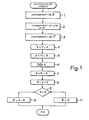
- step 1 shows, in the form of a flowchart, the progress of the various stages of execution of the method according to the invention.
- the numbers X, k, N and Y represented using digital signals are loaded into registers of the microprogrammed structure or of the wired logic and a first multiplication of the number X by the number Y is performed in step 4 to give a number A.
- step 5 a second multiplication of the number A by the number I N is performed to give a number B from which the integer part Q is extracted in step 6.
- L step 7 consists in making the product of the number Q by the number N to obtain the number U which is subtracted from the number A in step 8 to provide the number R.
- the number R is compared to the number N .
- step 10 consists in subtracting the number N from the number R obtained to obtain a number R 'which is taken into account as the remainder of the modulo N operation and if in step 9 the number R is smaller than the number N, the remainder R 'taken into account in step 11 will be equal to the remainder R obtained in step 8.
- a multiplier network for multiplying modulo a binary number N of two binary numbers X and Y making it possible to execute the steps of the aforementioned method is represented in FIG. 2.
- the logical structure of the network represented in FIG. 2 comprises a set of registers 12 , 13, 14 and 15 whose containers are loaded at the initialization of the process respectively by the binary numbers X, Y, and the number N.
- the register 12 is connected to a first input of a multiplier circuit 16 through a shift register 17, the second input of the multiplier circuit 16 being connected to the output of the register 13.
- the multiplier circuit 16 operates the multiplication of the binary numbers X and Y, and applies the number A, obtained as a result, to a first input of a second multiplier circuit 18 through a shift register 19.
- the second input of the multiplier circuit 18 is connected to the output of the register 14.
- the multiplier circuit 18 operates the multiplication of the number A calculated by the multiplier 16 and transferred into register 19 by the number 1 N contained in the register 14, the result obtained corresponds to the number B.
- the integer part Q of the number B is extracted by a register 20 and is transferred to a shift register 21.
- a multiplier circuit 22 has a first input connected to the output of register 21 and a second input connected to the output of register 15.
- the multiplier circuit 22 performs the multiplication of the numbers Q and N contained in registers 21 and 15 respectively, and applies the result of the multiplication to a first input of a subtractor 24.
- the second input of the subtractor 24 is connected to a serial output of the register 19 through a delay line 23.
- the subtractor 24 makes it possible to subtract the number A, contained in the register 19, from the number U obtained at the output of the multiplier 22 and applies the result obtained to the entry of a register 25. At the end of the calculation operation, the number R sought appears contained in the register 25. It is then possible by means of external tests, not shown, of coming to check the magnitude of the number R with respect to that of the number N, to make the decisions of steps 9, 10 and 11 of the method according to the invention described above by means of FIG. 1.
- the multiplier circuits 16, 18 and 22 will be produced using series systolic structures according to the invention, preferably with parallel systolic structures whose complexity, to perform operations on large numbers , makes the realization of multiplier circuits practically impossible.
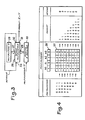
- the multiplier circuit represented in FIG. 3 comprises, a multiplication and addition network 26 coupled, by a first input 27 to a multiplicand register 28 and by a second input 29 to a shift multiplier register 30.
- the multiplication and addition network 26 also has two outputs 31 and 32, the output 31 providing the result of the multiplication of the multiplier by the multiplicand and the output 32 providing the different retentions as the multiplier circulates inside the shift register 30.
- the output 32 is looped back to a third input 33 of the multiplication network and d addition 26 to propagate the reserve obtained at each shift of the multiplier in the shift register 30.
- the table of FIG. 4 represents an operation of multiplication of two binary numbers A and B each having a length of 4 bits, the binary number A having the binary value 0101 and the binary number B having the binary value 0111, the binary values of numbers A and B corresponding respectively to decimal numbers 5 and 7.
- the binary number A corresponds to the multiplicand and is represented loaded in the register 28.
- the binary word B corresponds to the multiplier and is represented circulating in the shift register 30.
- the products obtained at each shift of the multiplier in the register 30 are represented in the product column and the corresponding deductions are represented in the retained column.
- the product obtained has the binary value 00100011 corresponding to the number 35 in base 10.
- registers 28 and 30 must include 128 rockers.
- the production of a serial systolic multiplier circuit operating according to the principle described using the table in FIG. 4 can be carried out simply using a wired circuit, composed of AND gates with two inputs and a set of exclusive OR gates, operating according to an algorithm where each bit of the multiplicand is multiplied, using an AND gate, with the corresponding bit of the same rank in the multiplier register and where the results of the elementary multiplications obtained at the output of each of the AND gates are added using exclusive OR gates.
- An exemplary embodiment of a series systolic multiplier circuit according to the invention operating according to this principle is described using the embodiment diagram in FIG. 5.
- the multiplier circuit represented in FIG. 5 comprises a set of logic AND gates with two inputs denoted respectively from 34 to 37, they receive respectively on a first input the bits a o , a 1 , a 2 , a 3 of the multiplicand and on a second input bits b o to b 3 of the multiplier.
- Each of the outputs of the gates 34 to 37 is connected respectively to an input of an exclusive OR gate 38 to 41.
- a set of exclusive OR gates 42 is provided for possibly adding a previous result S IN to possibly four deductions introduced from input C IN 0 and C IN 1 of a carry-over decoder 43.
- the outputs of AND gates 34 to 37 as well as the outputs of the carry-over decoder 43 are connected respectively to inputs of a carry-over encoder 44 which delivers on its outputs two holding signals C OUT o and C OUT ,.
- the signals C OUT o and C OUT are optionally applied to the inputs of rockers not shown external to the circuit of FIG. 5, to memorize the deductions obtained during calculation and apply the memorized deductions to the inputs C IN o and C IN 1 of the carry decoder 43.
- FIG. 6 An alternative embodiment of the four-bit multiplier circuit according to the invention is shown in Figure 6.
- the multiplier circuit is constituted by a PROM memory 45 comprising addressing inputs A o to A 10 and four data outputs Q 0 to Q 3 .
- the four-bit multiplicand a o to a 3 is applied to the address inputs A o to A 3 and the bits b o to b 3 of the multiplier are applied respectively to the address inputs A 4 to A 7 .
- the previous result, if any, is applied to the addressing input A 8 .
- the addressing inputs Ag and A 10 are used to take account of any deductions CINo and C IN, obtained during the calculation of the previous result.
- the result of the multiplication is read at each addressing on the output Q o and the deductions C OUT 0 and C OUT, which appear during calculation appear on the outputs Q 2 and Q 3 of the PROM 45 memory.
- the holding bits C OUT 0 and C OUT, appearing at the outputs Q 2 and Q 3 of the PROM memory 45 can be memorized by rockers not shown outside to be transmitted to the addressing inputs Ag and A, o , so as to take account of the deductions obtained during a calculation for the following calculation.
- the content of the PROM memory 45 is composed of a multiplication table corresponding to the 4-bit multiplication operation with propagation of two holdbacks, the programming of this PROM memory may be carried out using a simulator, not shown , and a program for simulating the multiplication operation to be performed on four bits, a flow diagram of which is shown in FIG. 7.
- the programming operation consists in entering in step 46 a table of results in the form of bytes.
- the initialization of the program consists in carrying out in steps 47 to 49 an initialization to the zero value of the parameters S IN, A and B of the program.
- the values S IN, B and A are loaded respectively into registers M 1 , M 2 and M 3 of the simulator.
- step 54 The content of a counter of the results of the simulator is increased by one unit in step 54 each time the value S IN is placed in the logical state 1 which causes a new calculation in step 55 of the state of the output S OUT, as well as a new calculation in step 56 of the output C OUT according to the state of the counter.
- step 58 the results S OUT and C OUT are stored in the form of a byte at the location of the PROM memory corresponding to the addresses indicated by the registers M 1 , M 2 and M 3 loaded in step 50
- the byte obtained in step 57 is also stored in a register of the simulator and increased by one unit in step 58.
- step 59 the content of address register M 3 is increased by one unit.
- step 60 a test is performed on the content of the register M 3 , if this content is less than the binary number 1111 the program returns to step 50 on the other hand, if the content M 3 is greater than the binary number 1111 on program continues with step 61 which consists in increasing the content of the address register M 2 by one .
- step 62 a test is carried out on the content of the address register M 2 and if this content is less than the binary number 1111 the program returns to step 49 to perform steps 39 to 62 again.
- step 63 which consists in increasing by one unit the content of the address register M l .
- step 64 a test is carried out on the content of the address register M l . As long as the content of the register M 1 is less than the binary number 111, the program runs in the loop formed by steps 48 to 64, to stop when the binary number contained in the register M 1 reaches the value 111.
- a multiplier network of two binary numbers, each composed of 128 bits, using one or the other of the systolic multiplier circuits represented in FIGS. 5 and 6 is now described with the aid of the diagram represented in FIG. the organization of the multiplicative structure represented in FIG. 3 includes a set of four-bit multiplier circuits of the type previously described in FIGS. 5 and 6, these circuits being 32 in number and numbered 66 to 97 respectively.
- the circuits 66 to 97 are connected in cascade, the input S IN of the first circuit is connected to ground and each output S OUT of a circuit is connected to the output S IN of the circuit which follows it directly.
- the outputs C OUT of each of the circuits are looped back to the corresponding input C IN by means of rockers denoted respectively from 98 to 129.
- the number A composed of 128 bits, is applied by a data bus 130 to the parallel inputs of registers with 8 rockers denoted from 131 to 146. Each group of four consecutive bits contained in a register is directed to the corresponding input of the multiplier circuits 66 to 97.
- the multiplier network of FIG. 8 also includes a set of registers with eight rockers mounted in series denoted respectively from 147 to 162, each section of four bits of a register being applied to a corresponding input of the multiplier circuits 66 to 97. Each bit of the multiplier number is entered successively, at input 163 of the register to shift formed by registers 147 to 162, at the rate of the clock of the clock signal H applied to each of the clock inputs of registers 147 to 162.
- serial systolic multiplier circuit which can work on 128, 192 or 256 bits.
- This integrated circuit produced would make it possible to develop a modulo N multiplication operator of reduced size and high operating speed. In fact, the operator could use the specific integrated circuit 3 times to satisfy the multiplicative steps of the previously described process.
Landscapes
- Physics & Mathematics (AREA)
- General Physics & Mathematics (AREA)
- Engineering & Computer Science (AREA)
- Computational Mathematics (AREA)
- Mathematical Analysis (AREA)
- Mathematical Optimization (AREA)
- Pure & Applied Mathematics (AREA)
- Theoretical Computer Science (AREA)
- Computing Systems (AREA)
- General Engineering & Computer Science (AREA)
- Complex Calculations (AREA)
Claims (11)
Applications Claiming Priority (2)
| Application Number | Priority Date | Filing Date | Title |
|---|---|---|---|
| FR8317315A FR2554257B1 (fr) | 1983-10-28 | 1983-10-28 | Procede et reseau multiplicateur pour la multiplication, modulo un nombre binaire n, de deux nombres binaires x et y |
| FR8317315 | 1983-10-28 |
Publications (2)
| Publication Number | Publication Date |
|---|---|
| EP0145533A1 EP0145533A1 (de) | 1985-06-19 |
| EP0145533B1 true EP0145533B1 (de) | 1988-03-16 |
Family
ID=9293660
Family Applications (1)
| Application Number | Title | Priority Date | Filing Date |
|---|---|---|---|
| EP19840402131 Expired EP0145533B1 (de) | 1983-10-28 | 1984-10-23 | Multiplizierverfahren und -netzwerk für die Multiplikation, modulo eine Binärzahl N, zweier Binärzahlen X und Y |
Country Status (3)
| Country | Link |
|---|---|
| EP (1) | EP0145533B1 (de) |
| DE (1) | DE3469960D1 (de) |
| FR (1) | FR2554257B1 (de) |
Families Citing this family (2)
| Publication number | Priority date | Publication date | Assignee | Title |
|---|---|---|---|---|
| FR2724741B1 (fr) * | 1994-09-21 | 1996-12-20 | Sgs Thomson Microelectronics | Circuit electronique de calcul modulaire dans un corps fini |
| US6167421A (en) * | 1998-04-09 | 2000-12-26 | Teranex, Inc. | Methods and apparatus for performing fast multiplication operations in bit-serial processors |
Family Cites Families (4)
| Publication number | Priority date | Publication date | Assignee | Title |
|---|---|---|---|---|
| US3302008A (en) * | 1964-01-16 | 1967-01-31 | Exxon Production Research Co | Multiplication device |
| US3582634A (en) * | 1968-10-15 | 1971-06-01 | Stromberg Carlson Corp | Electrical circuit for multiplying serial binary numbers by a parallel number |
| US4281391A (en) * | 1979-01-15 | 1981-07-28 | Leland Stanford Junior University | Number theoretic processor |
| GB2067799A (en) * | 1980-01-12 | 1981-07-30 | Plessey Co Ltd | Improvements in or Relating to Digital Filters |
-
1983
- 1983-10-28 FR FR8317315A patent/FR2554257B1/fr not_active Expired
-
1984
- 1984-10-23 DE DE8484402131T patent/DE3469960D1/de not_active Expired
- 1984-10-23 EP EP19840402131 patent/EP0145533B1/de not_active Expired
Also Published As
| Publication number | Publication date |
|---|---|
| FR2554257A1 (fr) | 1985-05-03 |
| DE3469960D1 (en) | 1988-04-21 |
| FR2554257B1 (fr) | 1985-12-27 |
| EP0145533A1 (de) | 1985-06-19 |
Similar Documents
| Publication | Publication Date | Title |
|---|---|---|
| EP0712072B1 (de) | Verfahren zur Ausführung von modularen Reduktion nach der Montgomery-Methode | |
| EP0712071B1 (de) | Verfahren zur Verwendung der modularen Multiplikation nach der Montgomery-Methode | |
| EP1368747B1 (de) | Verfahren und vorrichtung zur verkürzung der rechenzeit eines produktes, einer multiplikation und einer potenzierung nach der montgomery-methode | |
| EP0485921B1 (de) | Vorrichtung für die Verarbeitung des Viterbi-Algorithmus mit einem Prozessor und einer spezialisierten Einheit | |
| EP0275765B1 (de) | Integrierter Schaltkreis für Digitalsignalverarbeitung | |
| EP0204612B1 (de) | Verfahren zur Datenübertragung mit Möglichkeit zur Korrektur von Fehlerpaketen und Kodierungs- und Dekodierungsanordnung zur Durchführung dieses Verfahrens | |
| EP0145533B1 (de) | Multiplizierverfahren und -netzwerk für die Multiplikation, modulo eine Binärzahl N, zweier Binärzahlen X und Y | |
| EP0712070A1 (de) | Verfahren zum Erzeugen eines Fehlerkorrekturparameters in Verbindung mit der Verwendung von modularen Operationen nach der Montgomery-Methode | |
| EP0793165B1 (de) | Koprozessor für moduläre Arithmetik mit einer schnellen Ausführung von nicht-modulären Operationen | |
| CA2051559C (fr) | Generateur d'adresses pour la memoire de donnees d'un processeur | |
| EP0215497B1 (de) | Autokorrelationseinrichtung | |
| EP0778518B1 (de) | Verfahren zum Erzeugen eines Parameters J0 bezüglich der Verwendung von modularen Operationen nach der Montgomery-Methode | |
| FR2796736A1 (fr) | Procede pour effectuer une multiplication avec accumulation dans un corps de galois | |
| EP0927928B1 (de) | Verbessertes Verfahren zum Erzeugen eines Parameters J0 bezüglich der Verwendung von modularen Operationen nach der Montgomery-Methode | |
| FR2570853A1 (fr) | Dispositif de traitement en temps reel de signal numerique par convolution | |
| CA2359198C (fr) | Unite de calcul pour l'execution d'un protocole cryptographique | |
| EP0122843B1 (de) | Modularer Integrator | |
| EP0209446A1 (de) | Multiplizierer für die Multiplikation von zwei komplexen Nummern | |
| EP0125156B1 (de) | Kaskadierter Multiplizierer mit einer Anordnung von elementären Operatoren | |
| FR2811168A1 (fr) | Procede de conversion de la representation binaire d'un nombre dans une representation binaire signee | |
| FR2641097A1 (de) | ||
| FR2666861A1 (fr) | Generateur d'adresses pour la memoire de donnees d'un processeur. | |
| FR2738365A1 (fr) | Procede et circuits pour la multiplication modulo un nombre binaire n de deux nombres binaires et leurs utilisations aux calculs d'exponentiations | |
| FR2602073A1 (fr) | Circuit de traitement numerique de signal realisant une transformation cosinus. | |
| WO2003093973A1 (fr) | Multiplication au sens de montgomery |
Legal Events
| Date | Code | Title | Description |
|---|---|---|---|
| PUAI | Public reference made under article 153(3) epc to a published international application that has entered the european phase |
Free format text: ORIGINAL CODE: 0009012 |
|
| AK | Designated contracting states |
Designated state(s): CH DE GB LI |
|
| 17P | Request for examination filed |
Effective date: 19851014 |
|
| 17Q | First examination report despatched |
Effective date: 19861125 |
|
| GRAA | (expected) grant |
Free format text: ORIGINAL CODE: 0009210 |
|
| AK | Designated contracting states |
Kind code of ref document: B1 Designated state(s): CH DE GB LI |
|
| REF | Corresponds to: |
Ref document number: 3469960 Country of ref document: DE Date of ref document: 19880421 |
|
| GBT | Gb: translation of ep patent filed (gb section 77(6)(a)/1977) | ||
| PLBE | No opposition filed within time limit |
Free format text: ORIGINAL CODE: 0009261 |
|
| STAA | Information on the status of an ep patent application or granted ep patent |
Free format text: STATUS: NO OPPOSITION FILED WITHIN TIME LIMIT |
|
| 26N | No opposition filed | ||
| PGFP | Annual fee paid to national office [announced via postgrant information from national office to epo] |
Ref country code: CH Payment date: 19920910 Year of fee payment: 9 |
|
| PGFP | Annual fee paid to national office [announced via postgrant information from national office to epo] |
Ref country code: DE Payment date: 19920917 Year of fee payment: 9 |
|
| PGFP | Annual fee paid to national office [announced via postgrant information from national office to epo] |
Ref country code: GB Payment date: 19920918 Year of fee payment: 9 |
|
| PG25 | Lapsed in a contracting state [announced via postgrant information from national office to epo] |
Ref country code: GB Effective date: 19931023 |
|
| PG25 | Lapsed in a contracting state [announced via postgrant information from national office to epo] |
Ref country code: LI Effective date: 19931031 Ref country code: CH Effective date: 19931031 |
|
| GBPC | Gb: european patent ceased through non-payment of renewal fee |
Effective date: 19931023 |
|
| REG | Reference to a national code |
Ref country code: CH Ref legal event code: PL |
|
| PG25 | Lapsed in a contracting state [announced via postgrant information from national office to epo] |
Ref country code: DE Effective date: 19940701 |